

Page 1
AN-624
APPLICATION NOTE
One Technology Way • P.O. Box 9106 • Norwood, MA 02062-9106 • Tel: 781/329-4700 • Fax: 781/326-8703 • www.analog.com
Calibration of a 3-Phase Energy Meter Board on the ADE7754
By Etienne Moulin
INTRODUCTION
A 3-phase energy meter can interface with different
services like 3-phase 4-wire, 3-phase 3-wire, and
3-phase 4-wire with 2½ elements. It can also provide
active, reactive, and apparent energy cal c ulat ions as we ll
as power quality measurements, voltage rms, and current rms.
This application note describes the different steps to
calibrate a 3 -phase 4-wire, 3 - element energy meter
based on the ADE7754. It describes the sof tware used
with the ADE7754 evaluation board to perform the calibration.
The ADE7754 is comprised of six ADCs, a reference circuit, and all the signal processing necessary for the
calculation of active energy, apparent energy, and rms
value of the analog inputs. Circuitry is provided to null
out various system errors including gain, phase, and
offset errors. All registers of the ADE7754 are avail able through a 4-wire serial interface (SPI
to the ADE7754 data sheet for a detailed description
and the operation of the SPI interface.
3-PHASE ENERGY SERVICES
This section presents the different 3-phase services
as well as the different meter architectures available in
the fi eld. Each of these solutions uses a different formula
to calculate energy. The terms and descriptions of the
services are taken from the US ANSI C12.1 standard.
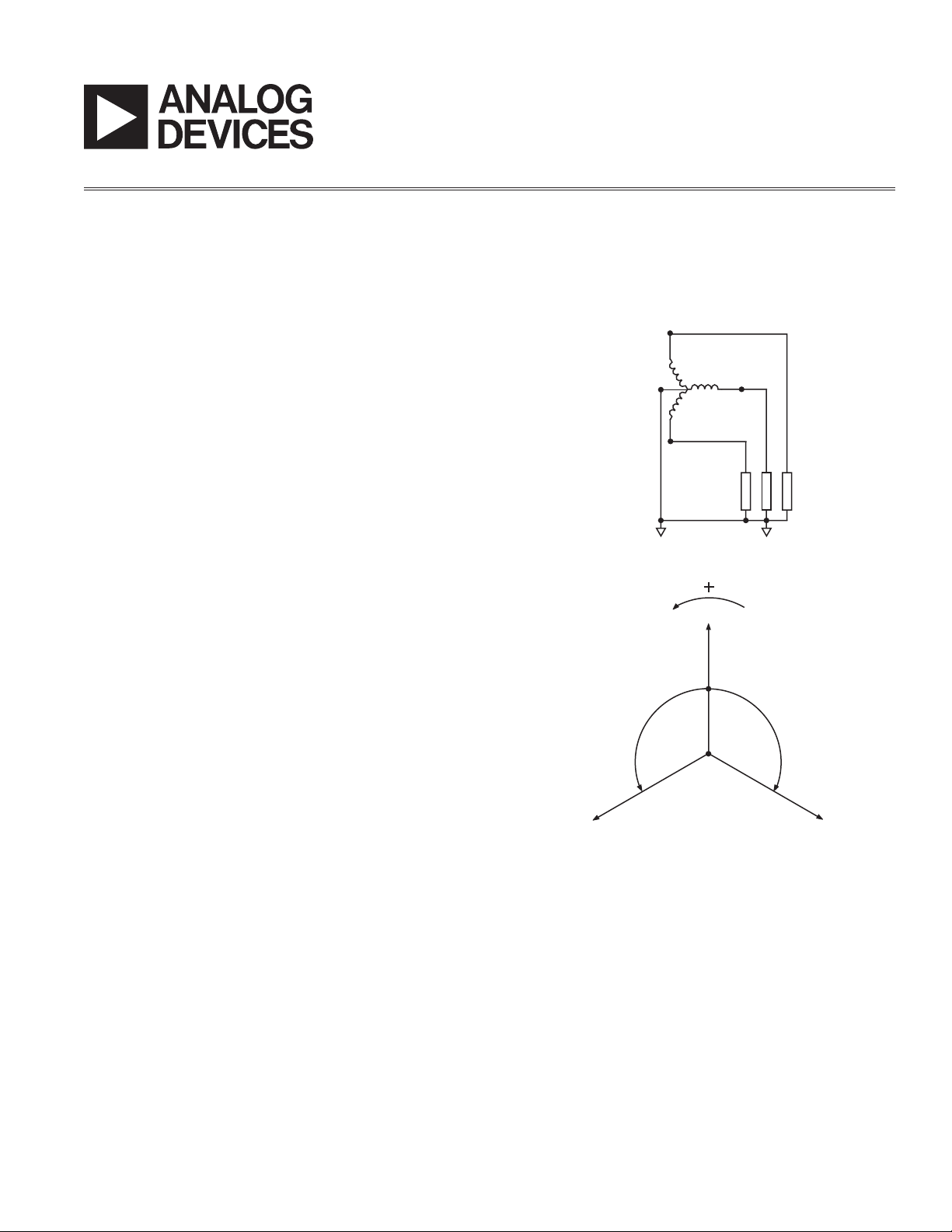
3-Phase 4-Wire Wye Service
This service is comprised of three phases and one neutral conductor, as described in Figure 1. Each voltage
phase is referred to the neutral and has ±120° phase
difference with the other phases (see Figure 2). The
energy measurement is done with three current sensors
and two or three voltage sensors. A meter with two
voltage sensors is generally called a 2½ -element or
2-stator 4-wire wye meter. A meter with three voltage
sensors is generally called a 3-element or 3-stator
4-wire wye meter.
®
). Please refer
PHASE A
SOURCE
Figure 1. 3-Phase 4-Wire Wye Service
PHASE B
Figure 2. 3-Phase 4-Wire Wye Phasor Diagram
3-Stator 4-Wire Wye Meter
This 3-phase meter is comprised of three voltage sen sors and three current sensors. The common point of
the voltage sensors should be connected to the neutral
conductor. The energy measurements are done based
on the measurement of the six entities involved in the
system. This method is accurate for all conditions of load
(balanced and unbalanced), power factor, or voltage.
Active Power = V I V I V I
PHASE B
PHASE C
LOAD
PHASE A
–120ⴗ+120ⴗ
NEUTRAL
PHASE C
×+ ×+ ×
AA BB CCφφ φφ φφ
REV. 0
Page 2
AN-624
2-Stator 4-Wire Wye Meter
This 3-phase meter is comprised of two voltage sensors and three current sensors. The common point of
the voltage sensors should be connected to the neutral
conductor. According to Blondel’s Theorem, if the voltages between each line and the neutral are balanced
within acceptable limits, the accuracy is generally considered satisfactory. The energy measurements are
done by combining the fi ve entities (two voltages and
three currents) of the system.
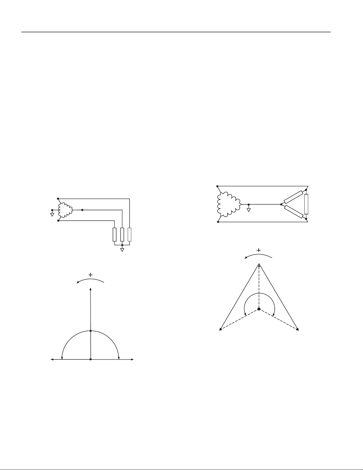
3-Phase 4-Wire Delta Service
This service is comprised of three phases and one
neutral conductor (see Figure 3). The neutral conductor
is formed by a tap to the midpoint of one of the phase
windings (see Figure 4). The energy measurement is
done with three current sensors and two or three voltage sensors. A meter with two voltage sensors is
generally called a 2½-element or 2-stator 4-wire delta
meter. A meter with three voltage sensors is generally
called a 3- element or 3 - stator 4 -wire delta meter.
PHASE A
SOURCE
PHASE C
2-Stator 4-Wire Delta Meter
This 3-phase meter is comprised of two voltage sensors
and three current sensors. The common point of the
voltage sensors should be connected to the neutral conductor. If the neutral is a true midtap (voltages used to
defi ne the neutral are equal within acceptable limits),
then only two voltage sensors need be used (2-stator).
The energy measurements are done by combining the
fi ve entities (two voltages and three currents) of the
system.
3-Phase 3-Wire Delta Service
This service is comprised of three phase conductors
(see Figure 5 and 6). The energy measurements are done
with three current sensors and two or three voltage
sensors. A meter with two voltage sensors is generally
called a 2½-element or 2-stator 4-wire delta meter. A
meter with three voltage sensors is generally called
a 3-element or 3-stator 4-wire delta meter.
PHASE A
SOURCE
PHASE C
LOAD
PHASE B
LOAD
Figure 3. 3-Phase 4-Wire Delta Service
PHASE C
–90ⴗ+90ⴗ
PHASE A
NEUTRAL
PHASE B
Figure 4. 3-Phase 4-Wire Delta Phasor Diagram
3-Stator 4-Wire Delta Meter
This 3-phase meter is comprised of three voltage sen sors and three current sensors. The common point of
the voltage sensors should be connected to the neutral
conductor. The energy measurements are done based
on the measurements of the six entities involved in the
system. This method is accurate for all conditions of load
(balanced and unbalanced), power factor, or voltage.
PHASE B
Figure 5. 3-Phase 3-Wire Delta Service
PHASE A
PHASE B – PHASE A PHASE C – PHASE A
+120ⴗ
–120ⴗ
PHASE CPHASE B
Figure 6. 3-Phase 3-Wire Delta Phasor Diagram
2-Stator 3-Wire Delta Meter
This 3-phase meter is comprised of two voltage sensors
and two current sensors. The common point of the
voltage sensors should be connected to one phase
conductor. The current sensors are connected to the
other two phase conductors.
–2–
REV. 0
Page 3

AN-624
CONFIGURATION OF ADE7754 FOR 3-PHASE ENERGY METERING
The ADE7754 provides several registers to confi gure
the part depending on the meter connections and the
desired results. Some registers are specifi c to the meter
connections, but others are more generic and their
values can be defi ned early in the design.
The OPMODE and GAIN registers defi ne the general
confi guration of the ADE7754.
OPMODE (Address 0x0A)
Usually, the OPMODE register can be set to 0x00. With
this value, the high-pass fi lters and low-pass fi lters are
enabled and the pulse output proportional to active
power, CF, is activated. The part can be reset to its
default confi guration by setting Bit 6 of this register
to Logic 1. The default value of the OPMODE register
after reset is 0x04. In this state, the CF pulse output is
disabled.
GAIN (Address 0x18)
This register defi nes the PGA gain setting of both current
and voltage channels, the mode of accumulation of the
active powers (arithmetic sum or sum of the absolute
values), and the application of a no -load threshold on
the individual active powers.
The MMODE and WAVMODE registers confi gure the
measurements processed by the ADE7754.
MMODE (Address 0x0B)
This register defi nes the phase input on which the period
measurement and the peak detection are made. It also
defi nes the phases used for counting the number of
zero crossings in the line accumulation mo des. Th is re g ister can be set at a default value at initialization and
changed during the meter operation.
WAVMODE (Address 0x0C)
This register defi nes the speed and the analog input
used for waveform sampling. The value of this register
can be defi ned at initialization and changed during the
meter operation to access the different ADC outputs.
This register also selects the accumulation of the reactive energy in the LAENERGY register if needed.
Interrupt Mask (Address 0x0F)
This register defi nes which event will drive the interrupt
request pin (IRQ) low. The detected events are:
• Active energy register half full
• Low voltage on any of the three voltage inputs (SAG)
• Missing zero-crossing on any of the three voltage
inputs (ZXTOUT)
• Rising zero-crossing edge on any of the three voltage inputs (ZX)
• End of accumulation of energy over the LINCYC line
cycles (LENERGY)
• High voltage on a selected voltage or current input
(PKV and PKI)
• Sample available in the waveform sampling register (WFSM)
• Apparent energy register half full
The selection of the events for interruption depends on
the functionality needed in the meter. It is recommended
to select the interrupts for half-full energy (active and
apparent) in order to avoid any information loss due to
the overfl ow of these registers. The other interrupts
should be selected depending on the need of the design.
The confi guration and operation of the SAG, ZXTOUT,
VPEAK, and IPEAK interrupts are detailed in the ADE7754
data sheet.
REV. 0
–3–
Page 4
AN-624
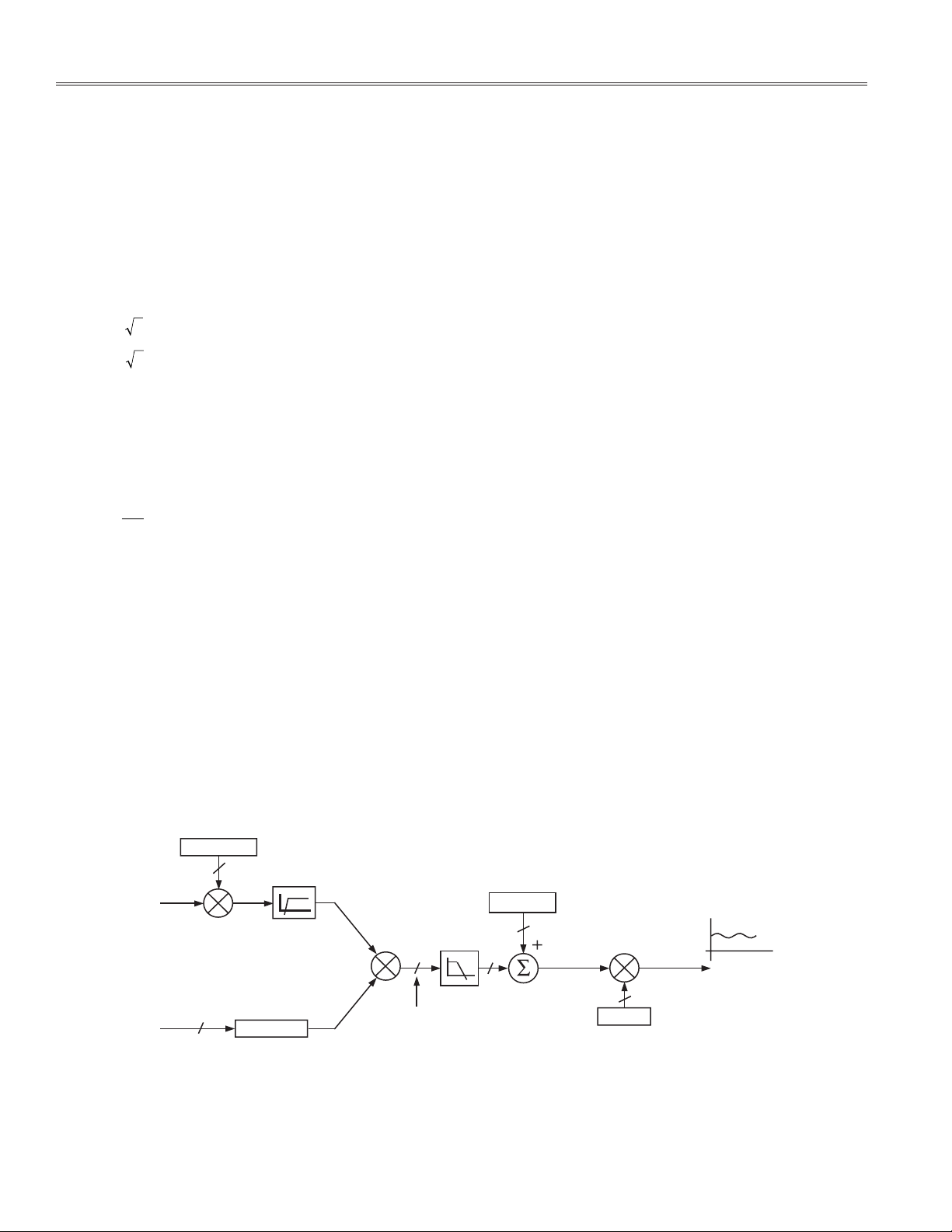
ACTIVE POWER-ENERGY MEASUREMENTS
Theory of Operation
Electrical power is defi ned as the rate of energy fl ow
from source to load. It is given by the product of the
voltage and the current inputs. The resulting signal is
called the instantaneous power signal and is equal to
the rate of active energy fl ow at every instant of time.
The unit of power is the watt or joules /sec. Equation 3
gives an expression for the instantaneous power signal
in an ac system.
v(t) V t= 2 sin( )
i(t) I ( t)= 2 sin
ω
(1)
ω
(2)
where V = rms voltage, I = rms current.
pt v t it
() () ()
=×
pt VI–VIcos t
() ( )
= 2ω
(3)
The average power over an integral number n of line
cycles is given by Equation 4.
nT
1
P
==
nT
pt dt VI
()
∫
0
(4)
where T is the line cycle period.
P is referred to as the active or real power. Note that the
active power is equal to the dc component of the instantaneous power signal p(t) in Equation 3, i.e., VI. This
is the relationship used to calculate active power in the
ADE7754 for each phase. Figure 7 shows the active
power signal processing implemented in the ADE7754
for each phase.
Due to individual sensor characteristics, the active
power calculation needs to be calibrated to correct for
gain, phase, and offset errors for each phase independently (phase balancing).
Active Energy Accumulation
Besides the pulse output, which is used for calibration
verifi cation (see the Active Power Pulse Output section),
a solid state energy meter requires some form of display. This display should show the amount of energy
consumed in kWh (kilowatt hours). One convenient and
simple way to interface the ADE7754 to a display or
energy register is to use a microcontroller (MCU) that
reads one of the active energy registers, e.g., AENERGY
and LAENERGY. A full description of the functions
of these registers can be found in the ADE7754 data
sheet. The total active energy is accumulated in the
ADE7754 by adding the average active powers from each
phase and accumu lating them into the active energy
register (see Figure 8). The ADE7754 can be confi gured
to execute the arithmetic sum of the three active powers,
W = W
of these powers, W = |W
+ WøB + WøC, or the sum of the absolute value
øA
| + | WøB| + |WøC|.
øA
When the sum of the absolute values is selected, the
active energy from each phase is always counted positive in the total active energy. It is particularly useful
in a 3 -phase 4-wire installation where the sign of the
active power should always be the same. If the meter is
misconnected to the power lines, i.e., CT is connected in
the wrong direction, the total active energy recorded
without this solution can be reduced by two-thirds. The
sum of the absolute values assures that the active energy
recorded represents the actual active energy delivered.
In this mode, the reverse power information available
in the CFNUM register is still detecting when negative
active power is present on any of the 3-phase inputs.
To t r a n s f o r m the active energy register reading into a
usable form, a Wh/LSB conversion coeffi cient can be set.
The calibration of this Wh/LSB constant is described
later in this document.
APGAIN[11:0]
12
I
CURRENT SIGNAL – i(t)
1
V
VOLTAGE SIGNAL – v(t)
⌽ PHCAL
HPF
MULTIPLIER
INSTANTANEOUS POWER SIGNAL – p(t)
LPF2
24
28
Figure 7. Active Power Signal Processing
–4–
APOS[11:0]
12
12
WG[11:0]
ACTIVE POWER
SIGNAL – P
REV. 0
Page 5
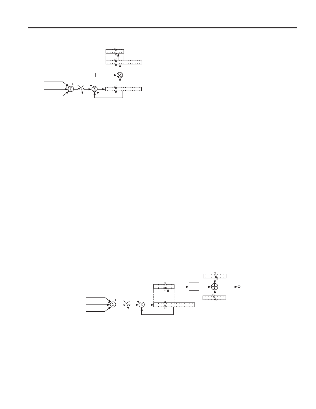
AN-624
POWER PHASE A
POWER PHASE B
POWER PHASE C
T
TOTAL
ACTIVE
POWER
AENERGY[23:0]
23
53
WDIV
53
0
0
0
Figure 8. Active Energy Accumulation
Active Power Pulse Output (CF)
The ADE7754 provides a pulsed output, CF, whose fre quency is proportional to the active power. It provides
a simple, single -wire, optically isolated interface to
external calibration equipment.
The energy-to-frequency conversion is accomplished
by accumulating the total active power in a 54-bit wide
register. An output pulse is generated each time the
register value is greater than 2
30
LSBs (see Figure 9).
The output frequency at CF, with full-scale ac signals
on all six channel inputs and CFNUM = CFDEN = 0x000,
is approximately 96 kHz. This can be calculated as follows:
with all the gain registers set to 0x000 (APGAINs,
WGAINs), the average value of the instantaneous active
power on each phase is 0xD1B717 or 13743895d. For all
three phases, the average value is 41231685d. An output
frequency is generated on CF when the internal register
accumulates 2
30
. The accumulation rate is CLKIN/4.
In the ADE7754, the CF frequency can be adjusted by
changing the different gain registers. As the ADE7754
is comprised of three independent inputs (phases), this
calibration needs to be done for each input independently. CFNUM and CFDEN are meant for global coarse
gain compensation and AWG, BWG, and CWG for fi ne
gain adjustment per phase.
Active Power Measurement
A solid state energy meter requires the display of the
active power in addition to the active energy. For 3-phase
applications, the requirement is generally for the display
of the active power per phase.
The ADE7754 does not provide a direct measurement
of the active power as defi ned in Equation 4, but instead
uses two accumulators for the active energy. Each
accumulator can be confi gured independently to hold
the active energy from a specifi c phase or the active
energy sum of several phases. One of the accumula tors (e.g., AENERGY) can be constantly used for the
regular total active energy accumulation (e.g., billing)
and the other accumulator (e.g., LAENERGY) can be
used for average active power measurement by dividing
the value read by the accumulation time.
Note: In the ADE7754, the average active power measurement per phase has to be processed one phase at a
time by changing the phase selected in the LAENERGY
accumulation. The switching between phases should
follow the descriptions of Figure 10 by changing the
MMODE and WATMODE register values.
CF Hz
()
Average Total Active Power CLKIN
=
30
×24
POWER PHASE A
POWER PHASE B
POWER PHASE C
×
TOTAL
ACTIVE
POWER
T
Figure 9. Energy-to-Frequency Conversion
(5)
CFNUM[11:0]
11
23
53
0
DFC
0
11
CFDEN[11:0]
0
CF
0
REV. 0
–5–
Page 6
AN-624
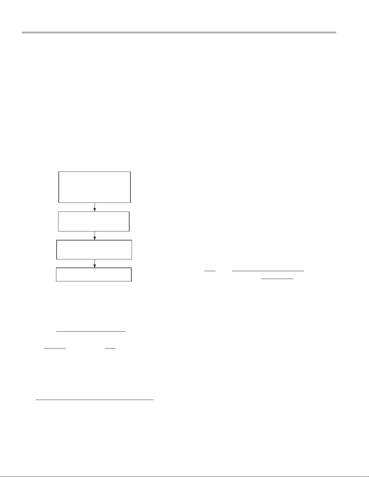
ACTIVE ENERGY GAIN CALIBRATION USING THE LAENERGY REGISTER
The ADE7754 accumulates the active power synchronously to the line cycles. This mode is especially useful
for calibration purposes as the ripple effect in the active
energy accumulation is reduced to zero (see the Line
Energy Accumulation section in the ADE7754 data sheet).
In this line accumulation mode, the ADE7754 accumulates the active power signal in the LAENERGY register
for an integral number of half line cycles. The number
of half line cycles, the phases selected to be accumulated, and the phases involved in the counting are
specifi ed in the LINCYC register, the LWATSEL bits of
the WATMODE register (address 0x0D), and in the
ZXSEL bits of the MMODE register (address 0x0B),
respectively. Figure 10 describes how to set up the line
accumulation mode in the ADE7754.
SET CONFIGURATION REGISTERS
ADDR. 0x0A – OPMODE
ADDR. 0x0B – MMODE
ADDR. 0x0D – WATMODE
ADDR. 0x18 – GAIN
SET NUMBER OF LINE CYCLES
TO 200
ADDR. 0x13 = 0d200
SET INTERRUPT MASK
FOR LINE ACCUMULATION
ADDR. 0x0F = 0x0400
The number of phases sele cted is the number of ones in
the ZXSEL bits of the MMODE register.
WDIV is a register used for scaling the active energy
accumulations; it does not affect the CF frequency. It is
introduced in Equation 6 to compensate its effect on
the LAENERGY value.
When calculating the expected CF frequency with a
LAE
NERGY reading and Equation 6, the actual ADE7754
register values used during the test should be used.
The CF frequency calibration has to be done for each
phase individually. The gain correction carried by the
CFNUM and CFDEN registers affects all three phases
similarly and should be used as a coarse gain compensation. The WG registers should then be used to fi ne
adjust the CF frequency to the expected frequency for
each individual phase.
Note: If the active power is accumulated in both the
active energy and line active energy registers during
the same amount of time, the line active energy register
value is four times the active energy register value.
Wh/LSB Constant Calibration
The active energy Wh/LSB constant and the CF frequency
can be calibrated at the same time using the line accumulation mode. Equations 6 and 7 detail the relationship
between the different parameters.
Under the steady load test condition, the watt power
consumption, W, is known. The Wh/LSB constant for the
AENERGY register is estimated using Equation 8 :
RESET INTERRUPT STATUS REGISTER
ADDR. 0x11
Figure 10. Line Accumulation Mode Setup
CF Frequency Gain Calibration
There is a direct relationship between CF frequency and
the line active energy register value (see Equation 6).
CF
(Hz) =
4 Accumulation Time(s)
CFNUM
×××+
CFDEN
×
WDIV 1
LAENERGY
WG
12
2
(6)
where Accumulation Time is the period of time during
which the active power has been accumulated in the
LAENERGY register:
Accumulation Time(s)
LINCYC
LineFrequency No. of Phases Selected
××
=
[15 0]2:
(7)
Wh
LSB
W Accumulation Time(s)
cst
×
=
LAENERGY
×3600
(8)
4
It should be noted that once the CF frequency has been
adjusted for each phase to the same value, the AENERGY
and LAENERGY registers will give the same value from
part to part and phase to phase under the same condi tions. Therefore, the Wh/LSB coeffi cient is a constant
that does not need to be calibrated. It can be estimated
by design and stored as is in the MCU.
Line Period Measurement
The calibration of the CF frequency and the Wh/LSB
constant with the line accumulation mode requires an
estimation of the line frequency. A poor estimation of
this quantity leads to errors in the calibration of the
system. Some calibration systems do not provide the
line frequency. The ADE7754 provides a measurement
of the line period in the period register (address 0x07).
The selection of the voltage input is done by Bits 0 and 1
–6–
REV. 0
Page 7

AN-624
of the measurement mode register
(address 0x0B). As
the resolution of the period register is 2.4 µs/LSB, the
Line Frequency in Equation 7 can be replaced by:
Line Frequency Hz =
()
Period Register s
1
2× .4 µ
(9)
Note: When selecting a voltage input for the ADE7754
period measurement, the same phase must be selected
for the zero-crossing detection (Bits 4 to 6 of the MMODE
register).
Active Power Gain Calibration
As explained previously, the active power information
per phase can be processed from the LAENERGY regis ter and the accumulation time. The conversion of the
LAENERGY register value to watts can be done by using
the Wh/LSB constant and the accumulation time as:
Average Active Power W
LAENERGY
4
Accumulation Time s
×
()=
3600
()
×
Wh LSB cst
/
As the phases’ gains should be balanced, the only
variables in this equation are the accumulation time
(depending on the period register) and the actual read ing from the LAENERGY register.
Note: In the ADE7754, the average active power measurement per phase has to be processed one phase at a
time by changing the phase selected in the LAENERGY
accumulation. The switching between phases should
follow the descriptions of Figure 10 by changing the
MMODE and WATMODE register values.
ACTIVE POWER OFFSET CALIBRATION USING THE LAENERGY REGISTER
An offset may exist in the power calculation due to
cross- talk between channels on the PCB or the IC itself.
The offset calibration allows the content of the active
power to be maintained at zero when no power is being
consumed.
To c omp e n s a t e for this error, a 2-point measurement is
needed. The measurement at the test current can be
used as well as another measurement at a lower current
level, e.g., I
/100. The APOS register is used to adjust
TEST
the result at low current input to the expected value processed from the I
TEST
value.
The calibration of the active power offset can be done
using the line active energy accumulation mode similar
to the gain calibration. If LAENERGY
and LAENERGY2
1
are the accumulation of the active power in the LAENER GY
register for two different current inputs (I1 and I2)
un
der the same conditions, e.g., the same number of line
cycles, frequency, voltage input, and gain, the offset to
be compensated is:
Offset
LAENERGY I – LAENERGY I
=
××
21 12
(10)
I–I
The offset of Equation 10 is an active energy offset. It
represents the number of LAENERGY LSBs that need
to be corrected. This number depends on the duration
of the accumulation.
An active power offset compensation is available in the
ADE7754, e.g., AAPOS for Phase A. During the active
energy accumulation, the value of this register is added
to the active energy every CLKIN/4. If the active energy
is accumulated during the accumulation time defi ned in
Equation 7, the APOS register is added to the LAENERGY
n times with:
n
where T
Accumulation Time(s)
=
×4
is the period of CLKIN.
CLKIN
T
CLKIN
S
()
(11)
The APOS offset is added to the 54-bit register dis played in Figures 8 and 9. An increment of one LSB in the
LAENERGY register happens only when n × APOS > 2
28
.
From Equations 10 and 11, the APOS offset value can
be set to:
APOS –
=×2
Offset
n
(12)
28
Note: If an error correction of 0.1% is desired, the active
energy accumulated in the line accumulation mode should
be greater than 1000 LSBs for both measurements.
PHASE CALIBRATION USING THE LAENERGY REGISTER
Phase matching between the current and voltage inputs
of a phase is a critical issue. The errors induced by phase
mismatch are minimal when PF = 1, but when PF = 0.5,
a phase error as small as 0.5° causes a 1.5% error in the
active power measurement.
Current transformers are very often used in 3-phase
applications. By design, they generate phase shifts varying from around 0.5° for a standard CT to values as
high as 5°. This phase shift must be compensated to
reduce the reading error at low power factor. The
ADE7754 has an internal phase compensation register
for each phase input that can be used for this purpose.
Each phase calibration register (APHCAL, BPHCAL, and
CPHCAL) can introduce a delay in the voltage channel’s
signal path from –19.2 µs to +19.2 µs.
To c alib rate thi s error, a 2-point measurement is needed.
Measurements at the test current, unity power factor,
and a lower power factor (e.g., 0.5) can be used. The
PHCAL register is used to adjust the result at PF = 0.5
to the expected value processed from PF = 1.
REV. 0
–7–
Page 8

AN-624
冪
The phase error is processed from the error between
these
two measurements:
Error
=
LAENERGY PF –
=
( 0.5)
LAENERGY PF
LAENERGY PF
2
=
(1)
=
(1)
(13)
2
The phase error is then:
Phase Error – arc sin
()3°=
Error
(14)
The phase register PHCAL is used to compensate for this
error. The operation held by the PHCAL register is a time
delay where one LSB is equivalent to 1.2 µs (CLKIN/12).
Depending on the line frequency of the voltage input, the
phase shift induced by the PHCAL register is different
(see Equation 15).
Phase
PHCAL Register . s
°=
××°×12 360
µ
1
PERIOD s()()
(15)
where PERIOD is the reading from the ADE7754 period
register for the specifi c phase.
From Equations 14 and 15, the value of the PHCAL register can be processed as:
arc sin
PHCAL Register
Error PERIOD s
3
=
×
2.4
°×
360 1.2µµ
(16)
s
Note: The equations above for phase calibration are only
valid for a test at PF = 0.5 inductive load only. If a test
at PF = 0.5 capacitive load is used, the sign of Equation 16
should be reversed.
Correction of Large External Phase Error
The PHCAL register can compensate only up to ±0.34°
at 50 Hz and ±0.41° at 60 Hz. If larger corrections are
re
quired, the larger part of the correction can be made
using external passive components. For example, the
resistors in the antialias fi lter can be modifi ed to shift the
corner frequency of the fi lter so as to introduce more or
less
lag. The lag through the antialias fi lter with 1 k⍀ and
33
nF is 0.56° at 50 Hz. Fine adjustments can be made
with the PHCAL register. Note that, typically, CT phase
shift does not vary signifi cantly from part to part. If a CT
phase shift is 1°, then the part-to-part variation should
be only about ±0.1°. Therefore, the bulk of the phase shift
(1°) can be cancelled with fi xed component values at the
design stage. The remaining small adjustments can be
made in production using the PHCAL registers.
RMS MEASUREMENTS
Theory of Operation
Root mean square (rms) is a fundamental measurement
of the magnitude of an ac signal. Its defi nition can be
both practical and mathematical. Practically, the rms
value assigned to an ac signal is the amount of dc
required to produce an equivalent amount of heat in
the same load.
Mathematically, the rms value of a continuous signal f(t)
is defi ned as:
F
=×∫()
RMS
1
T
2
ftdt
0
(17)
T
For signals in discrete time, rms calculation involves
squaring the signal, taking the average and then the
square root:
F
RMS
1
=×
f2i
∑
N
i
=
1
(18)
()
N
The method used to calculate the rms value in the
ADE7754 is to low-pass fi lter the square of the input
signal (LPF3) and take the square root of the result (see
Figures 11 and 12).
With V(t) =
2V sin (t), then
V(t) V(t) V – V t
×= ×
22
RMS RMS
cos (2 )ω
The low-pass fi lter (LPF3) attenuates the 2 component
2
of V
(t) and provides an average output proportional
to the square of the rms input (V
operation then provides V
RMS
2
). The square root
RMS
. The rms calculation is
simultaneously processed on the six analog input
channels. Each result is available in a separate register.
VRMSOS[11:0]
22212
24
0
VRMS
VOLTAGE
INPU T
SGN
LPF3
Figure 11. ADE7754 Voltage RMS Signal Processing
IRMSOS[11:0]
22212
0
24
IRMS
CURRENT
INPU T
SGN
LPF3
Figure 12. ADE7754 Current RMS Signal Processing
–8–
REV. 0
Page 9

AN-624
ADE7754 RMS Register Readings
As described earlier, the ADE7754 provides an rms measurement for each analog input every CLKIN/4. As the
low-pass fi ltering (LPF3) is not perfect, a ripple noise
coming from the 2 component is present in the rms
output (see the rms calculation in the ADE7754 data
sheet). To minimize the effect of this noise in the readings,
it is recommended to synchronize the rms readings
with the zero-crossing of the three input phases.
Figure 13 describes how to confi gure the ADE7754 for
this operation on Phase A.
SET CONFIGURATION REGISTERS
ZX SELECTED
ADDR. 0x0B – MMODE = 0x70
SET INTERRUPT MASK
FOR ZERO-CROSSING OF PHASE A + B + C
ADDR. 0x0F = 0x0380
RESET INTERRUPT STATUS REGISTER
RESET INTERRUPT STATUS REGISTER
ADDR. 0x11
INTERRUPT?
YES
READ VRMSA OR IRMSA
ADDR. 0x2C, 0x29
ADDR. 0x11
NO
Figure 13. ADE7754 RMS Reading Setup for Phase A
The VRMS and IRMS offset registers (VRMSOS and
IRMSOS) are used to adjust the low level input to match
the expected value derived from the high level value.
As the offset correction is implemented in a different
way for the voltage and current rms measurements
(see Figures 11 and 12), the processing of the adequate
correction is different for each channel.
Voltage Inputs RMS Offset Compensation
In the ADE7754, the voltage rms offset compensation
is performed after the square root as described in
Figure 11 and Equation 19.
VV VRMSOS
=+×64
RMS RMS0
(19)
The voltage rms offset compensation (VRMSOS) can
be processed from two nonzero measurements (see
Equation 20).
VV –V V
××1
RMS RMS
VRMSOS
where V
RMS1
=×
and V
without offset correction for input V
ly. V
and V2 must be expressed in any similar unit.
1
122 1
64
RMS2
V–V
21
are the rms register values
1
and V2, respective-
(20)
Current Inputs RMS Offset Compensation
In the ADE7754, the current rms offset compensation
is performed before the square root as described in
Figure 12 and Equation 21.
II IRMSOS
RMS2RMS
2
=+ ×
32768
0
(21)
The current rms offset compensation (IRMSOS) can be
processed from two nonzero measurements (see
Equation 22).
IRMSOS
where I
=×
32768
and I
RMS1
are the rms register values without
RMS2
offset correction for input I
2
II –I I
××1
RMS RMS
1
and I2, respectively. I1 and I2
1
222
I–I
221
2
2
1
2
(22)
must be expressed in any similar unit.
ADE7754 RMS OFFSET COMPENSATION
The rms calculation integrates any noise during its signal
processing. This noise contributes to the rms value as
a dc offset. The ADE7754 provides an offset compensation register for each rms measurement as described
in Figures 11 and 12.
To c ali b ra te out th is error, two nonzero measurements
are needed. As the dynamic range on the voltage channels and the current channels are different, these two
points are different. The voltage rms calculation provided in the ADE7754 is linear from full scale to full
scale/20 and the current rms calculation from full scale
to full scale/100. The two point measurements for the
voltage rms calculation can be V
NOMINAL
For the current rms measurement, I
and V
TEST
NOMINAL
and I
MAX
/10.
/100
can be selected.
REV. 0
SCALING OF ADE7754 RMS READINGS
A solid state energy meter requires the display of the
rms value of the analog inputs in a meaningful format,
e.g., amperes for current inputs and volts for voltage
inputs.
Therefore, the rms calculations processed in the ADE7754
need to be converted to volts or amperes by applying
a constant, e.g., V/LSB or A/LSB.
Due to sensor differences, the three analog inputs of
the same channel (voltage or current) do not generally
provide the same rms register value under the same
conditions. For this reason, each input rms measurement
needs a specifi c calibration parameter. As the ADE7754
does not provide individual gain calibration registers,
the conversion constant as well as the gain adjustment
need to be held in the MCU.
–9–
Page 10

AN-624
MCU RMS Scaling Adjustment Implementation
The ADE7754’s rms register value for a full-scale ac signal is around 1,848,772d. If 220 V represents half scale of
the analog input, the conversion constant is: 220/924,386
= 2.38 × 10
–4
V/LSB. The implementation of this gain
compensation can be done by multiplying the rms
register value from the ADE7754 by a 16- bit register
representing 2.38 × 10
multiplication is then divided by 2
–4
× 224 = 3993d. The result of this
24
(shif t right by 24 bit s)
to provide the voltage rms value in volts (see Figure 14).
INPUT (V) / RMS VALUE ⴛ 2
24
RMS
REGISTER
16
24
40
16
RMS DISPLAY
VALUE
24
2
Figure 14. Conversion of the RMS Register in
a Displayable Value
APPARENT POWER-ENERGY MEASUREMENTS
The apparent power is defi ned as the maximum active
power that can be delivered to a load. As V
RMS
and I
RMS
are the effective voltage and current delivered to the
load, the apparent power (AP) is defi ned as V
RMS
× I
RMS
Figure 15 shows the apparent power signal processing
implemented in the ADE7754 for each phase.
APPARENT POWER
SIGNAL – P
24
I
RMS
V
RMS
MULTIPLIER
24
24
12
VAG
Figure 15. Apparent Power Signal Processing
Apparent Energy Accumulation
A solid state energy meter very often requires the display of the amount of apparent energy consumed in
kVAh. When the ADE7754 is interfaced to a microcontroller (MCU), the MCU can read one of the apparent
energy registers, e.g., VAENERGY and LVAENERGY.
A full description of the functions of these registers can
be found in the ADE7754 data sheet. The total apparent
energy is accumulated in the ADE7754 by adding the
apparent powers from each phase and accumulating
them into the apparent energy register (see Figure 16).
APPARENT POWER
APPARENT POWER
APPARENT POWER
PHASE A
PHASE B
PHASE C
T
TOTAL
APPARENT
POWER
VAENERGY[23:0]
23
48
VADIV
48
0
0
0
Figure 16. Apparent Energy Accumulation
A VAh/LSB coefficient converting the value of the
VAEN ERGY or LVAENERGY registers to VAh should be
set. The calibration of this VA/ LSB const ant is described
in the Apparent Energy Gain Calibration Using
LVA ENERGY section.
Apparent Power Measurement
A solid state energy meter may require the display of
the apparent power per phase.
.
The ADE7754 does not provide a direct measurement
of the apparent power as defi ned by V
RMS
× I
RMS
, but it
provides two accumulators for the apparent energy.
Each accumulator can be confi gured independently to
hold the apparent energy from a specifi c phase or the
apparent energy sum of several phases. One of the
accumulators (e.g., VAENERGY) can be constantly used
for the regular total apparent energy accumulation (e.g.
billing) and the other accumulator (e.g., LVAENERGY)
can be used for the apparent power measurement by
dividing the value read by the accumulation time.
Note: In the ADE7754, the average apparent power
measurement per phase has to be processed one
phase at a time by changing the phase selected in the
LVAEN ERGY accumu lation. The switching between phases
should follow the descriptions of Figure 10 by changing
the MMODE and VAMODE (instead of WATMODE)
register values.
–10–
REV. 0
Page 11

AN-624
APPARENT ENERGY GAIN CALIBRATION USING THE LVAENERGY REGISTER
The ADE7754 accumulates the apparent power synchronously to the line cycles. This mode is especially useful
for calibration purposes as the ripple effect in the apparent energy accumulation is reduced to zero (see the Line
Energy Accumulation section in the ADE7754 data sheet).
In this line accumulation mode, the ADE7754 accumulates the apparent power signal in the LVAENERGY
register for an integral number of half line cycles. The
number of half line cycles, the phases selected to be
accumulated, and the phases involved in the counting are specifi ed in the LINCYC, the LWATSEL[2:0] bits
of the VAMODE register (address 0x0E), and in the
ZXSEL[6:4] bits of the MMODE register (address 0x0B),
respectively. Figure 10 describes how to set up the line
accumulation mode in the ADE7754 for the VA calculation. The confi guration of the WATMODE register can
be replaced by the confi guration of the VAMODE register
for the calibration of the apparent energy. The procedure
to calibrate Phase A is described in Figure 17.
SET ZERO-CROSSING PHASE DETECTION FOR LINE ACTIVE ENERGY
ACCUMULATION AND PHASE A FOR PERIOD MEASUREMENT
(MMODE REGISTER)
ADDR. 0x0B = 0x10 PHASE A
VAh/LSB Constant Calibration
The apparent energy VAh/LSB constant can be calibrated using the line accumulation mode. This constant
can be set by default to a nominal value. The nominal
value is determined during the design by experiment.
The purpose of the calibration is to adjust the VADIV
and VAG registers to get the same predetermined
LVA ENERGY accum ulation from all three phases.
Under the steady load test condition, the apparent
power consumption, VA, is known. The VAh/LSB constant is estimated using Equation 23:
VAh
LSB
VA Accumulation Time(s)
cst
×
=
3600 LVAENERGY
×
(23)
where Accumulation Time is given in Equation 7. As for
the active energy gain calibration, the accumulation
time in the line accumulation mode depends on the line
period (see the Line Period Measurement section).
The apparent gain calibration has to be done for each
phase individually. The gain correction carried by the
VAD IV r egister affects all three phases similarly and
should be used as a coar se g ain c ompen satio n. The VAG
registers should then be used to adjust the LVAENERGY
register to the expected value for each individual phase
(see Equation 24).
SET PHASE A FOR LINE ACTIVE ENERGY ACCUMULATION
(VAMODE REGISTER)
ADDR. 0x0E = 0x04 PHASE A
SET P HASE A INPUT
@ TEST VOLTAGE AND CURRENT
– OTHER PHASES INACTIVE
INTERRUPT?
YES
RESET INTERRUPT STATUS REGISTER
ADDR. 0x11
INTERRUPT?
YES
READ LVAENERGY REGISTER
ADDR. 0x06
READ PERIOD REGISTER
ADDR. 0x07
NO
NO
LVAENERGY
LVAENERGY
where LVAENERGY
××+
0
VADIV
is the line appar ent e nergy ac cumu -
0
=
1
1
VAG
12
2
(24)
lation without gain calibration, e.g., WG = VADIV = 0.
Apparent Power Gain Calibration
As explained previously, the apparent power information
per phase can be processed from the LVAENERGY register and the accumulation time. The conversion of the
LVAEN ERGY re gister value t o VA c an b e done by using
the VAh/LSB constant and the accumulation time as:
Average Apparent Power W
LVAENERGY
Accumulation Time
()=
VAh/LSB cst
×
As the phase gains should be balanced, the only variables in this equation are the accumulation time,
depending on the period register, and the actual reading
from the LVAENERGY register.
Note: In the ADE7754, the apparent power measurement
per phase has to be processed one phase at a time by
changing the phase selected in the LVAENERGY accumulation. The switching between phases should follow
the descriptions in Figure 10 by changing the MMODE
and VAMODE register values.
Figure 17. Apparent Energy Gain Calibration
Procedure for Phase A
REV. 0
–11–
Page 12

AN-624
ADE7754 CALIBRATION SOFTWARE
The ADE7754 calibration software is supported by
Windows
brate the watt, rms, and VA measurements of the
ADE7754. The software is designed to communicate
with the ADE7754 evaluation board via the parallel port
of a PC.
Installing the ADE7754 Calibration Software
The ADE7754 calibration software is supplied on one CD.
The minimum requirements for the PC are Pentium
233 MHz, 32 MB RAM, 10 MB free HD space, and at least
one PS/2 or ECP parallel port. To install the software,
place the CD in the CD drive and double - click setup.exe.
This launches the setup program that automatically
installs all the software components, including the unin stall program, and creates the required directories.
When the setup program has finished installing the
“AD E 77 5 4C al ” p r ogr a m, ins tr u ctions prompt the user to
install the National Instruments run-time engine. This
software was developed using National Instruments’
LabView
run the ADE7754Cal program. Follow the on- screen
instructions to complete the installation. To complete
the installation, the computer will need to be rebooted.
®
based software that allows the user to cali-
™
software; the runtime engine is required to
®
II
To l a un c h t h e s o ftware, go to Start ➞ Programs➞ADE7754
menu and select ADE7754Cal.
Uninstalling the ADE7754 Calibration Software
Both the ADE7754Cal program and the NI runtime
engine are easily uninstalled by using the Add/Remove
Programs facility in the Control Panel. Select the
pro gram to uninstall and click the Add/Remove button.
When installing a new version of the ADE7754 calibration software, the previous version should be
uninstalled.
Default Mode
When the software is launched, the user has the choice
to set the confi guration of the meter to either nominal
voltage, nominal current, line frequency, maximum current, minimum current, or meter constant for active
power pulse output (see Figure 18).
When the calibration is launched, each phase is calibrated for active power gain, offset, phase mismatch, rms
offsets, and apparent power gain. One phase is calibrated completely before going to the next phase. This
software should be used in conjunction with the
ADE7754 data sheet.
Figure 18. ADE7754 Calibration Default Window
–12–
REV. 0
Page 13

AN-624
ACTIVE ENERGY CALIBRATION
The ADE7754 calibration software manages the setup
of the ADE7754 and the calibration procedure. When
launched, a description of the next operation to perform or of the operation executed by the software is
provided. The new message is framed in a red box. Care fully read each message before going to the next step
of the calibration. The next step is carried out after
clicking the green Next button (see Figure 19).
Active Energy Gain Calibration
As explained, the fi rst step for calibration is to adjust
the CF frequency to a predetermined constant. On a
3-phase product, this gain calibration has to be done
on each phase separately to ensure correct gain balance
between phases. It is assumed in the following that
Phase A of the test equipment is connected to Phase A
of the ADE7754; the same is true for Phases B and C.
REV. 0
Figure 19. ADE7754 Calibration
–13–
Page 14

AN-624
The meter used as an example in this calibration procedure has three voltage sensors and three current
sensors. The gain calibration can be done with only
one test point. For a 220 V–30 A max meter, the test
point chosen is 220 V and 10 A. The meter constant is
6400 imp/kWh. The expected CF frequency in this case
is 220 × 10 × 6400/(1000 × 3600) = 3.911 Hz. The line
frequency in this example is 50 Hz.
The ADE7754 should be set in MODE0 for the active
energy calculation (WATMOD[7:6] = 00). Figure 20
shows the total active energy signal processing. The
gain calibration will be done by adjusting the AWG,
BWG, CWG, WDIV, CFNUM, and CFDEN registers.
AAPGAIN, BAPGAIN, and CAPGAIN are not used for
calibration in this mode.
WDIV and CFDEN are coarse gain adjustments for the
total active energy and CF pulsed output. AWG, BWG,
and CWG are fi ne gain adjustments for gain balancing.
For each phase, the active energy is accumulated
over 200 half line cycles in the LAENERGY register
(address 0x04). Only the calibrated phase is selected
for line counting (WATMOD[2:0] = 1, 2, or 4 depen ding
on the phase to calibrate).
Phase A: Active Energy Gain Calibration
All the registers are set to their default values, CFDEN
is set to 0, the MMODE register is set to 0x10, the
WATMODE register is set to 0x24, and Phase A current
and voltage inputs are active. Phase B and Phase C
inputs can be active as their contribution to the active
energy is disabled inside the part during this test.
Active energy is accumulated for 200 half lines cycles
and 38760d is read from the LAENERGY register. A
value of 8336d is read from the period register. Then,
using Equation 2, the CF frequency under this load is
calculated as:
CF HzHz()=
38760 2
=
4843.45
××
8336 2.4 10
4 200
××
×
1
×
1
–6
where WDIV = CFNUM = CFDEN = 0; accumulation
time = 2.0006 seconds.
Note: When WDIV, CFNUM, or CFDEN is equal to zero,
they are replaced by 1 in the calculation (see the
ADE7754 data sheet).
The desired frequency output under the test point
cho sen is 3.911 Hz. Therefore, the CF frequency must
be divided by 4843.45/3.911 = 1238.4d. This is achieved
by loading the CFDEN register with 1238d. This coarse
adjustment is valid for the calibration of all three
channels.
The fine adjustment of Phase A can be made using
the AWG register (address 0x19). CF varies with AWG
as described in:
With CF
CF CF
=×+
INITIAL
= 4843.45 Hz, CFNUM = 0, and CFDEN =
INITIAL
AWG CFNUM
×1
12
CFDEN
2
123 8d, AWG should be set to correct the mismatch
between the target frequency (3.911 Hz) and the initial
frequency. In this example, AWG should be set to –1d
or 0xFFF.
In this example, the Wh/LSB can be processed using
Equation 8:
Wh
LSB
×××
4 220 10 2.0006
=
××
3600 38760 1 –
=×
1.262 10
1
12
2
–4
This constant is the same for all three phases. It should
be noted that the resolution of the AENERGY register
can be changed with the WDIV register. Increasing
WDIV will reduce the reading out of the AENERGY register and, therefore, increase the Wh/LSB constant
proportionally.
The procedure to calibrate Phase A is described in
Figure 21.
PHASE A
PHASE B
PHASE C
HPF
I
A
AAPGAIN
V
A
I
B
BAPGAIN
V
B
I
C
CAPGAIN
V
C
HPF
1
HPF
1
BAPOS
28
1
28
28
AAPOS
BWGAIN
CAPOS
AWGAIN
LPF2
CWGAIN
LPF2
TOTAL INSTANTANEOUS
POWER SIGNAL
LPF2
ADE7754
WDIV
CFNUM
CFDEN
ACTIVE ENERGY
REGISTER
CF
Figure 20. Total Active Energy Calculation
–14–
REV. 0
Page 15

AN-624
SET ZERO-CROSSING PHASE DETECTION
FOR LINE ACTIVE ENERGY ACCUMULATION
AND PHASE A FOR PERIOD MEASUREMENT
(MMODE REGISTER)
ADDR. 0x0B = 0x10 PHASE A
LINE ACTIVE ENERGY ACCUMULATION
RESET INTERRUPT STATUS REGISTER
SET PHASE A FOR
(WATMODE REGISTER)
ADDR. 0x0D = 0x024 PHASE A
SET PHASE A INPUT
@ TEST VOLTAGE AND CURRENT
– OTHER PHASES INACTIVE
INTERRUPT?
YES
ADDR. 0x11
INTERRUPT?
YES
READ LAENERGY REGISTER
ADDR. 0x03
READ PERIOD REGISTER
ADDR. 0x07
SET CFDEN AND AWG REGISTERS
ADDR. 0x26 AND 0x19
NO
NO
Figure 21. Active Energy Gain Calibration Procedure
for Phase A
Phase B: Active Energy Gain Calibration
All the registers are set to their default values, CFDEN
is set to 1238d, the WATMODE register is set to 0x12, the
MMODE register is set to 0x21, and Phase B current and
voltage inputs are active. Phase A and Phase C inputs
can be active because their contribution to the active
energy is disabled inside the part during this test. Active
energy is accumulated for 200 half line cycles and 38631d
is read from the LAENERGY register. A value of 8336d
is read from the period register. Then, using Equation 6,
the CF frequency under this load is calculated as:
1
××
×
×
1
–6
×
1
1238
CF HzHz()=
38631 2
=
3.8993
××
8336 2.4 10
4 200
where CFNUM = 0 and CFDEN = 1238d.
The desired frequency output is 3.911 Hz with Phase B
active only.
The fine adjustment of the output frequency can be
made using the BWG register (address 0x1A). CF varies
with BWG as described in Equation 4, replacing AWG
by BWG.
With CF
= 3.8993 Hz, CFNUM = 0, and CFDEN =
INITIAL
123 8d, BWG should be set to correct the mismatch
between the target frequency (3.911 Hz) and the initial
frequency. BWG should be set to 13d or 0x000D in this
example.
Phase C: Active Energy Gain Calibration
All the registers are set to their default values, CFDEN
is set to 1238d, the WATMODE register is set to 0x09,
the MMODE register is set to 0x42, and Phase C current
and voltage inputs are active. Phase A and Phase B
inputs can be active because their contribution to the
active energy is disabled inside the part during this test.
Active energy is accumulated for 200 half lines cycles
and 38687d is read from the LAENERGY register. Following the same procedure as for Phase B, the CWG
register should be adjusted to 7d to reach the expected
CF frequency.
Active Power Offset Calibration
As explained previously, the calibration of the active
power offset can increase the performance of the energy
meter over the current dynamic range. In the example
used in this document, the minimum current is 10 mA
for a maximum current of 30 A and a reference current
of 10 A.
Phase A: Active Power Offset Calibration
Using the previous setup as a reference, 38760d is read
from the LAENERGY register at I
(10 A) with 200
REF
half line cycles. At 10 mA under the same conditions,
the accumulation in the LAENERGY register would
be around 38d if no offset were present. A value of
38d is too small to make an accurate offset compen sation calculation where an accuracy of at least 0.1%
is needed. With 38d, the resolution error is already
2.6%/LSB in the reading itself. It is necessary to use a
larger number of half line cycles to get a larger value
from the LAENERGY accumulation at low current.
To g e t e nough resolution for the active power offset
compensation, a lower limit of 2000d for the LAENERGY
accumulation at low current is fi xed in the ADE7754
calibration software, i.e., resolution of 0.05%/LSB.
In our example, the number of half line cycles necessary
to get this value is: LINCYC = 2000/(38760/10 × 0.01) ×
200 = 10320. The accumulation time in this case is roughly
10320/2/50 = 103 seconds.
Under the same conditions as for the Phase A gain
calibration with LINCYC = 10320d, the LAENERGY
accumulation read from the ADE7754 is 2041d.
REV. 0
–15–
Page 16

AN-624
As the two line active energy accumulations use different accumulation time and the second measurement
is done after gain calibration, it is necessary to scale
the fi rst measurement (at 10 A) to the value it would
be with LINCYC = 10320 and to AWG = –1:
LAENERGY1 = 38760 × 10320 × (1 – 1/2
= 10; I2 = 0.01; LAENERGY2 = 2041d; PERIOD = 8336d
I
1
From Equation 10: Offset = 41d
From Equation 11: n = 258082560d
then AAPOS = – 43d = 0xFD5.
Figure 22 shows the active energy accuracy performances of a meter with and without watt offset
compensation.
6.0
5.0
4.0
WITHOUT OFFSET COMPENSATION
3.0
2.0
ERROR (%)
1.0
0
WITH OFFSET COMPENSATION
–1.0
0.01
CURRENT CHANNEL (A)
Figure 22. Active Energy Linearity Errors
Note: This calibration step can take a large amount of
time due to the accumulation time needed for an accurate measurement of the active energy at low current.
The user can decide the minimum current in the fi rst
window of the ADE7754 calibration software. This min imum current is used as the low end point of the active
energy offset calibration. Increasing this value will
reduce the calibration time. Depending on the resolution needed at low current, a minimum of 2000 LSB for
the LAENERGY accumulation might not be necessary.
In the ADE7754 calibration software, the user can
change the number of li ne cyc les for the next LAENERGY
accumu lation (Figure 23). The value proposed in the
window correspond to an approximate LAENERGY
accumula tion of 2000 LSB under the conditions specifi ed.
12
)/200 = 1999528d.
1.00.1
10
Figure 23. Change LINCYC Register for Offset Calibration
Phase B and C: Active Power Offset Calibration
The watt offset calibration of Phase B and Phase C can
be done the same way using the ADE7754 calibration
software. The confi guration of the ADE7754 for each
phase is the same as the one used for the gain calibra tion for the same phase.
Phase Calibration
As explained previously, phase mismatch between voltage and current inputs can create a large error in the
watt measurement at low power factor. In the ADE7754
calibration software, the phase error calibration is done
by using the first measurement collected for watt
gain calibration and by doing another measurement at
PF = 0.5 with inductive load (voltage leading current).
As for the watt gain calibration, the active energy is
accumulated over 200 half line cycles in the LAENERGY
register (address 0x04) for each phase. Only the calibrated phase is selected for line counting (WATMOD[2:0] =
1, 2, or 4, depending on the phase to calibrate).
Phase A: Phase Calibration
The setup is the same as for the Phase A gain calibration. Phase A current and voltage inputs are active with
a PF = 0.5 (inductive load). Active energy is accumulated
for 200 half line cycles and 19442d is read from the
LAENERGY register. A value of 8336d is read from the
period register. As the first measurement (for gain
calibration) has been done without gain compensation
and the second measurement with it (AWG = –1), the
first measurement has to be compensated for this
change: 38760 × (1 – 1/2
12
) = 38750.5.
The error given by Equation 13 is then 0.344% or 0.11°.
Using Equation 16, the phase calibration register (APHCAL)
is calculated as:
×
APHCAL =×
8336 2.4
360 1.2
°×
s
=– 0.11
–5
s
–16–
REV. 0
Page 17

AN-624
Phase B and C: Phase Calibration
The phase calibration of Phase B and Phase C can be done
the same way, using the ADE7754 calibration software.
The configuration of the ADE7754 for each phase is
the same as the one used for the gain calibration for the
same phase.
RMS CALIBRATION
The ADE7754 provides six rms measurements for the six
analog inputs. These rms calculations have to be calibrated for offset to give an accurate measurement at
low levels. The ADE7754 provides rms offset correction
registers for each rms measurement.
The ADE7754 does not provide rms gain correction.
As explained before, the rms gain calibration has to be
done in the MCU. The ADE7754 calibration software
provides the calibration constants (V/LSB and A/LSB)
that can be used in the MCU for conversion of the rms
register values to the actual inputs.
Figures 24 and 25 show the difference with and without rms offset compensation for the voltage and current
inputs.
1.4
1.2
1.0
0.8
0.6
ERROR (%)
0.4
0.2
0.0
–0.2
10
WITHOUT OFFSET COMPENSATION
WITH OFFSET COMPENSATION
100 1k
VOLTAGE CHANNEL (V)
Figure 24. Voltage RMS Linearity Errors
2.0
1.0
0
–1.0
–2.0
ERROR (%)
–3.0
–4.0
WITH OFFSET COMPENSATION
WITHOUT OFFSET COMPENSATION
RMS Offset Calibration
Phase A: RMS Offset Calibration
All the registers are set to their default values, except
CFDEN, AWG, APHCAL, and AAPOS, which are set to
their calibrated values. The MMODE register is set to
0x70 (ZXSEL Phase A, Phase B, and Phase C enabled),
the MASK register is set to 0x0380 (Z XA, ZXB, ZXC interrupts enabled only).
Phase A current input is set to its reference value (10 A)
and Phase A voltage input is set to its nominal value
(220 V). Voltage and current rms Phase A registers
(address 0x2C and 0x29, respectively) are read as
described in Figure 13 and averaged over 500 samples:
VRMS1 = 1019627d and IRMS1 = 436988d.
Note: In the ADE7754 calibration software, these measurements are done during the watt gain calibration.
Under the same conditions, the voltage and current
inputs are changed to V
NOMINAL
/10 (22 V) and I
MAX
/100
(0.3 A). The voltage and current rms phase A registers
are read as described in Figure 13 and averaged over
500 samples: V
= 102246d and I
RMS2
= 14059d.
RMS2
Based on these measurements, the voltage rms offset
and current rms offset register values can be processed
using Equation 20 and 22:
AVRMSOS =
164220 102246 – 22 1019627
××
×
22 – 220
=
–5
AIRMSOS =
222 2
1
32768
××
10 14059 – 0.3 436988
×
22
0.3 – 10
=
– 788
The V/LSB and A/LSB constant can be processed from
the measurements at 220 V and 10 A:
Phase A V/LSB = 220/1019627 = 2.158 × 10
Phase A A /LSB = 10/436988 = 2.288 × 10
–4
–5
Phase B: RMS Offset Calibration
All the registers are set to their default values, except
CFDEN, BWG, BPHCAL, and BAPOS, which are set to
their calibrated values. The MMODE register is set
to 0x71 (ZXSEL Phase A, Phase B, and Phase C enabled).
The MASK register is set to 0x0380 (ZXA, ZXB, ZXC
interrupts enabled only).
The two measurements at 220 V–10 A and 22 V–0.3 A
can be done in the same manner as for Phase A and will
lead to the calculation of BIRMSOS, BVRMSOS, Phase B
V/LSB, and Phase B A/LSB values.
REV. 0
–5.0
0.1
CURRENT CHANNEL (A)
Figure 25. Current RMS Linearity Errors
100101.0
–17–
Page 18

AN-624
T
Phase C: RMS Offset Calibration
All the registers are set to their default values, except
CFDEN, CWG, CPHCAL, and CAPOS, which are set to
their calibrated values. The MMODE register is set to
0x72 (ZXSEL Phase A, Phase B, and Phase C enabled).
The MASK register is set to 0x0380 (ZXA, ZXB, ZXC
interrupts enabled only).
The two measurements at 220 V–10 A and 22 V–0.3 A
can be done in the same manner as for Phase A and will
lead to the calculation of CIRMSOS, CVRMSOS, Phase C
V/LSB, and Phase C A/LSB values.
APPARENT ENERGY GAIN CALIBRATION
As explained in the ADE7754 data sheet, each compo nent of the apparent calculation (V
RMS
and I
) is offset
RMS
calibrated, so the apparent power measurement does
not need to be offset calibrated.
The gain calibration of the apparent power measure ments has two steps:
1. C alibr a te the apparent power to a nominal value
determined by design.
2. Calibrate the apparent power per phase to the same
value (phase balancing).
In the ADE7754 calibration software, no predetermined
value is set. The software will select the fi rst apparent
energy value read from the fi rst phase calibrated as
a reference and will change the VAG registers of the
other phases to match this value. This method differs
from the gain calibration for the active power where
a predetermined value is set by the meter constant
imp/kWh.
The ADE7754 should be set in MODE0 for the apparent
energy calculation (VAMOD[7:6] = 00). Figure 26 shows
the total apparent energy signal processing. The gain
calibration will be done by adjusting the AVAG, BVAG,
CVAG, and VADIV registers. AAPGAIN, AVAG AIN,
BAPGAIN, BVGAIN, CAPGAIN, and CAVGAIN are not
used for calibration in this mode.
VAD IV i s the c oarse gain adjustment for the total
apparent energy. AVAG, BVAG, and CVAG are fi ne gain
adjustments for gain balancing.
For each phase, the apparent energy is accumulated
over 200 half line cycles in the LVAENERGY register
(address 0x06). Only the calibrated phase is selected
for line counting (VAMOD[2:0] = 1, 2, or 4, depending
on the phase to calibrate).
RMS
RMS
RMS
RMS
RMS
RMS
24
AVAGAIN
24
BVAGAIN
24
CVAGAIN
TOTAL APPAREN
POWER SIGNAL
PHASE A
PHASE B
PHASE C
V
V
V
I
A
A
I
B
B
I
C
C
AAPGAIN
AVGAIN
BAPGAIN
BVGAIN
CAPGAIN
CVGAIN
Figure 26. Total Apparent Energy Application
Phase A: Apparent Energy Gain Calibration
All the registers are set to their default values, the
MMODE register is set to 0x10, the VAMODE register is
set to 0x24, and only Phase A current and voltage inputs
are active. Phase B and Phase C inputs can be active
since their contribution to the apparent energy is disabled inside the part during this test. Apparent energy
is accumulated for 200 half line cycles and 10582d is
read from the LVAENERGY register. A value of 8336d
is read from the period register. The value from the
LVAEN ERGY re gister is used as the reference value for
the gain calibration.
Accumulation time = 2.0006 seconds.
In this example, the VAh/LSB constant can be processed
using Equation 23:
VAh
LSB
cst =
××
220 10 2.0006
×
3600 10582
=×
1.1554 10
–4
This constant is the same for all three phases. It should
be noted that the resolution of the VAENERGY register
can be changed with the VADIV register. Increasing
VADIV will redu ce the reading out of the VAENERGY
register and, therefore, increase the VAh/LSB constant
proportionately.
–18–
REV. 0
Page 19

AN-624
Phase B: Apparent Energy Gain Calibration
All the registers are set to their default values, the
VAMODE regis ter is set to 0x12, the MMODE register is
set to 0x21, and only Phase B current and voltage inputs
are active. Phase A and Phase C inputs can be active
because their contribution to the apparent energy is
disabled inside the part during this test. Apparent energy
is accumulated for 200 half line cycles and 10558 is read
from the LVAENERGY register. A value of 8336d is read
from the period register. The expected value for this
register is 10582 (from Phase A measurement). The fi ne
adjustment of the LVAENERGY register value can
be made using BVAG register (address 0x1D). The
LVAEN ERGY re gister value varies with BVAG as
described in Equation 24.
With LVAENERGY0 = 10558, VADIV = 0, BVAG should
be set to correct the mismatch between the target
register value (10582) and the actual measurement.
BVAG should be set to 9d or 0x0009 in this example.
Phase C: Apparent Energy Gain Calibration
CVAG (address 0x1E) is set to its default value, the
VAMODE regis ter is set to 0x09, the MMODE register is
set to 0x42, and only Phase C current and voltage inputs
are active. Phase A and Phase B inputs can be active
as their contribution to the apparent energy is disabled
inside the part during this test. Apparent energy is
accumulated for 200 half lines cycles and 10571d is read
from the LVAENERGY register. Following the same
procedure as for Phase B, the CVAG register should be
adjusted to 4d to reach the expected LVAENERGY register value.
REV. 0
–19–
Page 20

E03546–0–4/03(0)
© 2003 Analog Devices, Inc. All rights reserved. Trademarks and registered trademarks are the property of their respective companies.
–20–
 Loading...