

Page 1
AN-593
16
15
14
13
12
11
10
9
1
2
3
4
5
6
7
8
VID0
VID1
VID2
VID3
LRFB1
LRDRV1
CS–
CS+
GND
DRVH
DRVL
VCC
LRFB2
LRDRV2
COMP
CT
FROM CPU
C1
100F
C15
1F
C13
100F
Q2
*
C12
1F
Q1
*
C3
150pF
R
B
10.5k⍀
R
A
78.7k⍀
C
OC
2.7nF
3.3V
C17 C18 C19C20 C21
V
LR2
1.5V,
2A
R12
4m⍀
L1
1.7H
Q3
SUB75N03-07
C8
1000F
C9
1000F
C7
22F
L2
1H
VCC CORE
1.30V TO
2.05V
15.1A
5V
5V STANDBY
12V
D3
MBR052LT1
D2
MBR052LT1
V
LR1
2.5V, 2A
C6
1F
R4
220⍀
R3
220⍀
C10
1nF
3.3V
ADP3178
+++++
+++
+
+
+
*
SUB45N03-13L
C2
68pF
C11
68pF
R2
24.9k⍀
R11
13.3k⍀
1000F ⴛ 5
RUBYCON ZA SERIES
24m⍀ ESR (EACH)
R1
16.9k⍀
R10
26.7k⍀
Q4
SUB45N03-13L
a
APPLICATION NOTE
One Technology Way • P.O. Box 9106 • Norwood, MA 02062-9106 • Tel: 781/329-4700 • Fax: 781/326-8703 • www.analog.com
Stability and Transient Analysis of the Miller-Compensated
Linear Regulators on the ADP3178
By Jeritt Kent and Joe Buxton
Analog Devices’ power management group has been in
the desktop computer VRM controller market since the
mid-90s. The ADP3158 programmable synchronous
buck converter was positioned to fit into designs conforming to Intel’s VRM 8.4 specifications. Designers
typically used the ADP3158’s buck converter for the CPU
core switching supply and its two integrated fixed linear
regulators to generate additional system voltages. In
one major application, the ADP3158 linear regulators
were used for generating a 2.5 V, 4.3 A DDR VDDQ supply and the 1.5 V, 1.5 A GTL supply. In order to generate
the 1.5 V supply, designers used the 1.8 V linear regulator, driving its inverting input with the output of the 2.5 V
regulator through an R
1.8 10 / 7 –2.5 3 / 7 1.5
() ()
This approach added a minor tolerance error and noise
component to the resultant 1.5 V supply. Additional
compensation was added to control loop disturbances
initially thought to be sympathetic to the frequency of
the switching supply. Unfortunately, these techniques
did not optimize performance of both the loop stability
and overall transient response. Design using the
ADP3178 resolves these issues. The on-board references
of the ADP3178 are now based on a 1.0 V reference versus
the 1.8 V and 2.5 V references on the ADP3158.
ratio of 3/7:
f/Rin
= V
REV. 0
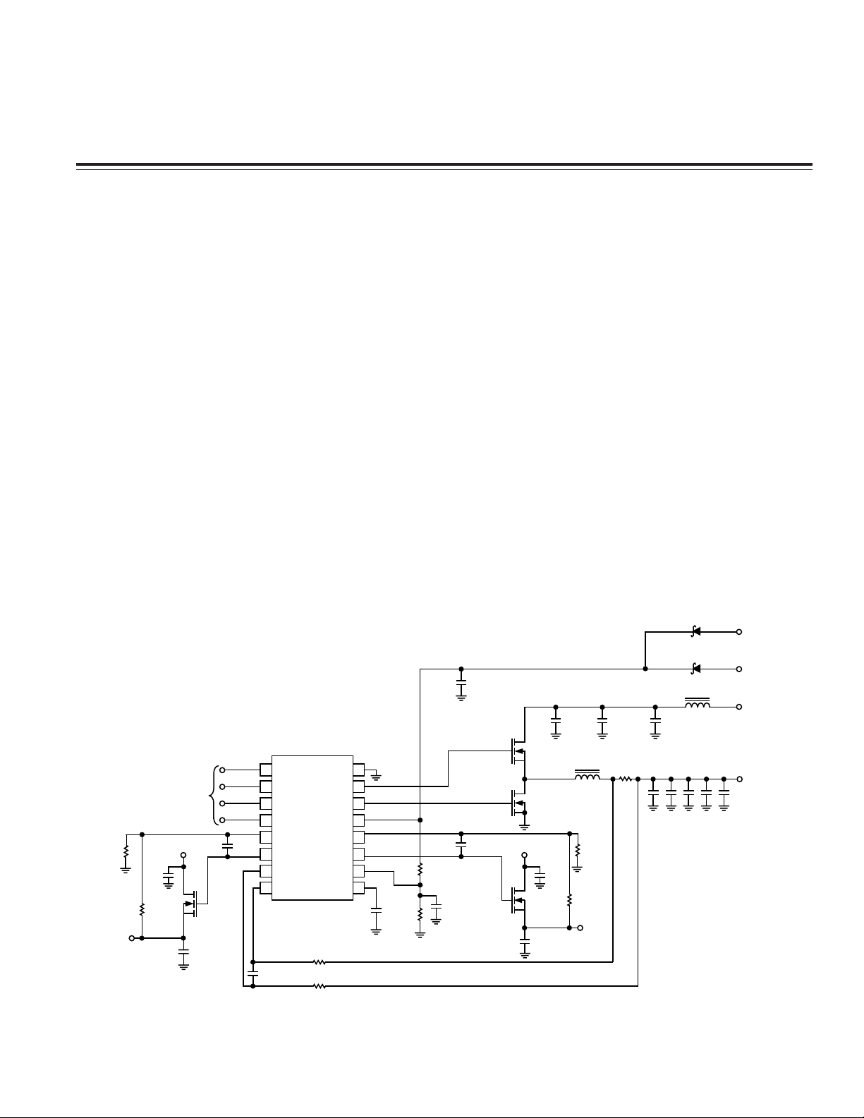
Figure 1. Complete Implementation of the ADP3178
© Analog Devices, Inc., 2002
Page 2

AN-593
Figure 1 shows a complete implementation of the
ADP3178. Whereas the ADP3158 linear regulators use a
fixed 10 kΩ resistor, the ADP3178 uses voltage dividers
in the feedback. Equations 32 and 33 of the ADP3178
data sheet provide the calculations for these resistor
sizes. Figure 1 shows standard 1% resistors that
approximate a 10 kΩ equivalent for both 2.5 V and 1.5 V
supplies. The output voltage can be easily set from 1.0 V to
within V
tied to the drain of the external N-channel MOSFET. In
addition, the lower on-board reference voltages on the
ADP3178 versus the ADP3158 allow for better noise
immunity for sub 1.8 V output voltage requirements.
Miller compensation is used for the ADP3178 design.
The open-loop gain,
ers on the ADP3178 from simulation is approximately
450 V/V (see Figure 2). Taking advantage of this gain, a
relatively small compensation capacitor can be placed
in the feedback of the linear regulator amplifier from
LRFB to LRDRV. This capacitor, along with the parallel
combination of the resistive voltage divider used to set
the output voltage, sets the dominant pole for the linear
regulator loop via the equation:
where
open-loop gain of the linear regulator amplifier,
MOSFET gate capacitance (2.7 nF for the SUB45N0313L), and
divider).
The dominant pole location should be set to roll off the
open-loop gain of the amplifier to 0 dB at approximately
the same point as the second pole comes into the picture. The output impedance of the MOSFET and the load
capacitance set the second pole. The MOSFET shown in
the ADP3178 data sheet is the SUB45N03-13L. The method
for selecting a MOSFET for a particular application
should be driven by power dissipation requirements.
It should also have a logic level V
In addition, selection of a MOSFET with lower Qg (gate
charge) will improve the transient response and slew
rate. Ideally, one would use a drain supply voltage
sufficiently above the required output voltage to give
headroom on V
keeping the power dissipation to a minimum.
The 4.3 A requirement on the 2.5 V DDR VDDQ supply
would give a maximum power dissipation figure of
0.8 × 4.3 = 3.44 W given a 3.3 V supply. That figure can be
(for the required load current) from the supply
ds
A
, of the linear regulator amplifi-
V
P1/2 C A C R
=×××
dmVgf
C
is the Miller compensation capacitor,
m
R
is R1储R2 (the resistors used in the voltage
f
π
()
()
for a required output current while
ds
()
+
×
A
V
C
g
for easier drive.
th
is the
is the
dropped to 2.15 W if a 3 V drain supply is available. After
selecting a MOSFET and package capable of handling
the power, one should check the transconductance, g
For example, the SUB45N03-13L has a g
for a 1 A load current.
Because the output capacitance of the MOSFET is very
small compared to the load capacitance, the second
pole for this Miller configuration can be simplified to:
P1/2 R R C
=×××
2OESR L
Where
capacitance in this paper is meant to describe the physical capacitor placed between the source of the MOSFET
and analog ground.
Some authors refer to the sum of the capacitances
driven by the MOSFET’s source as the bypass capacitance, C
load capacitance. For example, if the linear regulator
drives the supply voltage for five other devices, each of
which locally bypasses VDD to VGND through the typical 0.1 µF ceramic capacitor (ESR is negligible for these
capacitors), this bypass capacitance would be only 0.5 µF
versus, say, a 10 µF load capacitance. The pole contributed by the bypass capacitance for this compensation
approach is usually well beyond the “zone of concern.”
For example, if the load capacitor is a 10 µF MLCC (with
an ESR of around 10 mΩ) and the SUB45N03-13L
is used, the second pole lands at 208 kHz. The pole contributed by 0.5 µF of bypass capacitance is around
32 MHz, as:
Given a constant gain-bandwidth product for this voltage feedback circuit, a dominant pole location near
P
through unity gain at 208 kHz. Figure 2 illustrates the
frequency response. Using a value of 10 kΩ for Rf, C
would be about 71 pF, per the equation for Pd above.
68 pF is the closest standard value, as seen in Figure 1.
Given that the ADP3178 requires a feedback voltage of
1.0 V, the 10 kΩ equivalent feedback resistance for generating 2.5 V would be R
resistor in Figure 1) and R
ground). The Thevenin value of 10 kΩ is a convenient
value and can be changed (which also changes C
However, it should not be made too large due to the
input bias current of the linear regulator.
CL
is the load capacitance and
. This value is typically smaller than that of the
BP
P1/2 R C
3 ESR BP
= 208 kHz/450 = 462 Hz is needed in order to cross
2/AV
π
()
=×××
()
π
()
= 25 kΩ (replacing the 10 kΩ
1
= 16.7 kΩ (tied from LRFB to
2
of 15 Siemens
m
×
R
= 1/gm. Load
O
m
m
.
m
).
–2–
REV. 0
Page 3

AN-593
–20
–40
–60
–80
–100
–120
200
150
100
–50
–100
–150
–200
60
40
20
0
50
0
0.1
0.1
110
110
100 1e3 1e4 1e5 1e6 1e7 1e8
FREQUENCY – Hz
100 1e3 1e4 1e5 1e6 1e7 1e8
FREQUENCY – Hz
VdB (OUT) –VdB (fb)
Vp (OUT) –Vp (fb)
Figure 2. AC Gain/Phase Plot
The equivalent model for the load capacitance is difficult
to determine exactly because it depends on the ESR of
the capacitance as well as the layout. For example, if
instead of a 10 µF MLCC for the load capacitor, a bulk
capacitor of 100 µF and 0.5 Ω ESR were used, the second
pole of this system would be at 2.8 kHz. The zero, also a
function of the bulk capacitor’s ESR, is at 3.2 kHz via:
Z1/2 C R
=×××
π
()
L ESR
Since both of these transitions occur close together and
well before (nearly two decades) the 208 kHz critical
point, they act to “cancel” one another. Thus the bulk
capacitor will not have a significant effect on the loop
response of the linear regulator at crossover. Also, if
several high frequency capacitors are connected in parallel (along a bus on the linear regulator’s output, for
example), the ESR of these capacitors located away
from the linear regulator’s output will be higher due to
board parasitics. This will only push the zero closer to
the second pole. So, fortunately for the ADP3178 design,
these “distant” capacitors will maintain their preferable
local bypass effect, but will not affect stability. However,
because of this uncertainty in the load characteristics, it
is still important to verify the operation in the actual
application. If the output shows instability under any
load conditions, C
should be increased.
m
The linear regulator cannot instantaneously respond to
a transient condition. There is some fixed delay time before the MOSFET can handle the increased load current.
During this time, the load capacitor has to handle the full
transient load. The ESL (equivalent series inductance) of
the load capacitor and its layout, while usually quite
small, can have an impact where design specifications
call out a high ␦i/␦t. To keep the ESL low, place the MOSFET and the load capacitor as close as possible to the
linear regulator. In addition, one should consider using
a plane for the linear regulator output and its return path.
The next question to ask when selecting the load capacitor is: ”Is the ESR low enough for a transient load step?”
If the specification allows for a 100 mV droop for a 1 A
current step, then the ESR should obviously be less than
100 mΩ. The second consideration is the total charge
and allowable droop. After the ESR step, the capacitor
has to supply the load current until the linear regulator
can catch up.
The larger the dip in the output voltage, the greater the
differential voltage seen on the inputs of the linear regulator amplifier; thus a greater MOSFET drive current. So
the linear regulator responds faster in circuits with
larger ESR values; the ESR droop period decreases as
the ESR increases. Optimal transient performance
would mandate a minimum ESR, which in many alternate designs would compromise stability. This is a
primary advantage of the ADP3178. As discussed earlier, the ADP3178 does not rely on load capacitor ESR for
stability (the pole and zero created by the ESR tend to
cancel one another).
The dip in output voltage can be translated to the output
of the amplifier via A
, where the output drive current is
V
governed by the amplifier’s small signal output impedance (measurements show it on the ADP3178 to be
typically around 100 kΩ with a range of 75 kΩ to 150 kΩ).
For a 10 µF MLCC load capacitor, as discussed previously, the unity gain crossover point was calculated as
208 kHz. The closed-loop response of this system must,
therefore, be greater than 1/208 kHz or 4.8 µs. The simulations in Figure 3 are consistent.
REV. 0
–3–
Page 4

AN-593
2.54
V
OUT
2.52
2.50
2.48
2.46
2.44
2.42
2.40
2.38
0
510152025303540 455055
1.40
I (I
LOAD,
1.20
1.00
0.80
0.60
0.40
0.20
TIME – XLE-6 Seconds
P)
I (I
SOURCE
, P)
For this example, the V
graph of Figure 3 shows a
OUT
slope of about –100 mV/µs. The linear regulator amplifier will respond to an attenuated version of this at its
input—40 mV/µs for an output voltage of 2.5 V and reference voltage of 1 V as on the ADP3178. The amplifier’s
negative feedback attempts to force its inputs equal by
driving its output more positive. The response of the
system takes advantage of the “pull-apart” drive on the
MOSFET—i.e., the amplifier is driving the gate higher,
while the load capacitor discharge is pulling the source
lower. V
MOSFET drain current managed by g
thus increases relatively quickly, as does the
gs
= Id/Vgs.
m
Of interest is the fact that the ADP3178’s output drive
current is about four times greater than that of the
ADP3158 (it is limited to about 2 mA), but will likely have
an advantage only for MOSFETs with very high gate capacitance or very small transconductances. Therein lies
another factor beyond power dissipation for MOSFET
selection. It is clear from the V
Figure 3, estimating
␦
V
/␦t
to be about 60 mV/µs, that
GATE
graph in
GATE
the amplifier’s drive current is nonlimiting, as:
=×
IC Vt
DRIVE GATE GATE
δδ
()
/
E02981–0–8/02(0)
0
0
51015202530 3540455055
5.3
V
GATE
5.2
5.1
5.0
4.9
4.8
4.7
0
510152025303540 455055
TIME – XLE-6 Seconds
TIME – XLE-6 Seconds
Figure 3. Transient Response with 10 µF MLCC Output
Capacitor
Another way to examine this closed loop is from a voltage standpoint (see Figure 3). The load capacitor “sees”
a voltage dip as a result of the current step—in this case
1 A. This voltage dip is governed by:
δδ
VtIC
//=
OUT STEP L
and for this example, with the SUB45N03-13L, the average
I
is about 160 µA. This is well within the
DRIVE
specifications for the ADP3178.
V
will continue to drop, as the graph in Figure 3
OUT
shows, until the MOSFET is charging the load capacitor
at the same rate as the load capacitor is discharging to
drive the load. After this point, the capacitor will be
charging while the MOSFET supplies a growing percentage of the total load current. If critically damped, the
system will reach equilibrium when the MOSFET drain
current exceeds 1 A and the residual current is available
to charge the load capacitor back to the programmed
output voltage as a function of the load capacitance, its
ESR, and the output resistance of the MOSFET. For this
example, the system overshoots, and, as expected, the
voltage on the load capacitor lags behind the MOSFET
“charging” current.
In conclusion, the ADP3178 provides two versatile linear
regulators capable of excellent transient response. It operates without the need for large load capacitors or
MOSFETs while avoiding stability concerns via Miller
compensation.
PRINTED IN U.S.A.
–4–
REV. 0
 Loading...