

Page 1

AN-559
a
APPLICATION NOTE
One Technology Way • P.O. Box 9106 • Norwood, MA 02062-9106 • 781/329-4700 • World Wide Web Site: http://www.analog.com
A Low Cost Watt-Hour Energy Meter Based on the AD7755
By Anthony Collins
INTRODUCTION
This application note describes a low-cost, high-accuracy
watt-hour meter based on the AD7755. The meter
described is intended for use in single phase, twowire distribution systems. However the design can easily
be adapted to suit specific regional requirements, e.g., in
the United States power is usually distributed to residential
customers as single-phase, three-wire.
The AD7755 is a low-cost, single-chip solution for electrical energy measurement. The AD7755 is comprised of
two ADCs, reference circuit, and all the signal processing necessary for the calculation of real (active) power.
The AD7755 also includes direct drive capability for electromechanical counters (i.e., the energy register), and
has a high-frequency pulse output for calibration and
communications purposes.
This application note should be used in conjunction with
the AD7755 data sheet. The data sheet provides detailed
information on the functionality of the AD7755 and will be
referenced several times in this application note.
DESIGN GOALS
The international Standard IEC1036 (1996-09) –
Alternating Current Watt-Hour Meters for Active Energy (Classes
1 and 2)
, was used as the primary specification for this
design. For readers more familiar with the ANSI C12.16
specification, see the section at the end of this application note, which compares the IEC1036 and ANSI C12.16
standards. This section explains the key IEC1036 specifications in terms of their ANSI equivalents.
The design greatly exceeds this basic specification for
many of the accuracy requirements, e.g., accuracy at unitypower factor and at low (PF = ±0.5) power factor. In addition, the dynamic range performance of the meter has
been extended to 500. The IEC1036 standard specifies
accuracy over a range of 5% Ib to I
values for I
are 400% to 600% of Ib. Table I outlines the
MAX
—see Table I. Typical
MAX
accuracy requirements for a static watt-hour meter. The
current range (dynamic range) for accuracy is specified in
terms of Ib (basic current).
Current Value
0.05 Ib < I < 0.1 Ib 1 ±1.5% ±2.5%
< I < I
0.1 Ib
0.1 Ib
< I < 0.2 Ib 0.5 Lag ±1.5% ±2.5%
< I < I
0.2 Ib
NOTES
1
The current ranges for specified accuracy shown in Table I are expressed
in terms of the basic current (Ib). The basic current is defined in IEC1036
(1996–09) section 3.5.1.1 as the value of current in accordance with
which the relevant performance of a direct connection meter is fixed.
I
is the maximum current at which accuracy is maintained.
MAX
2
Power Factor (PF) in Table I relates the phase relationship between the
fundamental (45 Hz to 65 Hz) voltage and current waveforms. PF in this
case can be simply defined as PF = cos( φ), where φ is the phase angle
between pure sinusoidal current and voltage.
3
Class index is defined in IEC1036 (1996–09) section 3.5.5 as the limits of
the permissible percentage error. The percentage error is defined as:
Percentage Error
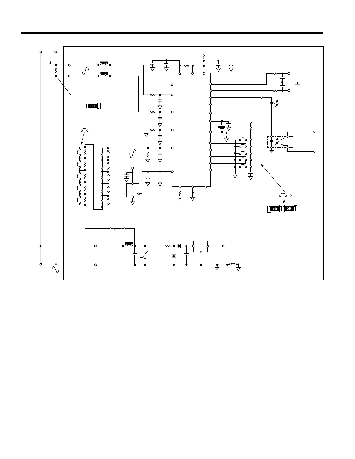
The schematic in Figure 1 shows the implementation of
a simple, low-cost watt-hour meter using the AD7755. A
shunt is used to provide the current-to-voltage conversion needed by the AD7755 and a simple divider
network attenuates the line voltage. The energy register
(kWh) is a simple electromechanical counter that uses a
two-phase stepper motor. The AD7755 provides direct
drive capability for this type of counter. The AD7755 also
provides a high-frequency output at the CF pin for the
meter constant (3200 imp/kWh). Thus a high-frequency
output is available at the LED and opto-isolator output.
This high-frequency output is used to speed up the
calibration process and provides a means of quickly
verifying meter functionality and accuracy in a production
environment. The meter is calibrated by varying the line
voltage attenuation using the resistor network R5 to R14.
Table I. Accuracy Requirements
3
1
MAX
Percentage Error Limits
Class 1 Class 2
PF
2
1 ±1.0% ±2.0%
0.8 Lead ±1.5%
MAX
0.5 Lag ±1.0% ±2.0%
0.8 Lead ±1.0%
Energy
=×
Registered by Meter – True Energy
True Energy
100%
REV. A
Page 2
AN-559
NEUTRAL
LOAD
PHASE
V
U1
REVP
NC
CLKOUT
CLKIN
SCF
DGND
POWER SUPPLY
8
U2
7805
2,3,6,7
DD
C12
C13
P1
P24
F1
P23
F2
P22
CF
P20
P19
P18
Y1
P17
G0
P16
G1
P15
S0
P14
S1
P13
P12
NC = NO CONNECT
V
DD
1
5V
+
V
C9
C8
Z2
DD
R17
J15
J14
J13
J12
J11
C7
TO IMPULSE COUNTER/
STEPPER MOTOR
R20
R19
R18
CALIBRATION
D1
LED
1
2
U3
PS2501-1
JUMPERS USE
0 RESISTOR
C15
C14
4
3
K5
K6
100 imp/kWhr
K7
3200 imp/kWhr
K8
CALIBRATION
NETWORK
R9
R14
R8
R13
R7
R12
R6
R11
R5
R10
K3
K4
Z3
Z4
J10
J9
C19
J8
J7
J6
R15 R16
AD780
Z1
C16
V
U4
4
K1
–
350
+
K2
JUMPERS USE
0 RESISTOR
J5
J4
J3
J2
J1
DD
2
6
+
C11
R1
R2
R3
R4
+
C5 C6
EXTERNAL
REFERENCE
(OPTIONAL)
C17
MOV1
C10
P3 P2
AVDD AC/DC DVDD
P4
NC
P5
V1P
C1
P6
V1N
C2
P7
V2N
C3
P8
V2P
C4
P10
REF
IN/OUT
RESET
P9 P11 P21
R23
V
DD
R21 D2
D3
C18
R22
AD7755
AGND
+
220V
Figure 1. Simple Single-Phase Watt-Hour Meter Based on the AD7755
DESIGN EQUATIONS
The AD7755 produces an output frequency that is proportional to the time average value of the product of two
voltage signals. The input voltage signals are applied at
V1 and V2. The detailed functionality of the AD7755 is
explained in the AD7755 data sheet, Theory Of Operation section. The AD7755 data sheet also provides an
equation that relates the output frequency on F1 and F2
(counter drive) to the product of the rms signal levels
at V1 and V2. This equation is shown here again for
convenience and will be used to determine the correct
signal scaling at V2 in order to calibrate the meter to a
fixed constant.
Frequency
=
×× × ×8.06 1
2
2
V
REF
1–4
(1)
V V Gain F
The meter shown in Figure 1 is designed to operate at
a line voltage of 220 V and a maximum current (I
MAX
) of
40 A. However, by correctly scaling the signals on
Channel 1 and Channel 2, a meter operating of any line
voltage and maximum current could be designed.
The four frequency options available on the AD7755 will
allow similar meters (i.e., direct counter drive) with an
I
of up to 120 A to be designed. The basic current (Ib)
MAX
for this meter is selected as 5 A and the current range for
accuracy will be 2% Ib to I
, or a dynamic range of 400
MAX
(100 mA to 40 A). The electromechanical register (kWh)
will have a constant of 100 imp/kWh, i.e., 100 impulses
from the AD7755 will be required in order to register
1 kWh. IEC1036 section 4.2.11 specifies that electromagnetic registers have their lowest values numbered in ten
division, each division being subdivided into ten parts.
Hence a display with a five plus one digits is used, i.e.,
10,000s, 1,000s, 100s, 10s, 1s, 1/10s. The meter constant
(for calibration and test) is selected as 3200 imp/kWh.
–2–
REV. A
Page 3
AN-559
Design Calculations
Design parameters:
Line voltage = 220 V (nominal)
I
= 40 A (Ib = 5 A)
MAX
Counter = 100 imp/kWh
Meter constant = 3200 imp/kWh
Shunt size = 350 µΩ
100 imp/hour = 100/3600 sec = 0.027777 Hz
Meter will be calibrated at Ib (5A)
Power dissipation at Ib = 220 V × 5 A = 1.1 kW
Frequency on F1 (and F2) at Ib = 1.1 × 0.027777 Hz
= 0.0305555 Hz
Voltage across shunt (V1) at Ib = 5 A × 350 µΩ = 1.75 mV.
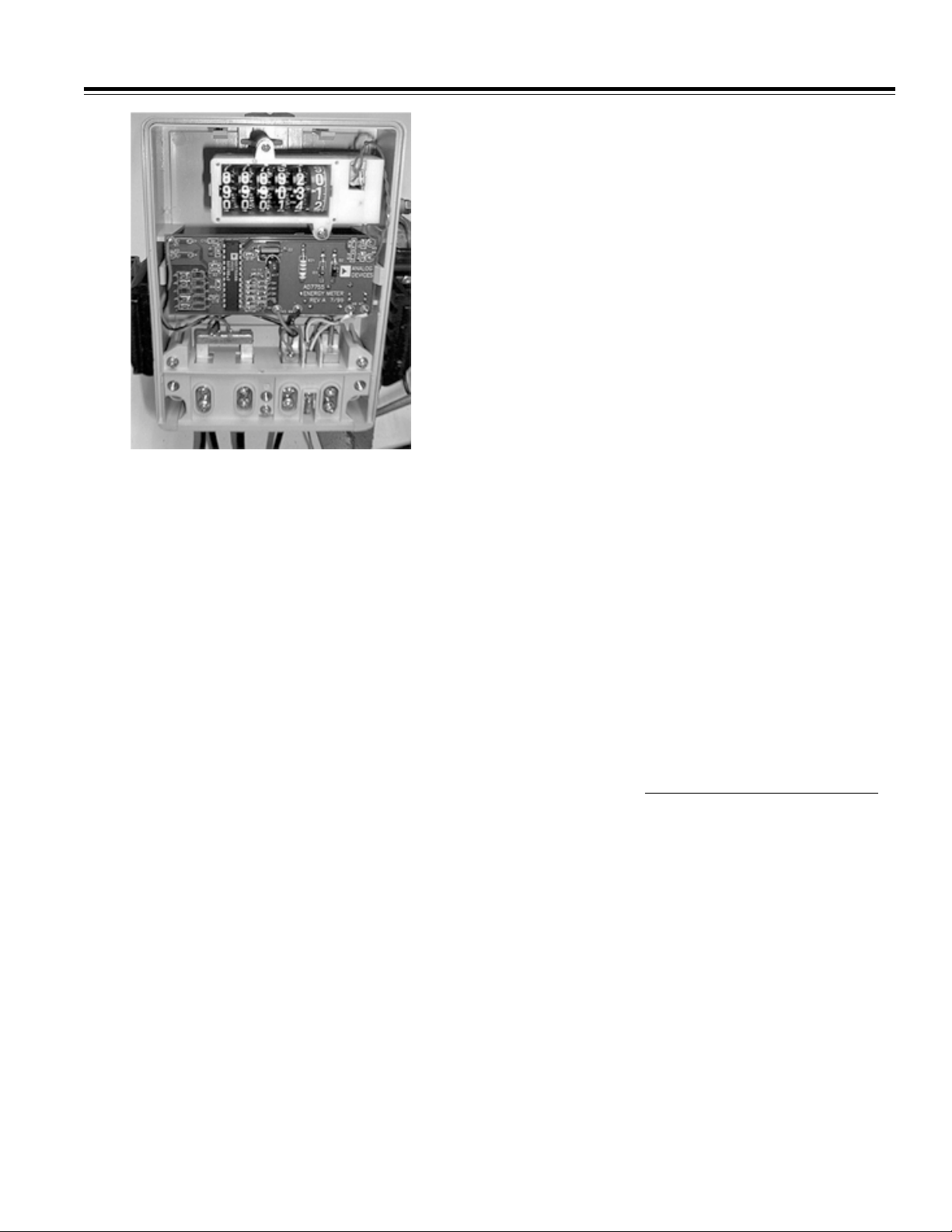
Figure 2. Final Implementation of the AD7755 Meter
AD7755 Reference
The schematic in Figure 1 also shows an optional reference
circuit. The on-chip reference circuit of the AD7755 has a
temperature coefficient of typically 30 ppm/°C. However,
on A Grade parts this specification is not guaranteed
and may be as high as 80 ppm/°C. At 80 ppm/°C the
AD7755 error at –20°C/+60°C could be as high as 0.65%,
assuming a calibration at 25°C.
Shunt Selection
The shunt size (350 µΩ) is selected to maximize the use
of the dynamic range on Channel V1 (current channel).
However there are some important considerations when
selecting a shunt for an energy metering application.
First, minimize the power dissipation in the shunt. The
maximum rated current for this design is 40 A, therefore,
the maximum power dissipated in the shunt is (40 A)
350 µΩ = 560 mW. IEC1036 calls for a maximum power
dissipation of 2 W (including power supply). Secondly,
the higher power dissipation may make it difficult to
manage the thermal issues. Although the shunt is
manufactured from Manganin material, which is an
alloy with a low temperature coefficient of resistance,
high temperatures may cause significant error at heavy
loads. A third consideration is the ability of the meter to
resist attempts to tamper by shorting the phase circuit.
With a very low value of shunt resistance the effects of
externally shorting the shunt are very much minimized.
Therefore, the shunt should always be made as small as
possible, but this must be offset against the signal range
on V1 (0 mV–20 mV rms with a gain of 16). If the shunt is
made too small it will not be possible to meet the
IEC1036 accuracy requirements at light loads. A shunt
value of 350 µΩ was considered a good compromise for
this design.
2
×
To select the F
data sheet, Selecting a Frequency for an Energy Meter
Application section. From Tables V and VI in the AD7755
data sheet it can be seen that the best choice of frequency for a meter with I
frequency selection is made by the logic inputs S0 and
S1—see Table II in the AD7755 data sheet. The CF frequency selection (meter constant) is selected by using
the logic input SCF. The two available options are 64
F1(6400 imp/kWh) or 32 × F1(3200 imp/kWh). For this
design, 3200 imp/kWh is selected by setting SCF logic
low. With a meter constant of 3200 imp/kWh and a
maximum current of 40 A, the maximum frequency
from CF is 7.82 Hz. Many calibration benches used to
verify meter accuracy still use optical techniques. This
limits the maximum frequency that can be reliably read
to about 10 Hz. The only remaining unknown from
equation 1 is V2 or the signal level on Channel 2 (the
voltage channel).
From Equation 1 on the previous page:
0 030555
.
Therefore, in order to calibrate the meter the line voltage needs to be attenuated down to 248.9 mV.
CALIBRATING THE METER
From the previous section it can be seen that the meter
is simply calibrated by attenuating the line voltage down
to 248.9 mV. The line voltage attenuation is carried out
by a simple resistor divider as shown in Figure 3. The
attenuation network should allow a calibration range of
at least ±30% to allow for shunt tolerances and the on-chip
reference tolerance of ±8%—see AD7755 data sheet.
In addition, the topology of the network is such that the
phase-matching between Channel 1 and Channel 2 is
preserved, even when the attenuation is being adjusted
(see Correct Phase Matching Between Channels section).
frequency for Equation 1 see the AD7755
1–4
= 40 A is 3.4 Hz (F2). This
MAX
8 06 1 75 2 16 3 4
Hz
.. .
=
V2 = 248.9 mV rms
mV V Hz
××××
25
.
2
REV. A
–3–
Page 4
AN-559
248.9mV
R9
J5
J4
J3
J2
J1
R14
R8
R13
R7
R12
R6
R11
R5
R10
J10
J9
J8
J7
J6
R15 R16
R4 C4
R5 + R6 + ............. + R15 + R16 >> R4
1/(2..R4.C4)
f
–3dB
220V
Figure 3. Attenuation Network
As can be seen from Figure 3, the –3 dB frequency of this
network is determined by R4 and C4. Even with all the
jumpers closed, the resistance of R15 (330 kΩ) and R16
(330 kΩ) is still much greater than R4 (1 kΩ). Hence varying the resistance of the resistor chain R5 to R14 will
have little effect on the –3 dB frequency of the network.
The network shown in Figure 3 allows the line voltage
to be attenuated and adjusted in the range 175 mV to
333 mV with a resolution of 10 bits or 154 µV. This is
achieved by using the binary weighted resistor chain R5
to R14. This will allow the meter to be accurately calibrated using a successive approximation technique.
Starting with J1, each jumper is closed in order of
ascendance, e.g., J1, J2, J3, etc. If the calibration frequency on CF, i.e., 32 × 100 imp/hr (0.9777 Hz), is
exceeded when any jumper is closed, it should be
opened again. All jumpers are tested, J10 being the last
jumper. Note jumper connections are made with 0 Ω
fixed resistors which are soldered into place. This approach
is preferred over the use of trim pots, as the stability of
the latter over time and environmental conditions is
questionable.
Since the AD7755 transfer function is extremely linear a
one-point calibration (Ib) at unity power factor, is all that
is needed to calibrate the meter. If the correct precautions have been taken at the design stage, no calibration
will be necessary at low-power factor (PF = 0.5). The
next section discusses phase matching for correct calculation of energy at low-power factor.
If, however, a phase error (φ
) is introduced externally to
e
the AD7755, e.g., in the antialias filters, the error is calculated as:
[cos(δ°) – cos(δ°+ φ
)]/cos(δ°) × 100% (2)
e
See Note 3 on Table I. Where δ is the phase angle between
voltage and current and φ
is the external phase error.
e
With a phase error of 0.2°, for example, the error at
PF = 0.5 (60°) is calculated as 0.6%. As this example
demonstrates, even a very small phase error will produce a large measurement error at low power factor.
PF = 1
V.I
PF = 0.5
V.I COS(60)
2
2
CURRENT
VOLTAGE
VOLTAGE
CURRENT
INSTANTANEOUS
POWER SIGNAL
INSTANTANEOUS
POWER SIGNAL
60
INSTANTANEOUS REAL
POWER SIGNAL
INSTANTANEOUS REAL
POWER SIGNAL
Figure 4. Voltage and Current (Inductive Load)
ANTIALIAS FILTERS
As mentioned in the previous section, one possible
source of external phase errors are the antialias filters
on Channel 1 and Channel 2. The antialias filters are lowpass filters that are placed before the analog inputs of any
ADC. They are required to prevent a possible distortion
due to sampling called aliasing. Figure 5 illustrates the
effects of aliasing.
CORRECT PHASE MATCHING BETWEEN CHANNELS
The AD7755 is internally phase-matched over the frequency range 40 Hz to 1 kHz. Correct phase matching is
important in an energy metering application because
any phase mismatch between channels will translate
into significant measurement error at low-power factor. This is easily illustrated with the following example.
Figure 4 shows the voltage and current waveforms for
an inductive load. In the example shown, the current
lags the voltage by 60° (PF = –0.5). Assuming pure sinusoidal conditions, the power is easily calculated as
V rms × I rms × cos (60°).
–4–
0
IMAGE
FREQUENCIES
2
Figure 5. Aliasing Effects
450
FREQUENCY – kHz
900
REV. A
Page 5
AN-559
Figure 5 shows how aliasing effects could introduce inaccuracies in an AD7755-based meter design. The AD7755
uses two Σ-∆ ADCs to digitize the voltage and current
signals. These ADCs have a very high sampling rate, i.e.,
900 kHz. Figure 5 shows how frequency components
(arrows shown in black) above half the sampling frequency (also know as the Nyquist frequency), i.e., 450 kHz
is imaged or folded back down below 450 kHz (arrows
shown dashed). This will happen with all ADCs no matter what the architecture. In the example shown it can be
seen that only frequencies near the sampling frequency,
i.e., 900 kHz, will move into the band of interest for metering, i.e., 0 kHz–2 kHz. This fact will allow us to use a very
simple LPF (Low-Pass Filter) to attenuate these high frequencies (near 900 kHz) and so prevent distortion in the
band of interest.
The simplest form of LPF is the simple RC filter. This is
a single-pole filter with a roll-off or attenuation of
–20 dBs/dec.
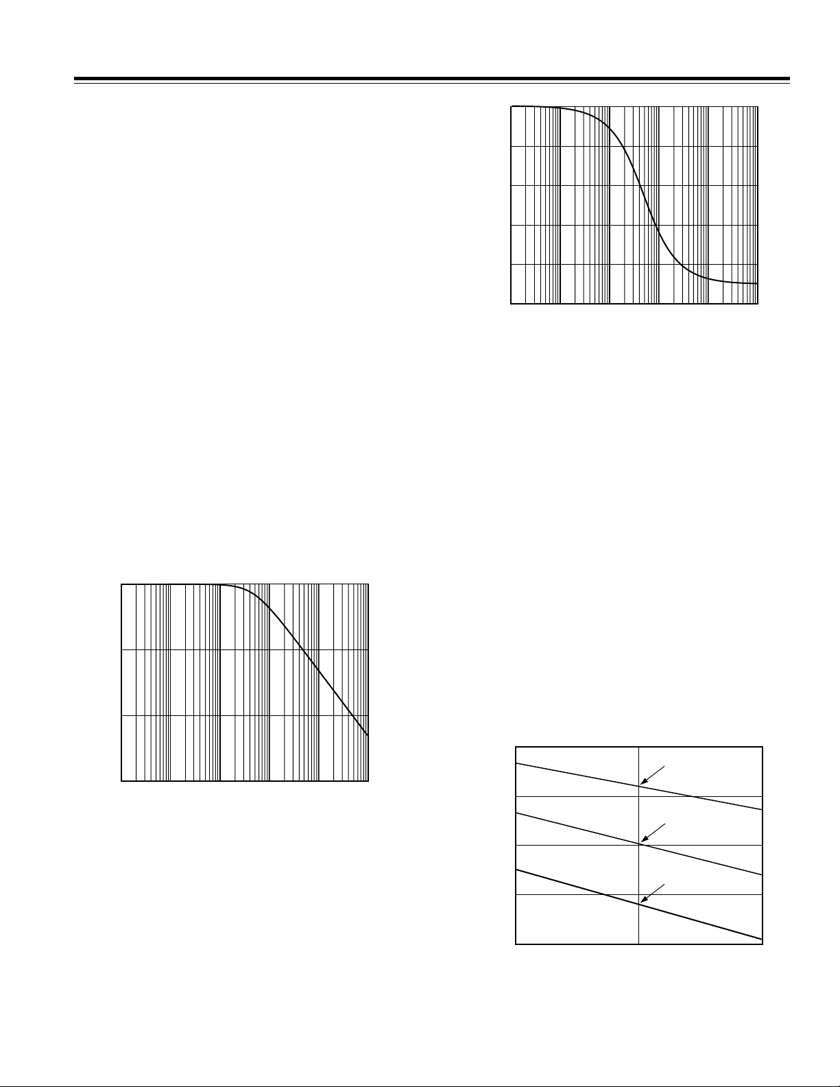
Choosing the Filter –3 dB Frequency
As well as having a magnitude response, all filters also
have a phase response. The magnitude and phase
response of a simple RC filter (R = 1 kΩ, C = 33 nF) are
shown in Figures 6 and 7. From Figure 6 it is seen that
the attenuation at 900 kHz for this simple LPF is greater
than 40 dBs. This is enough attenuation to ensure no ill
effects due to aliasing.
0
–20
dB
–40
0
–20
–40
DEGREES
–60
–80
–100
1k10010
FREQUENCY – Hz
10k
100k 1M
Figure 7. RC Filter Phase Response
As explained in the last section, the phase response can
introduce significant errors if the phase response of the
LPFs on both Channel 1 and Channel 2 are not matched.
Phase mismatch can easily occur due to poor component
tolerances in the LPF. The lower the –3 dB frequency in the
LPF (antialias filter) the more pronounced these errors
will be at the fundamental frequency component or the
line frequency. Even with the corner frequency set at
4.8 kHz (R = 1 kΩ, C = 33 nF) the phase errors due to poor
component tolerances can be significant. Figure 8 illustrates the point. In Figure 8, the phase response for the
simple LPF is shown at 50 Hz for R = 1 kΩ ± 10%, C = 33 nF
± 10%. Remember a phase shift of 0.2° can causes measurement errors of 0.6% at low-power factor. This
design uses resistors of 1% tolerance and capacitors of
10% tolerance for the antialias filters to reduce the possible problems due to phase mismatch. Alternatively the
corner frequency of the antialias filter could be pushed
out to 10 kHz–15 Hz. However, the corner frequency
should not be made too high, as this could allow enough
high-frequency components to be aliased and so cause
accuracy problems in a noisy environment.
REV. A
–60
1k10010
FREQUENCY – Hz
10k
100k 1M
Figure 6. RC Filter Magnitude Response
–5–
–0.4
–0.5
–0.6
DEGREES
–0.7
–0.8
45
FREQUENCY – Hz
(50Hz, –0.481)
(R = 900, C = 29.7nF)
(50Hz, –0.594)
(R = 1k, C = 33nF)
(50Hz, –0.718)
(R = 1.1k, C = 36.3nF)
50
55
Figure 8. Phase Shift at 50 Hz Due to Component
Tolerances
Page 6
AN-559
L
SH2
L
GND
R
GND
GND
R
SH2
R
SH1
L
SH1
L
W2
R2
R1
L
W1
V1N
V1P
C2
C1
IN
OUT
PHASE
V1N
V1P
SHUNT 330
GND
FREQUENCY – Hz
10
–100
10k
100k 1M
1k
100
–50dB
–40dB
–30dB
–20dB
–10dB
0dB
–80
–60
–40
–20
–0
PHASE
MAGNITUDE
Note that this is also why precautions were taken with
the design of the calibration network on Channel 2 (voltage channel). Calibrating the meter by varying the
resistance of the attenuation network will not vary the
–3 dB frequency and hence the phase response of the
network on Channel 2—see Calibrating the Meter section. Shown in Figure 9 is a plot of phase lag at 50 Hz
when the resistance of the calibration network is varied
from 660 kΩ (J1–J10 closed) to 1.26 MΩ (J1–J10 open).
–0.591
–0.592
–0.593
DEGREES
–0.594
–0.595
J1–J10 OPEN
(50Hz, –0.59348)
49.9 50.0
FREQUENCY – Hz
Figure 9. Phase Shift Due to Calibration
COMPENSATING FOR PARASITIC SHUNT INDUCTANCE
When used at low frequencies a shunt can be considered a
purely resistive element with no significant reactive elements. However, under certain situations even a small
amount of stray inductance can cause undesirable effects
when a shunt is used in a practical data acquisition system. The problem is very noticeable when the resistance
of the shunt is very low, in the order of 200 µΩ. Shown
below is an equivalent circuit for the shunt used in the
AD7755 reference design. There are three connections
to the shunt. One pair of connections provides the current sense inputs (V1P and V1N) and the third connection
is the ground reference for the system.
J1–J10 CLOSED
(50Hz, –0.59308)
50.1
Figure 10. Equivalent Circuit for the Shunt
Canceling the Effects of the Parasitic Shunt Inductance
The effect of the parasitic shunt inductance is shown in
Figure 11. The plot shows the phase and magnitude
response of the antialias filter network with and without
(dashed) a parasitic inductance of 2 nH. As can be seen
from the plot, both the gain and phase response of the
network are affected. The attenuation at 1 MHz is now
only about –15 dB, which could cause some repeatability and accuracy problems in a noisy environment. More
importantly, a phase mismatch may now exist between
the current and voltage channels. Assuming the network
on Channel 2 has been designed to match the ideal
phase response of Channel 1, there now exists a phase
mismatch of 0.1° at 50 Hz. Note that 0.1° will cause a
0.3% measurement error at PF = ±0.5. See Equation 2
(Correct Phase Matching Between Channels).
The shunt resistance is shown as R
(350 µΩ). R
SH1
the resistance between the V1N input terminal and the
system ground reference point. The main parasitic elements (inductance) are shown as L
SH1
and L
10 also shows how the shunt is connected to the AD7755
inputs (V1P and V1N) through the antialias filters. The
function of the antialias filters is explained in the previous section and their ideal magnitude and phase
responses are shown in Figures 6 and 7.
. Figure
SH2
SH2
is
Figure 11. Effect of Parasitic Shunt Inductance on the
Antialias Network
The problem is caused by the addition of a zero into the
antialias network. Using the simple model for the shunt
shown in Figure 10, the location of the zero is given as
R
SH1/LSH1
radians.
One way to cancel the effects of this additional zero in
the network is to add an additional pole at (or close to)
the same location. The addition of an extra RC on each
analog input of Channel 1 will achieve the additional
–6–
REV. A
Page 7
AN-559
FREQUENCY – Hz
10
–100
10k 100k 1M
1k
100
–50dB
–40dB
–30dB
–20dB
–10dB
0dB
–80
–60
–40
–20
–0
MAGNITUDE
PHASE
pole required. The new antialias network for Channel 1
is shown in Figure 12. To simplify the calculation and
demonstrate the principle, the Rs and Cs of the network
are assumed to have the same value.
j
POLE #1
POLE #2
3
2
RR
5
11
–
RC
4
RC
C
H (s) =
3
11
–
2
RC
ZERO #1
–(RSH/LSH)
2R2C2
S
+ S3RC + 1
+
1
5
4
RC
–
C
Figure 12. Shunt Inductance Compensation Network
Figure 12 also gives an expression for the location of the
poles of this compensation network. The purpose of
Pole #1 is to cancel the effects of the zero due to the
shunt inductance. Pole #2 will perform the function of
the antialias filters as described in the Antialias Filters
section. The following illustrates a sample calculation
for a shunt of 330 µΩ with a parasitic inductance of 2 nH.
The location of the pole #1 is given as:
321541
−× + ×
RC
For
R
= 330 µΩ,
SH
1
R
is calculated as approximately 480 Ω (use 470 Ω).
L
SH
= 2 nH,
1
RC
C
= 33 nF
R
1
SH
=
L
1
SH
The location of Pole #1 is 165,000 rads or 26.26 kHz.
This places the location of Pole # 2 at:
321
−× + ×
RC541RC
=
3.838 kHz
To ensure phase-matching between Channel 1 and
Channel 2, the pole at Channel 2 must also be positioned
at this location. With C = 33 nF, the new value of resistance
for the antialias filters on Channel 2 is approximately
1.23 kΩ (use 1.2 kΩ).
Figure 13 shows the effect of the compensation network
on the phase and magnitude response of the antialias
network in Channel 1. The dashed line shows the
response of Channel 2 using practical values for the
newly calculated component values, i.e., 1.2 kΩ and
33 nF. The solid line shows the response of Channel 1
with the parasitic shunt inductance included. Notice
phase and magnitude responses match very closely
with the ideal response—shown as a dashed line. This is
the objective of the compensation network.
Figure 13. Antialias Network Phase and Magnitude
Response after Compensation
The method of compensation works well when the pole
due to shunt inductance is less than 25 kHz or so. If zero
is at a much higher frequency its effects may simply be
eliminated by placing an extra RC on Channel 1 with a
pole that is a decade greater than that of the antialias
filter, e.g., 100 Ω and 33 nF.
Care should be taken when selecting a shunt to ensure
its parasitic inductance is small. This is especially true of
shunts with small values of resistance, e.g., <200 µΩ. Note
that the smaller the shunt resistance, the lower the
zero frequency for a given parasitic inductance (Zero =
R
SH1/LSH1
).
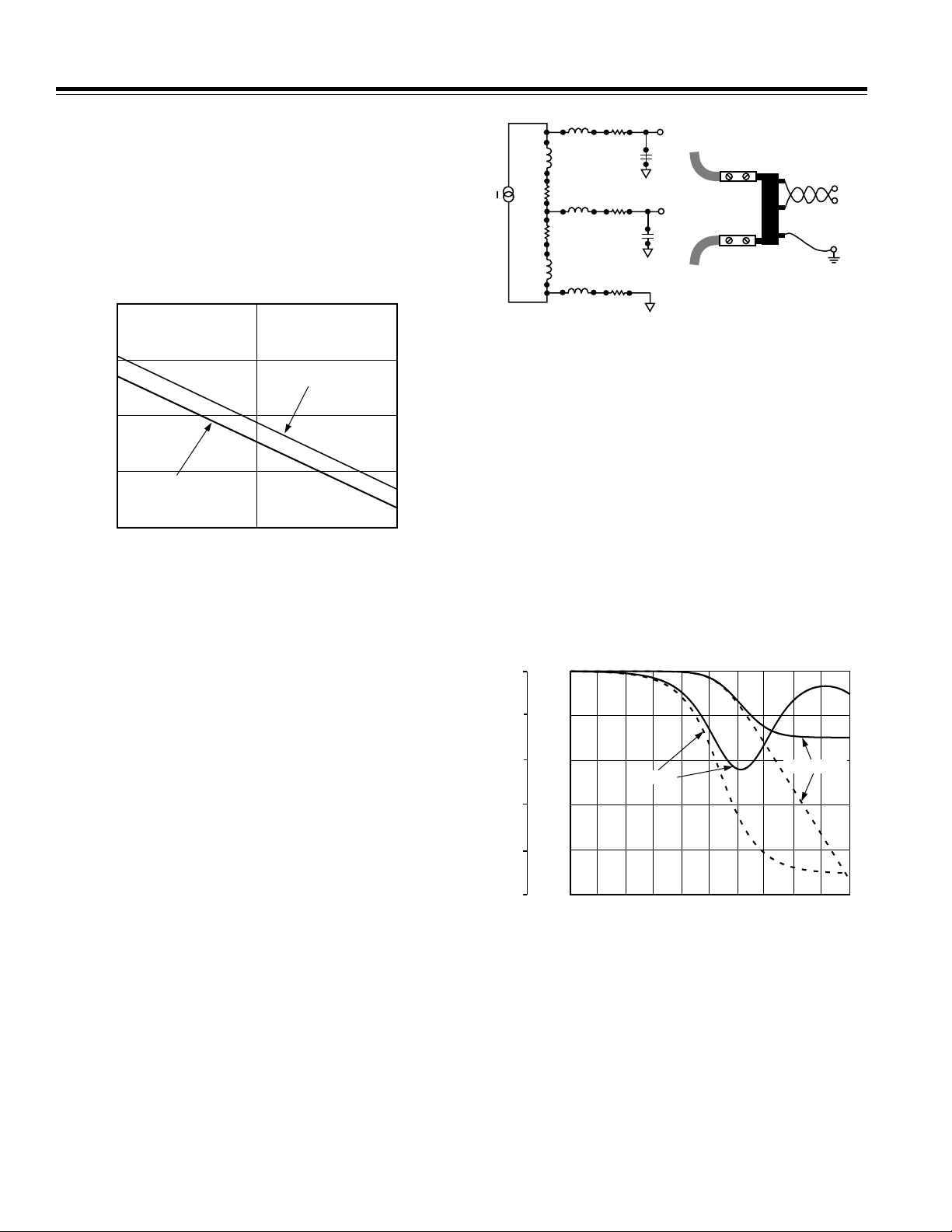
POWER SUPPLY DESIGN
This design uses a simple low-cost power supply based
on a capacitor divider network, i.e., C17 and C18. Most of
the line voltage is dropped across C17, a 470 nF 250 V
metalized polyester film capacitor. The impedance of
C17 dictates the effective VA rating of the supply. However the size of C17 is constrained by the power
consumption specification in IEC1036. The total power
consumption in the voltage circuit, including power supply, is specified in section 4.4.1.1 of IEC1036 (1996-9).
The total power consumption in each phase is 2 W and
10 VA under nominal conditions. The nominal VA rating of
the supply in this design is 7 VA. The total power dissipation is approximately 0.5 W. Together with the power
dissipated in the shunt at 40 A load, the total power consumption of the meter is 1.06 W. Figure 14 shows the
basic power supply design.
REV. A
–7–
Page 8

AN-559
220V
C17
R21
V1
D2
+
C18
D3
U2
7805
5V
V2
V
D
Figure 14. Power Supply
The plots shown in Figures 15, 16, 17, and 18 show the
PSU performance under heavy load (50 A) with the line
voltage varied from 180 V to 250 V. By far the biggest
load on the power supply is the current required to drive
the stepper motor which has a coil impedance of about
400 Ω. This is clearly seen by looking at V1 (voltage on
C18) in the plots below. Figure 16 shows the current
drawn from the supply. Refer to Figure 14 when reviewing the simulation plots below.
15
10
VOLTS
5
V1
(C18)
V2
(V
DD
C18 VOLTAGE DROP DUE TO
)
STEPPER MOTOR DRIVE
15
10
V2
)
VOLTS
5
0
0102
V1
(C18)
(V
DD
468
TIME – s
Figure 17. Power Supply Voltage Output at 180 V and
50 A Load
15
10
V1
(C18)
VOLTS
5
V2
(V
)
DD
0
0
2
4
68
TIME – s
10
Figure 15. Power Supply Voltage Output at 220 V and
50 A Load
24
12.5mA
MOTOR DRIVE
20
16
4 mA LED/OPTO DRIVE
12
mA
8
4
0
0
234
TIME – s
51
Figure 16. Power Supply Current Output at 220 V and
50 A Load
0
0102
468
TIME – s
Figure 18. Power Supply Voltage Output at 250 V and
50 A Load
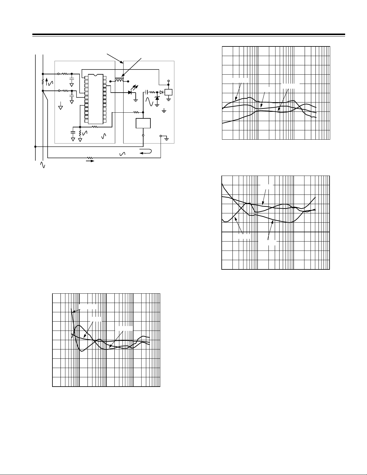
DESIGN FOR IMMUNITY TO ELECTROMAGNETIC
DISTURBANCE
In Section 4.5 of IEC1036 it is stated that “the meter shall
be designed in such a way that conducted or radiated
electromagnetic disturbances as well as electrostatic discharge do not damage nor substantially influence the
meter.” The considered disturbances are:
1. Electrostatic Discharge
2. Electromagnetic HF Fields
3. Fast Transience Burst
All of the precautions and design techniques (e.g., ferrite
beads, capacitor line filters, physically large SMD resistors, PCB layout including grounding) contribute to a
certain extent in protecting the meter electronics from
each form of electromagnetic disturbance. Some precautions (e.g., ferrite beads), however, play a more important
role in the presence of certain kinds of disturbances
(e.g., RF and fast transience burst). The following discuses each of the disturbances listed above and details
what protection has been put in place.
–8–
REV. A
Page 9

AN-559
TO EXTERIOR
(I/O) CONNECTION
8kV ESD
EVENT
6–9 MILS
NO SOLDER
MASK
TRACE (TRACK)
ESD DISCHARGED
ACROSS SPARK GAP
TO CIRCUIT
SIGNAL
GROUND
103
ELECTROSTATIC DISCHARGE (ESD)
Although many sensitive electronic components contain a certain amount of ESD protection on-chip, it is not
possible to protect against the kind of severe discharge
described below. Another problem is that the effect of
an ESD discharge is cumulative, i.e., a device may survive an ESD discharge, but it is no guarantee that it will
survive multiple discharges at some stage in the future.
The best approach is to eliminate or attenuate the
effects of the ESD event before it comes in contact
with sensitive electronic devices. This holds true for all
conducted electromagnetic disturbances. This test is
carried out according to IEC1000-4-2, under the following conditions:
– Contact Discharge;
– Test Severity Level 4;
– Test Voltage 8 kV;
– 10 Discharges.
Very often no additional components are necessary to
protect devices. With a little care those components
already required in the circuit can perform a dual role.
For example, the meter must be protected from ESD
events at those points where it comes in contact with the
“outside world,” e.g., the connection to the shunt. Here
the AD7755 is connected to the shunt via two LPFs (antialias filters) which are required by the ADC—see
Antialias Filters section. This RC filter can also be
enough to protect against ESD damage to CMOS
devices. However, some care must be taken with the
type of components used. For example, the resistors
should not be wire-wound as the discharge will simply
travel across them. The resistors should also be physically large to stop the discharge arcing across the
resistor. In this design 1/8W SMD 1206 resistors were
used in the antialias filters. Two ferrite beads are also
placed in series with the connection to the shunt. A ferrite
choke is particularly effective at slowing the fast rise
time of an ESD current pulse. The high-frequency transient energy is absorbed in the ferrite material rather than
being diverted or reflected to another part of the system.
(
The properties of ferrite are discussed later
.) The PSU circuit is also directly connected to the terminals of the
meter. Here the discharge will be dissipated by the ferrite, the line filter capacitor (C16), and the rectification
diodes D2 and D3. The analog input V2P is protected by
the large impedance of the attenuation network used
for calibration.
Another very common low-cost technique employed to
arrest ESD events is to use a spark gap on the component side of the PCB—see Figure 19. However, since the
meter will likely operate in an open air environment and
be subject to many discharges, this is not recommended
at sensitive nodes like the shunt connection. Multiple
REV. A
discharges could cause carbon buildup across the spark
gap which could cause a short or introduce an impedance that will in time affect accuracy. A spark gap was
introduced in the PSU after the MOV to take care of any
very high amplitude/fast rise time discharges.
Figure 19. Spark Gap to Arrest ESD Events
ELECTROMAGNETIC HF FIELDS
Testing is carried out according to IEC100-4-3. Susceptibility of integrated circuits to RF tends to be more
pronounced in the 20 MHz–200 MHz region. Frequencies
higher that this tend to be shunted away from sensitive
devices by parasitic capacitances. In general, at the IC
level, the effects of RF in the region 20 MHz–200 MHz
will tend to be broadband in nature, i.e., no individual
frequency is more troublesome than another. However,
there may be higher sensitivity to certain frequencies
due to resonances on the PCB. These resonances could
cause insertion gain at certain frequencies which, in
turn, could cause problems for sensitive devices. By far
the greatest RF signal levels are those coupled into
the system via cabling. These connection points should
be protected. Some techniques for protecting the system are:
1. Minimize Circuit Bandwidth
2. Isolate Sensitive Parts of the System
Minimize Bandwidth
In this application the required analog bandwidth is
only 2 kHz. This is a significant advantage when trying
to reduce the effects of RF. The cable entry points can be
low-pass filtered to reduce the amount of RF radiation
entering the system. The shunt output is already filtered
before being connected to the AD7755. This is to prevent
aliasing effects that were described earlier. By choosing
the correct components and adding some additional
components (e.g., ferrite beads) these antialias filters
can double as very effective RF filters. Figure 7 shows a
somewhat idealized frequency response for the antialias
filters on the analog inputs. When considering higher
frequencies (e.g., > 1 MHz), the parasitic reactive elements of each lumped component must be considered.
Figure 20 shows the antialias filters with the parasitic
elements included. These small values of parasitic capacitance and inductance become significant at higher
frequencies and therefore must be considered.
–9–
Page 10

AN-559
I/O
CONNECTION
"MOAT" – NO
POWER OR
GROUND PLANE
POWER CONNECTION
MADE USING FERRITE
"BEAD ON LEAD"
Z3
K1
LOW Z HIGH Z
K2
R1
C1
Z4
R2
C2
Figure 20. Antialias Filters Showing Parasitics
Parasitics can be kept at a minimum by using physically
small components with short lead lengths (i.e., surface
mount). Because the exact source impedance conditions
are not known (this will depend on the source impedance of the electricity supply), some general precautions
should be taken to minimize the effects of potential resonances. Resonances that result from the interaction of
the source impedance and filter networks could cause
insertion gain effects and so increase the exposure of
the system to RF radiation at certain (resonant) frequencies. Lossy (i.e., having large resistive elements)
components like capacitors with lossy dielectric (e.g.,
Type X7R) and ferrite are ideal components for reducing
the “Q” of the input network. The RF radiation is dissipated as heat, rather than being reflected or diverted to
another part of the system. The ferrite beads Z3 and Z4
perform very well in this respect. Figure 21 shows how the
impedance of the ferrite beads varies with frequency.
250
LI 1806 B 151R
Z, R, X
VS. FREQUENCY
L
FREQUENCY – MHz
Z
R
X
L
10010
200
150
100
50
0
1 1000
Figure 21. Frequency Response of the Ferrite Chips
(Z3 and Z4) in the Antialias Filter
From Figure 21 it can be seen that the ferrite material
becomes predominately resistive at high frequencies.
Note also that the impedance of the ferrite material
V1P
V1N
increases with frequency, causing only high (RF) frequencies to be attenuated.
Isolation
The shunt connection is the only location where the
AD7755 is connected directly (via antialias filters) to the
“outside world.” The system is also connected to the
phase and neutral lines for the purpose of generating a
power supply and voltage channel signal (V2). The ferrite
bead (Z1) and line filter capacitor (C16) should significantly reduce any RF radiation on the power supply.
Another possible path for RF is the signal ground for the
system. A moating technique has been used to help isolate the signal ground surrounding the AD7755 from the
external ground reference point (K4). Figure 22 illustrates the principle of this technique called partitioning
or “moating.”
Figure 22. High-Frequency Isolation of I/O Connections
Using a “Moat”
Sensitive regions of the system are protected from RF
radiation entering the system at the I/O connection. An
area surrounding the I/O connection does not have any
ground or power planes. This limits the conduction
paths for RF radiation and is called a “moat.” Obviously
power, ground, and signal connections must cross this
moat and Figure 22 shows how this can be safely
achieved by using a ferrite bead. Remember that ferrite offers a large impedance to high frequencies (see
Figure 21).
ELECTRICAL FAST TRANSIENCE (EFT) BURST TESTING
This testing determines the immunity of a system to
conducted transients. Testing is carried out in accordance
with IEC1000-4-4 under well-defined conditions. The EFT
pulse can be particularly difficult to guard against because
the disturbance is conducted into the system via external connections, e.g., power lines. Figure 23 shows the
physical properties of the EFT pulse used in IEC1000-4-4.
Perhaps the most debilitating attribute of the pulse is
not its amplitude (which can be as high as 4 kV), but
–10–
REV. A
Page 11
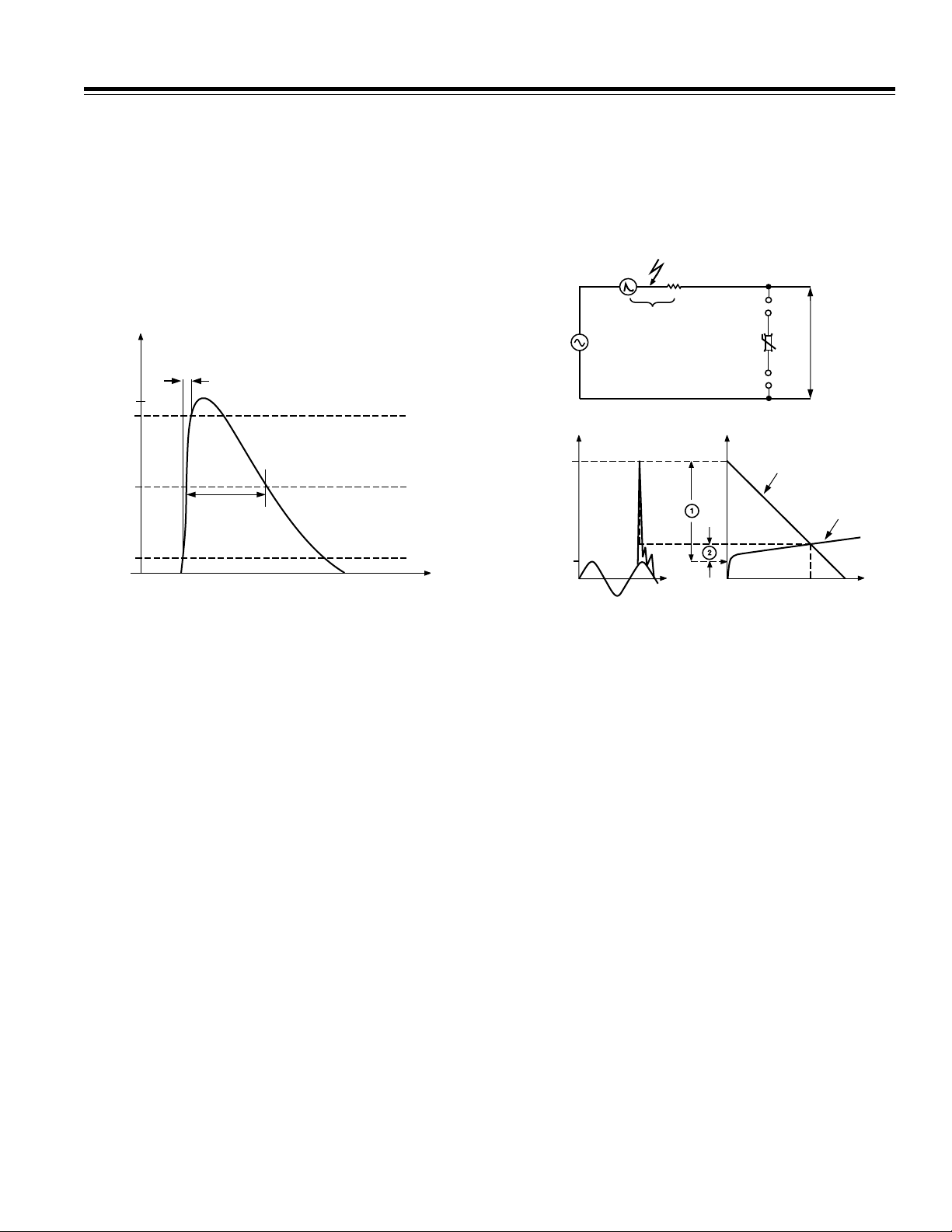
AN-559
t
VB, V
MOV
i*
i*
i
LEAKAGE
CURRENT >> 0
SURGE
CURRENT
V/I CHARACTERITIC
CURVE OF MOV
"LOAD LINE" OF
THE OVERVOLTAGE
V
V
V
S
V
B
V
S
Z
S
MOV
ELECTRONIC
CIRCUIT
TO BE
PROTECTED
TAKEN FROM SIEMENS MATSUSHITA COMPONENTS
SIOV METAL OXIDE VARISTOR CATALOG
*
OVERVOLTAGE
SOURCE
the high-frequency content due to the fast rise times
involved. Fast rise times mean high-frequency content
which allows the pulse to couple to other parts of the
system through stray capacitance, etc. Large differential
signals can be generated by the inductance of PCB
traces and signal ground. These large differential signals could interrupt the operation of sensitive
electronic components. Digital systems are generally
most at risk because of data corruption. Analog electronic systems tend only to be affected for the duration
of the disturbance.
5ns
4kV
90%
50%
50ns
10%
device or circuit being protected. During an overvoltage
event they form a low-resistance shunt and thus prevent
any further rise in the voltage across the circuit being
protected. The overvoltage is essentially dropped
across the source impedance of the overvoltage source,
e.g., the mains network source impedance. Figure 24
illustrates the principle of operation.
Figure 23. Single EFT Pulse Characteristics
Another possible issue with conducted EFT is that the
effects of the radiation will, like ESD, generally be cumulative for electronic components. The energy in an EFT
pulse can be as high as 4 mJ and deliver 40 A into a 50 Ω
load (see Figure 26). Therefore continued exposure to
EFT due to inductive load switching etc., may have implications for the long-term reliability of components. The
best approach is to protect those parts of the system
that could be sensitive to EFT.
The protection techniques described in the last section
(Electromagnetic HF Fields) also apply equally well in
the case of EFT. The electronics should be isolated as
much as possible from the source of the disturbance
through PCB layout (i.e., moating) and filtering signal
and power connections. In addition, a 10 nF capacitor
(C16) placed across the mains provides a low impedance shunt for differential EFT pulses. Stray inductance
due to leads and PCB traces will mean that the MOV
will not be very effective in attenuating the differential
EFT pulse. The MOV is very effective in attenuating high
energy, relatively long duration disturbances, e.g., due
to lighting strikes, etc. The MOV is discussed in the
next section.
MOV Type S20K275
The MOV used in this design was of type S20K275
from Siemens. An MOV is basically a voltage-dependant
resistor whose resistance decreases with increasing
voltage. They are typically connected in parallel with the
REV. A
TIME
Figure 24. Principle of MOV Overvoltage Protection
The plot in Figure 24 shows how the MOV voltage and
current can be estimated for a given overvoltage and
source impedance. A load line (open-circuit voltage,
short-circuit current) is plotted on the same graph as the
MOV characteristic curve. Where the curves intersect,
the MOV clamping voltage and current can be read.
Note that care must be taken when determining the
short-circuit current. The frequency content of the overvoltage must be taken into account as the source
impedance (e.g., mains) may vary considerably with frequency. A typical impedance of 50 Ω is used for mains
source impedance during fast transience (high-frequency)
pulse testing. The next section discusses IEC1000-4-4
and IEC1000-4-5, which are transience and overvoltage
EMC compliance tests.
IEC1000-4-4 and the S20K275
While the graphical technique just described is useful, an
even better approach is to use simulation to obtain a better
understanding of MOV operation. EPCOS Components
provides SPICE models for all their MOVs and these are
very useful in determining device operation under the
various IEC EMC compliance tests. For more information on EPCOS SPICE models and their applications see:
http://www.epcos.de/inf/70/e0000000.htm
–11–
Page 12

AN-559
The purpose of IEC1000-4-4 is to determine the effect of
repetitive, low energy, high-voltage, fast rise time pulses
on an electronic system. This test is intended to simulate
transient disturbances such as those originating from
switching transience (e.g., interruption of inductive loads,
relay contact bounce, etc.).
Figure 25 shows an equivalent circuit intended to replicate the EFT test pulse as specified in IEC1000-4-4. The
generator circuit is based on Figure 1 IEC1000-4-4 (1995-
01). The characteristics of operation are:
– Maximum energy of 4 mJ/pulse at 2 kV into 50 Ω
– Source impedance of 50 Ω ± 20%
– DC blocking capacitor of 10 nF
– Pulse rise time of 5 ns ± 30%
– Pulse duration (50% value) of 50 ns ± 30%
– Pulse shape as shown in Figure 23.
SW1 SW2
+
0.5kV
TO 5kV
C1
6F
R2
50
R1
0.01
C2
10nF
L1
5nH
C16
10nF
MOV
50
Figure 27 shows the generator output into 50 Ω load
with the MOV and some inductance (5 nH). This is
included to take into account stray inductance due to
PCB traces and leads. Although the simulation result
shows that the EFT pulse has been attenuated (600 V)
and most of the energy being absorbed by the MOV
(only 0.8 mJ is delivered to the 50 Ω load) it should be
noted that stray inductance and capacitance could render the MOV unless. For example Figure 28 shows the
same simulation with the stay inductance increased to
1 µH, which could easily happen if proper care is not
taken with the layout. The pulse amplitude reaches 2 kV
once again.
8kW
20A
800V
600V
400V
200V
15A
10A
5A
6kW
4kW
2kW
POWER (INTO 50)
CURRENT (INTO 50)
VOLTAGE
Figure 25. EFT Generator
The simulated output of this generator delivered to a
purely resistive 50 Ω load is shown in Figure 26. The
open-circuit output pulse amplitude from the generator
is 4 kV. Therefore, the source impedance of the generator is 50 Ω as specified by the IEC1000-4-4, i.e., ratio of peak
pulse output unloaded and loaded (50 Ω) is 2:1.
50A
4kV
3kV
2kV
1kV
0V
40A
30A
20A
10A
100kW
0A
ENERGY = 80kW 50ns = 4mJ
80kW
60kW
40kW
20kW
0W
CURRENT
VOLTAGE
3.00
POWER
3.203.04 3.08 3.12 3.16
TIME – s
Figure 26. EFT Generator Output into 50 Ω (No
Protection)
The plot in Figure 26 also shows the current and
instantaneous power (V × I) delivered to the load. The
total energy is the integral of the power and can be
approximated by the rectangle method as shown. It is
approximately 4 mJ at 2 kV as per specification.
0V
0W
0A
3.00
TIME – s
3.203.04 3.08 3.12 3.16
Figure 27. EFT Generator Output into 50 Ω with MOV
in Place
2.0
1.6
1.2
0.8
VOLTS – kV
0.4
0
–0.4
VOLTAGE
3.203.00 3.05 3.10 3.15
TIME – s
Figure 28. EFT Generator Output into 50 Ω with MOV
in Place and Stray Inductance of 1
µ
H
When the 10 nF Capacitor (C16) is connected, a low impedance path is provided for differential EFT pulses. Figure
29 shows the effect of connecting C16. Here the stray
inductance (L1) is left at 1 µH and the MOV is in place.
The plot shows the current through C16 and the voltage
across the 50 Ω load. The capacitor C16 provides a low
impedance path for the EFT pulse. Note the peak current
through C16 of 80 A. The result is that the amplitude of
the EFT pulse is greatly attenuated.
–12–
REV. A
Page 13

300V
10020 40 60 80
1kV
2.0kA
TIME – s
1.5kA
1.0kA
0.5kA
0A
0
2kV
3kV
4kV
0V
VOLTAGE
CURRENT
AN-559
20A
200V
100V
0A
–20A
VOLTAGE (ACROSS 50 LOAD)
–40A
0V
CURRENT (INTO C16)
–60A
–80A–100V
TIME – s
3.83.0 3.2 3.4 3.6
4.0
Figure 29. EFT Generator Output into 50 Ω with MOV in
Place, Stray Inductance of 1
µ
H and C16 (10 nF) in Place
IEC1000-4-5
The purpose of IEC1000-4-5 is to establish a common
reference for evaluating the performance of equipment
when subjected to high-energy disturbances on the
power and interconnect lines. Figure 30 shows a circuit
that was used to generate the combinational wave
(hybrid) pulse described in IEC1000-4-5. It is based on
the circuit shown in Figure 1 of IEC1000-4-5 (1995-02).
Such a generator produces a 1.2 µs/50 µs open-circuit
voltage waveform and an 8 µs/20 µs short circuit current
waveform, which is why it is referred to as a hybrid generator. The surge generator has an effective output
impedance of 2 Ω. This is defined as the ratio of peak
open-circuit voltage to peak short-circuit current.
SW1 SW2
+
0.5kV
TO 4kV
C1
20F
R2
1.9
R1
3.9
L1
10H
R3
50
L
5nH
C16
10nF
MOV
S20K275
Figure 30. Surge Generator (IEC1000-4-5)
Figure 31 shows the generator voltage and current output waveforms. The characteristics of the combination
wave generator are:
Open Circuit Voltage:
– 0.5 kV to at least 4.0 kV
– Waveform as shown in Figure 31
– Tolerance on open-circuit voltage is ±10%.
Short-Circuit Current:
– 0.25 kA to 2.0 kA
– Waveform as shown in Figure 31
– Tolerance on short-circuit current is ±10%.
Repetition rate of a least 60 seconds.
Figure 31. Open-Circuit Voltage/Short-Circuit Current
The MOV is very effective in suppressing these kinds of
high energy/long duration surges. Figure 32 shows the
voltage across the MOV when it is connected to the generator as shown in Figure 30. Also shown are the current
and instantaneous power waveform. The energy absorbed
by the MOV is readily estimated using the rectangle
method as shown.
1.0kV
2.0kA
0.8kV
0.6kV
0.4kV
0.2kV
1.5MW
1.5kA
1.0MW
1.0kA
0.5MW
0.5kA
0V
0W
0A
0
ENERGY = 1.3MW 30s = 40 JOULES
POWER
CURRENT
VOLTAGE
250
TIME – s
Figure 32. Energy Absorbed by MOV During 4 kV Surge
Derating the MOV Surge Current
The maximum surge current (and, therefore, energy
absorbed) that an MOV can handle is dependant on the
number of times the MOV will be exposed to surges
over its lifetime. The life of an MOV is shortened every
time it is exposed to a surge event. The data sheet for an
MOV device will list the maximum nonrepetitive surge
current for an 8 µs/20 µs current pulse. If the current
pulse is of longer duration, and if it occurs more than
once during the life of the device, this maximum current
must be derated. Figure 33 shows the derating curve for
the S20K275. Assuming exposures of 30 µs duration,
and a peak current as shown in Figure 32, the maximum
number of surges the MOV can handle before it goes
out of specification is about 10. After repeated loading
(10 times in the case just described) the MOV voltage will
change. After initially increasing, it will rapidly decay.
30050 100 150 200
REV. A
–13–
Page 14

AN-559
SIOV-S20K275
4
10
A
3
10
2
10
MAX
I
1
10
0
10
–1
10
10 100 1000 10,000
SIEMENS MATSUSHITA COMPONENTS
4
10
1
x
2
10
10
5
10
6
10
t
r
t
2
3
10
I
MAX
r
Figure 33. Derating Curve for S20K275
EMC Test Results
The reference design has been fully tested for EMC at
an independent test house. Testing was carried out by
Integrity Design & Test Services Inc., Littleton, MA 01460,
USA. The reference design was also evaluated for
Emissions (EN 55022 Class B) pursuant to IEC 1036:1996
requirements. A copy of the test report can be obtained
from the Analog Devices website at:
http://www.analog.com/techsupt/application_notes/
ad7755/64567_e1.pdf
The design was also evaluated for susceptibility to electrostatic discharge (ESD), radio frequency interference
(RFI), keyed radio frequency interference, and electrical
fast transients (EFT), pursuant to IEC 1036:1996 requirements. The test report is available at:
will cause inaccuracies in the analog-to-digital conversion process that takes place in the AD7755. One common
source of noise in any mixed-signal system is the
ground return for the power supply. Here high-frequency
noise (from fast edge rise times) can be coupled into
the analog portion of the PCB by the common impedance of the ground return path. Figure 34 illustrates
the mechanism.
ANALOG CIRCUITRY
DIGITAL CIRCUITRY
GROUND
+
COMMON
IMPEDANCE
Z
V
NOISE
I
NOISE
= I
Z
NOISE
+
Figure 34. Noise Coupling via Ground Return
Impedance
One common technique to overcome these kinds of
problems is to use separate analog and digital return
paths for the supply. Also, every effort should be made
to keep the impedance of these return paths as low as
possible. In the PCB design for the AD7755, separate
ground planes were used to isolate the noisy ground
returns. The use of ground plane also ensures the impedance of the ground return path is kept as very low.
http://www.analog.com/techsupt/application_notes/
ad7755/64567_c1.pdf
A copy of the certification issued for the design is shown in
the test results section of this application note.
PCB DESIGN
Both susceptibility to conducted or radiated electromagnetic disturbances and analog performance were
considered at the PCB design stage. Fortunately, many
of the design techniques used to enhance analog and
mixed-signal performance also lend themselves well to
improving the EMI robustness of the design. The key
idea is to isolate that part of the circuit that is sensitive to
noise and electromagnetic disturbances. Since the
AD7755 carries out all the data conversion and signal
processing, the robustness of the meter will be determined to a large extent by how protected the AD7755 is.
In order to ensure accuracy over a wide dynamic range,
the data acquisition portion of the PCB should be kept as
quiet as possible, i.e., minimal electrical noise. Noise
–14–
The AD7755 and sensitive signal paths are located in a
“quiet” part of the board that is isolated from the noisy
elements of the design like the power supply, flashing
LED, etc. Since the PSU is capacitor-based, a substantial current (approximately 32 mA at 220 V) will flow in
the ground return back to the phase wire (system
ground). This is shown in Figure 35. By locating the
PSU in the digital portion of the PCB, this return current
is kept away from the AD7755 and analog input signals.
This current is at the same frequency as the signals being
measured and could cause accuracy issues (e.g.,
crosstalk between the PSU as analog inputs) if care is
not taken with the routing of the return current. Also,
part of the attenuation network for the Channel 2 (voltage channel) is in the digital portion of the PCB. This
helps to eliminate possible crosstalk to Channel 1 by
ensuring analog signal amplitudes are kept as low as
possible in the analog (“quiet”) portion of the PCB.
Remember that with a shunt size of 350 µΩ, the voltage
signal range on Channel 1 is 35 µV to 14 mV (2% Ib to
800% Ib). Figure 35 shows the PCB floor plan which was
eventually adopted for the watt-hour meter.
REV. A
Page 15
AN-559
OUT
IN
NO GROUND PRESENT
ON ANY PLATE
K1
–
+
K2
ANALOG
GROUND
(QUIET)
APPEARS AS PART OF THE COMMON-MODE
VOLTAGE FOR V1
AD7755
120V
32mA FROM PSU
GROUNDS CONNECTED
VIA FERRITE BEAD
220V
DIGITAL
EMI
GROUND
FILTER
(NOISY)
K3
K4
5V
AREAS ISOLATED WITH
Figure 35. AD7755 Watt-Hour Meter PCB Design
The partitioning of the power planes in the PCB design
as shown in Figure 35 also allows us to implement the
idea of a “moat” for the purposes of immunity to electromagnetic disturbances. The digital portion of the PCB
is the only place where both phase and neutral wires are
connected. This portion of the PCB contains the transience
suppression circuitry (MOV, ferrite, etc.) and power supply
circuitry. The ground planes are connected via a ferrite
bead that helps to isolate the analog ground from highfrequency disturbances (see
Design For Immunity to
Electromagnetic Disturbances section).
METER ACCURACY/TEST RESULTS
0.5
0.4
0.3
0.2
0.1
0
–0.1
–0.2
–0.3
–0.4
–0.5
0.01 1000.1 1 10
PF = +0.5
PF = 1
PF = –0.5
AMPS
Figure 36. Measurement Error (% Reading) @ 25°C,
220 V, PF = +0.5/–0.5, Frequency = 50 Hz
0.5
0.4
0.3
0.2
PF = –0.5
0.1
–0.1
–0.2
–0.3
–0.4
–0.5
0
PF = 1
1
AMPS
PF = +0.5
10
1000.1
Figure 37. Measurement Error (% Reading) @ 70°C,
220 V, PF = +0.5/–0.5, Frequency = 50 Hz
0.5
0.4
0.3
0.2
0.1
–0.1
–0.2
–0.3
–0.4
–0.5
0
PF = –0.5
PF = 1
PF = +0.5
AMPS
1000.1 1 10
Figure 38. Measurement Error (% Reading) @ –25°C,
220 V, PF = +0.5/–0.5, Frequency = 50 Hz
EMISSIONS TESTING (EMC) N55022:1994
At end of data sheet.
SUSCEPTIBILITY TESTING (EMC) EN 61000-4-2, EN
61000-4-3, EN 61000-4-4, ENV 50204
At end of data sheet.
ANSI C12.16 AND IEC1039
The ANSI standard governing Solid-State Electricity
Meters is ANSI C12.16-1991. Since this application note
refers to the IEC 1036 specifications when explaining the
design, this section will explain some of those key
IEC1036 specifications in terms of their ANSI equivalents. This should help eliminate any confusion caused
by the different application of some terminology contained in both standards.
REV. A
–15–
Page 16

AN-559
Class—IEC1036
The class designation of an electricity meter under IEC1036
refers to its accuracy. For example a Class 1 meter will
have a deviation from reference performance of no more
that 1%. A Class 0.5 meter will have a maximum deviation of 0.5% and so on. Under ANSI C12.16 Class refers
to the maximum current the meter can handle for rated
accuracy. The given classes are: 10, 20, 100, 200 and 320.
These correspond to a maximum meter current of 10 A,
20 A, 100 A, 200 A and 320 A respectively.
Ibasic (Ib)—IEC1036
The basic current (Ib) is a value of current with which the
operating range of the meter is defined. IEC1036 defines
the accuracy class of a meter over a specific dynamic
range, e.g., 0.05 Ib
load when specifying the maximum permissible effect
of influencing factors, e.g., voltage variation and frequency variation. The closest equivalent in ANSI C12.16
is the Test Current. The Test Current for each meter class
(maximum current) is given below:
Class 10 : 2.5 A
Class 20 : 2.5 A
Class 100 : 15 A
Class 200 : 30 A
Class 320 : 50 A
< I < I
. It is also used as the test
MAX
I
—IEC1036
MAX
I
is the maximum current for which the meter meets
MAX
rated accuracy. This would correspond to the meter
class under ANSI C12.16. For example a meter with an
I
of 20 A under IEC 1026 would be designated Class
MAX
20 under ANSI C12.16.
NO LOAD THRESHOLD
The AD7755 has on-chip anticreep functionality. The
AD7755 will not produce a pulse on CF, F1, or F2 if the
output frequency falls below a certain level. This feature
ensures that the energy meter will not register energy
when no load is connected. IEC 1036 (1996-09) section
4.6.4 specifies the start-up current as being not more
that 0.4% Ib at PF = 1. For this design the start current is
calculated at 7.8 mA or 0.16% Ib—see No Load Threshold section in the AD7755 data sheet.
–16–
REV. A
Page 17

Bill of Materials
Part(s) Details Comments
R1, R2, R3, R4 1 kΩ, 1%, 1/8 W SMD 1206 Resistor Surface Mount,
Panasonic ERJ-8ENF1001
Digi-Key No. P 1K FCT-ND
R5 300 kΩ, 5%, 1/2 W, 200 V SMD 2010 Resistor Surface Mount,
Panasonic, ERJ-12ZY304
Digi-Key No. P 300K WCT-ND
R6 150 kΩ, 5%, 1/2 W, 200 V SMD 1210 Resistor Surface Mount,
Panasonic, ERJ-14YJ154
Digi-Key No. P 150K VCT-ND
R7 75 kΩ, 5%, 1/8 W, 200 V SMD 1206 Resistor Surface Mount,
Panasonic, ERJ-8GEYJ753
Digi-Key No. P 75K ECT-ND
R8 39 kΩ, 5%, 1/16 W, 50 V SMD 0402 Resistor Surface Mount,
Panasonic, ERJ-2GEJ393
Digi-Key No. P 39K JCT-ND
R9 18 kΩ, 5%, 1/16 W, 50 V SMD 0402 Resistor Surface Mount,
Panasonic, ERJ-2GEJ183
Digi-Key No. P 18K JCT-N
R10 9.1 kΩ, 5%, 1/16 W, 50 V SMD 0402 Resistor Surface Mount,
Panasonic, ERJ-2GEJ912
Digi-Key No. P 9.1K JCT-ND
R11 5.1 kΩ, 5%, 1/16 W, 50 V SMD 0402 Resistor Surface Mount,
Panasonic, ERJ-2GEJ512
Digi-Key No. P 5.1K JCT-ND
R12 2.2 kΩ, 5%, 1/16 W, 50 V SMD 0402 Resistor Surface Mount,
Panasonic, ERJ-2GEJ222
Digi-Key No. P 2.2K JCT-ND
R13 1.2 kΩ, 5%, 1/16 W, 50 V SMD 0402 Resistor Surface Mount,
Panasonic, ERJ-2GEJ122
Digi-Key No. P 1.2K JCT-ND
R14 560 Ω, 5%, 1/16 W, 50 V SMD 0402 Resistor Surface Mount,
Panasonic, ERJ-2GEJ561
Digi-Key No. P 560 JCT-ND
R15, R16 330 kΩ, 5%, 1/2 W, 200 V SMD 2010 Resistor Surface Mount,
Panasonic, ERJ-12ZY334
Digi-Key No. P 330K WCT-ND
R17, R23 1 kΩ, 5%, 1/8 W, 200 V SMD 1206 Resistor Surface Mount,
Panasonic, ERJ-8GEYJ102
Digi-Key No. P 1K ECT-ND
R18 820 Ω, 5%, 1/8 W, 200 V SMD 1206 Resistor Surface Mount,
Panasonic, ERJ-8GEYJ821
Digi-Key No. P 820 ECT-ND
R19, R20 20 Ω, 5%, 1/8 W, 200 V Resistor Surface Mount,
Panasonic, ERJ-8GEYJ200
Digi-Key No. P 20 ECT-ND
R21 470 Ω, 5%, 1 W Through-hole, Panasonic,
Digi-Key No. P470W-1BK-ND
R22 10 Ω, 5%, 1/8 W, 200 V SMD 1206 Resistor Surface Mount,
Panasonic, ERJ-8GEYJ100
Digi-Key No. P 10 ECT-ND
C1, C2, C3, C4 33 nF, Multilayer Ceramic, 10% SMD 0805 Capacitor Surface Mount,
50 V, X7R Panasonic, ECJ-2VB1H333K
Digi-Key No. PCC 1834 CT-ND
C5, C13 10 µF, 6.3 V EIA size A Capacitor Surface Chip-Cap,
Panasonic, ECS-TOJY106R
Digi-Key No. PCS 1106CT-ND – 3.2 mm × 1.6 mm
AN-559
REV. A
–17–
Page 18

AN-559
Part(s) Details Comments
C6, C7, C10, C12, 100 nF, Multilayer Ceramic, SMD 0805 Capacitor Surface Mount,
C14, C15, C19 10%, 16 V, X7R Panasonic, ECJ-2VB1E104K
Digi-Key No. PCC 1812 CT-ND
C8, C9 22 pF, Multilayer Ceramic, 5%, SMD 0402 Capacitor Surface Mount,
50 V, NPO Panasonic, ECU-E1H220JCQ
Digi-Key No. PCC 220CQCT-ND
C11 6.3 V, 220 µF, Electrolytic Through-hole Panasonic, ECA-OJFQ221
Digi-Key P5604 – ND
D = 6.3 mm, H = 11.2 mm,
Pitch = 2.5 mm, Dia. = 0.5 mm
C16 10 nF, 250 V, Class X2 Metallized Polyester Film
Through-Hole Panasonic, ECQ-U2A103MN
Digi-Key No. P4601-ND
C17 470 nF, 250 V AC Metallized Polyester Film
Through-Hole Panasonic, ECQ-E6474KF
Digi-Key No. EF6474-NP
C18 35 V, 470 µF, Electrolytic Through-Hole Panasonic, ECA-1VHG471
Digi-Key P5554 – ND
U1 AD7755AN Supplied by ADI – 24 Pin DIP, Use Pin Receptacles
(P1–P24)
U2 LM78L05 National Semiconductor, LM78L05ACM, S0-8
Digi-Key LM78L05ACM-ND
U3 PS2501-1 Opto, NEC, Digi-key No PS2501-1NEC-ND
U4 AD780BRS Supplied by ADI – 8 Pin SOIC
D1 Low Current LED HP HLMP-D150
Newark 06F6429 (Farnell 323-123)
D2 Rectifying Diode 1 W, 400 V, DO-41, 1N4004,
Digi-Key 1N4004DICT-ND
D3 Zener Diode 15 V, 1 W, DO–41, 1N4744A
Digi-Key 1N4744ADICT-ND
Z1, Z2 Ferrite Bead Cores Axial-Leaded (15 mm × 3.8 mm ) 0.6 mm Lead Diameter
Panasonic, EXCELSA391, Digi-Key P9818BK-ND
Z3, Z4 Ferrite SMD Bead SMD 1806 Steward, LI 1806 E 151 R
Digi-Key 240-1030-1-ND
Y1 3.579545 MHz XTAL Quartz Crystal, HC-49(US), ECS No. ECS-35-17-4
Digi-Key No. X079-ND
MOV1 Metal Oxide Varistors AC 275 V, 140 Joules
FARNELL No. 580-284, Siemens, S20K275
J1–J10 0.1 Ω, 5%, 1/4 W, 200 V SMD 1210 Resistor Surface Mount,
Panasonic ERJ-14RSJ0R1,
Digi-Key No. P0.1SCT-ND
J11–J15 0 Ω, 5%, 1/8 W, 200 V SMD 1206 Resistor Surface Mount,
Panasonic, ERJ-8GEYJ000
Digi-Key No. P0.0ECT-ND
P1–P24 Single Low Profile Sockets for U1
0.022’’ to 0.025" Pin Diameter ADI Stock 12-18-33.
ADVANCE KSS100-85TG
K1–K8 Pin Receptacles 0.037’’ to 0.043’’ Pin Diameter, Hex Press Fit
Mil-Max no. 0328-0-15-XX-34-XX-10-0
Digi-Key ED5017-ND
Counter 2 Phase Stepper, 100 imp China National Electronics Import &
Export Shaanxi Co.
No.11 A, Jinhua northern Road, Xi’an China.
Email: chenyf@public.xa.sn.cn
Tel: 86-29 3218247,3221399
Fax: 86-29 3217977, 3215870
–18–
REV. A
Page 19

Figure 39. PCB Assembly (Top Layer)
AN-559
Figure 40. PCB Assembly (Bottom Layer)
Figure 41. PCB (Top Layer)
Figure 42. PCB (Bottom Layer)
REV. A
–19–
Page 20

AN-559
Z1 VAL
12
K3
C16
0.01F
K4
MOV1
140J
R21
470
1N4744A
D3
K1
K2
CALHIGH
R15
330k
R16
330k
C17
0.47F
1N4004
1
2
D2
C18
470F
35V
SHEET 2
Z3
VAL
1
2
VAL
Z4
12
CALLOW
VIN
8
G1 G2 G3 G4
2
367
+
U2
7805
R1
1k
R2
1k
R3
1k
R4
1k
VOUT
C1
0.033F
C2
0.033F
C3
0.033F
C4
0.033F
V
DD
+5V
1
V
DD
Z2 VAL
12
R23
1k
V
DD
+
C13
10F
6.3V
1
DVDD
2
AD7755
ACDC
3
AVDD
4
NC1
5
V1P
6
V1N
7
V2N
8
V2P
9
RESET
10
REF
11
AGND
12 13
SCF
0.1F
C19
0.1F
C6
C5
10F
6.3V
VIN VOUT
U4
26
AD780
GND
4
OPTIONAL
REFERENCES
U1
DGND
CKLOUT
CLKIN
+
R22
C12
0.1F
CF
REVP
NC2
G0
G1
20
R20
10
+
24
F1
23
F2
22
21
20
19
18
17
16
15
14
S0
S1
C11
220F
6.3V
C10
0.1F
R18
820
Y1
3.579545MHz
J15
J14
J13
J12
J11
HLMPD150
C9
22pF
C8
22pF
J15L 0
J14L 0
J13L 0
J12L 0
J11L 0
R19
D1
1
2
J15H 0
J14H 0
J13H 0
J12H 0
J11H 0
20
PS2501
U3
C15
0.1F
C14
0.1F
C7
0.1F
R17
1k
K5
K6
4
K7
3
K8
V
DD
J1 J2 J3
0
R5
300kR6150kR775kR839k
0
00
J4
Figure 43. Schematic 1
J5
18k
CALIBRATION NETWORK
J6
0
R9
R10
9.1k
0
Figure 44. Schematic 2
J7 J8 J9
000
R11
5.1k
R12
2.2k
R13
1.2k
J10
R14
560
CALHIGH
0
CALLOW
SHEET 1
–20–
REV. A
Page 21
AN-559
REV. A
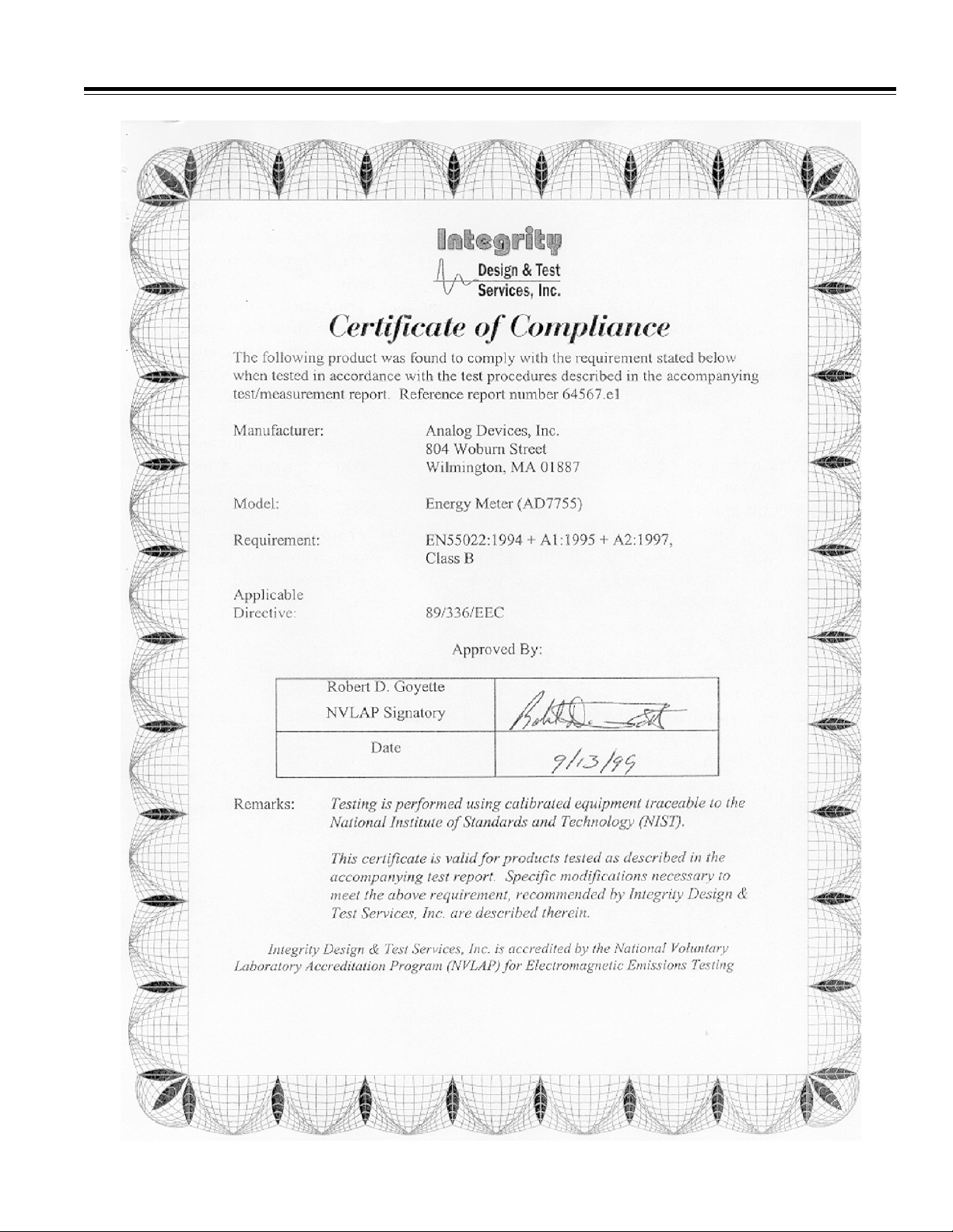
Figure 45. Certificate 1, Emissions Testing
–21–
Page 22

AN-559
E3742–2.5–6/00 (rev. A) 01017
Figure 46. Certificate 2, Susceptibility
–22–
PRINTED IN U.S.A.
REV. A
 Loading...