

Page 1
AN-533
a
APPLICATION NOTE
One Technology Way • P.O. Box 9106 • Norwood, MA 02062-9106 • 781/329-4700 • World Wide Web Site: http://www.analog.com
Applying the 5B Series Backplanes and Mounting Cards
VOLTAGE
I/O
+5V
POWER
CHANNEL
0
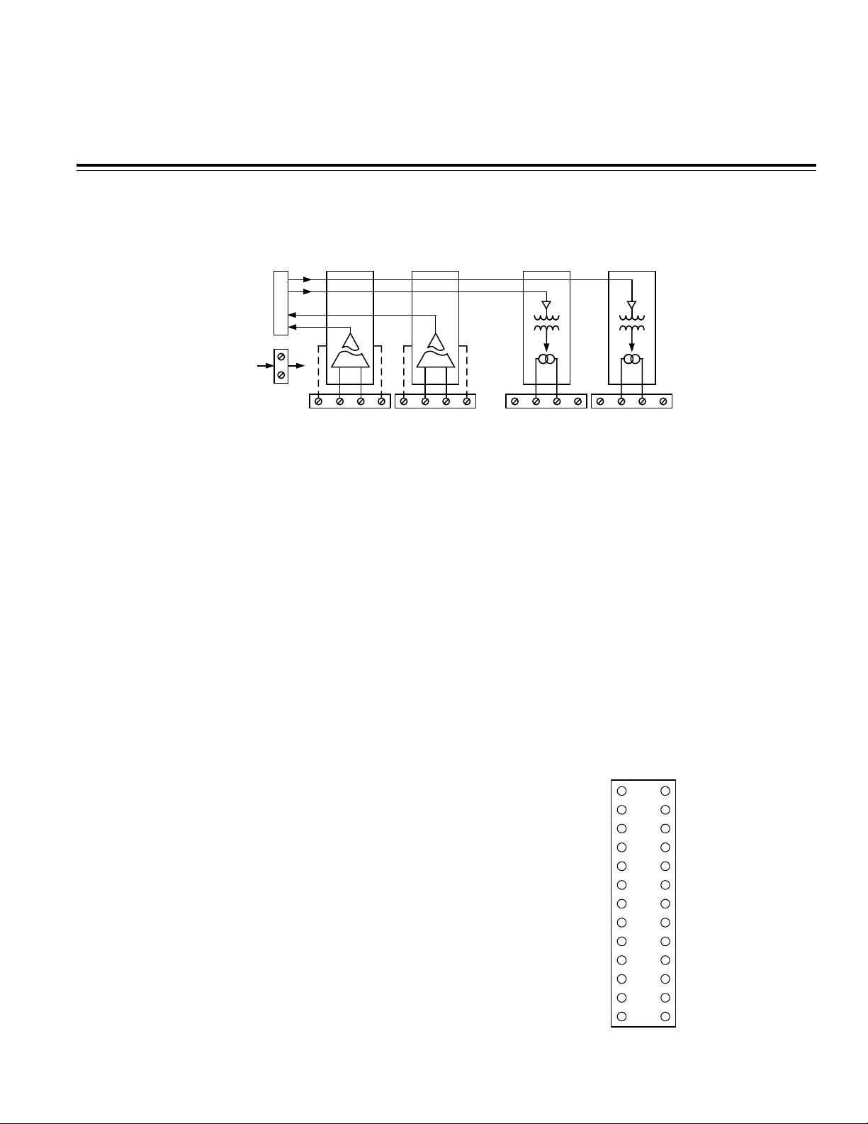
Figure 1. 5B01 Functional Block Diagram
INTRODUCTION
The 5B Series includes a number of multichannel
backplanes and mounting cards that provide a complete
signal conditioning solution. Four backplanes currently
available, the 16-channel 5B01 and 5B02 and the 8-channel 5B08 and 5B08-MUX, provide different system configuration options for the user. Models 5B01 and 5B08
I/O signals are independently available, while model
5B02 and 5B08-MUX I/O signals are controlled via an onboard multiplexer providing a bus for input signals and
a separate bus for output signals. With all backplanes,
5B Series modules can be mixed or matched and may be
changed without disturbing field wiring or system
power. The 5B03 and 5B04, one- and two-channel
mounting cards, allow an economical means to handle a
few remote signals. A single-channel mounting card,
AC1360, is available for ease of complete 5B Series
module evaluation.
Both 16-channel backplanes can be mounted in a
19" × 3.5" panel space, such as the rack mount kit, model
AC1393. The 8-channel backplanes can also be mounted
in the AC1393. The one- and two-channel mounting
cards, models 5B03, 5B04 and AC1360, are DIN rail compatible using available hardware. All backplanes and
mounting cards provide individual channel screw terminals for field connections. These connections satisfy all
transducer inputs and process current outputs and provide sensor excitation when necessary. A cold junction
temperature sensor, model AC1361, is supplied on each
channel to accommodate thermocouple modules (5B37
or 5B47). All backplanes and mounting cards require an
external regulated +5 V dc power supply.
CHANNEL
1
CHANNEL
14
CHANNEL
15
MODEL 5B01 BACKPLANE
The 5B01, diagrammed in Figure 1, is a 16-channel backplane that provides single-ended, high level analog
input/output pins on the system connector. It is pin compatible with Analog Devices’ 3B Series applications.
(Note, however, that 5B Series modules provide a ±5 V
output swing rather than the ±10 V swing provided by
3B Series modules.)
Model 5B01 System Connectors
Signal connections between the 5B01 backplane and the
associated measurement and control system are made
at P1 and P2. These connectors are identical electrically.
The redundant connectors may be useful if a 5B01 is
used for both analog input and analog output and the
data acquisition system has separate input and output
connectors. Figure 2 is a diagram of the voltage I/O
provided on the P1 and P2 connectors of the 5B01
backplane.
CH 0
COM
CH 1
CH 2
COM
CH 3
CH 4
COM
CH 5
CH 6
COM
CH 7
SENSE
1
3
5
7
9
11
13
15
17
19
21
23
25
TOP VIEW
NC = NO CONNECT
2
CH 8
4
CH 9
COM
6
CH 10
8
CH 11
10
COM
12
CH 12
14
CH 13
16
COM
18
CH 14
20
CH 15
22
24
COM
26
NC
Figure 2. 5B01 and 5B08 System Connector Pinout
Page 2
AN-533
FROM
CHANNEL
SELECT
LOGIC
POWER
FROM DAC
+5V
ADDRESS
DECODERS
4
4
TO A/D
16
16
OUTPUT ENABLE
INPUT ENABLE
OUTPUT BUS
INPUT BUS
. . . .
CHANNEL
0
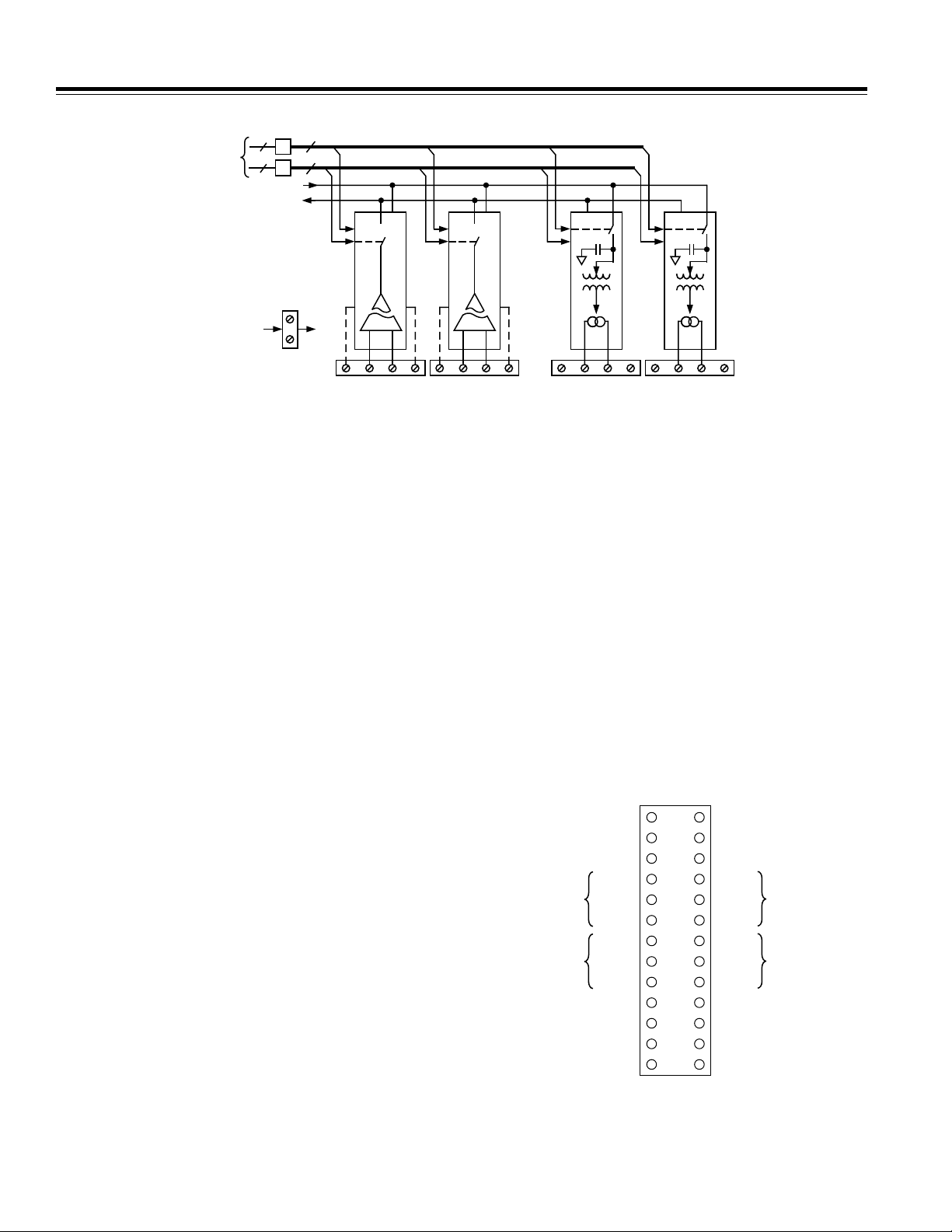
Figure 3. 5B02 Functional Block Diagram
A signal path is provided for each channel and, in addition, a number of grounding pins are present in the connector pinout to provide interchannel shield conductors
in the ribbon cable. In some cases, discussed below, the
ground conductors will not provide an accurate signal
reference, so a SENSE pin is also provided in the pinout.
Several jumper and component options on the backplane provide optimum ground connections for various
circumstances.
Model 5B01 Grounding
Each 5B01 backplane is factory configured with Jumpers
W1, W3 and W4 installed. Jumper W1 grounds the
shield wires in the ribbon cable (Pins 3, 6, 12, 15, 18, 21
and 24) at the 5B01 backplane. This will usually be the
primary ground connection between the 5B01 and the
measurement system. This connection is required if output modules will be used on the backplane. It is also required if there is no high impedance sense input (input
Low of a differential or pseudo-differential system)
available on the measurement system. Jumper W3 connects the sense input, if available, to Pin 25 so that the
5B01’s ground is read. It can be left in place at all times.
Jumper W4 connects +5 V dc power common to input/
output common (backplane measurement ground). A
connection between power common and input/output
common is important for the 5B Series modules to function properly; however, if this connection is made elsewhere in your system (the best place is usually near the
A/D or D/A converters), W4 should be cut, since a
ground loop could result.
Model 5B01 Interchannel Bridge Jumpers
The 5B01 gives the user the capability of directing the
voltage output of any input module to an adjacent output module (e.g., Model 5B39) simply by placing a
jumper between the pins of the two modules (input to
channel n, output from channel n + 1). This feature can
be used to provide an isolated current output from an
isolated input module, giving two levels of 1500 V rms
isolation. Model AC1344 provides ten jumpers.
CHANNEL
1
CHANNEL
14
CHANNEL
15
MODEL 5B02 BACKPLANE
The 5B02, diagrammed in Figure 3, is a 16-channel backplane. It incorporates input and output buses that take
advantage of the internal series output switches in the
input modules and the track-and-hold in the output
module. Designers integrating the 5B02 into a measurement and control system do not need external multiplexers and can use a single digital-to-analog converter
to serve numerous output channels. Digital outputs
from the host data acquisition system are used to address the 5B Series modules and designate inputs and
outputs. Only one analog input, one analog output, and
a number of digital outputs are required to address up to
64 analog input/output channels.
Model 5B02 System Connectors
Signal connections between the 5B02 backplane and the
associated measurement or control system are made at
P1. The pinout of this connector is illustrated in Figure 4.
1
V
READ
V
3
WRITE
I/O COM
READ
(INPUT)
ADDRESS
WRITE
(OUTPUT)
ADDRESS
READ ENB (0)
IS THE ANALOG OUTPUT OF INPUT MODULES
V
READ
V
IS THE ANALOG INPUT OF OUTPUT MODULES
WRITE
MATING CONNECTOR AMP PN746290-6 OR EQUIVALENT
LSB
BIT 3
BIT 5
LSB
BIT 3
BIT 5
NC
NC
D COM
5
7
9
11
13
15
17
19
21
23
25
TOP VIEW
NC = NO CONNECT
2
I/O COM
4
SNS LO
I/O COM
6
BIT 2
8
BIT 4
10
MSB
12
BIT 2
14
BIT 4
16
MSB
18
WRITE ENB (0)
20
RESERVED
22
24
NC
26
D COM
READ
(INPUT)
ADDRESS
WRITE
(OUTPUT)
ADDRESS
Figure 4. 5B02 System Connector Pinout
–2–
Page 3
AN-533
SH
1
2
3
4
5
SH
6
7
8
9
10
One signal path is provided for inputs and one for outputs. Input and output modules are independently addressed by two sets of six address pins and an enable
pin. In addition, a number of grounded pins are present
in the connector pinout to provide shield conductors in
the ribbon cable. In some cases, discussed below, the
ground conductors will not provide an accurate signal
reference, so a SENSE pin is also provided in the pinout.
ignored. Moving the jumpers to any other position in the
two blocks enables decoding of the full six address bits;
the exact position of the jumper determines address
position for the backplane as shown in Table I. To use
multiple backplanes in this manner, connect the corresponding I/O connector pins of each backplane in
parallel. CAB-01 is a ribbon cable with three 26-pin con-
nectors designed for this purpose.
Several jumper and component options in the backplane provide optimum ground connections for various
circumstances.
Model 5B02 Grounding
Each 5B02 backplane is factory configured with Jumpers
W1, W2 and W4 installed. Jumper W1 grounds the
shield wires in the ribbon cable (Pins 2, 5 and 6) at the
5B02 backplane. This will usually be the primary ground
connection between the 5B02 and the measurement
system. This connection is required if output modules
will be used on the backplane. It is also required if there
Figure 5. 5B02 Address Selection Pins Shown with
Factory Default Jumpers
is no high impedance sense input (input low of a differential or pseudo-differential system) available on the
measurement system. Jumper W2 connects the sense
input, if available, to Pin 25 so that the 5B02’s ground is
read. It can be left in place at all times. Jumper W4 connects +5 V dc power common to input/output common
(backplane measurement ground). A connection between power common and input/output common is im-
Input Jumper Output Jumper Address Range
2 7 48–63
3 8 32–47
4 9 16–31
5 10 0–15
Table I. 5B02 Address Selection Jumpers
portant for the 5B Series modules to function properly;
however, if this connection is made elsewhere in your
system (the best place is usually near the A/D or D/A
converters), W4 should be cut since a ground loop could
result.
Model 5B02 Address Selection Jumpers
The 5B02 backplane can hold 16 modules in any combination of inputs or outputs. Address decoders on the
backplane (separate decoders are provided for inputs
and outputs) determine which module is read (inputs) or
driven (outputs). To permit system expansion, up to four
backplanes can be daisy-chained on the system I/O ribbon cable for a total of 64 channels. Jumpers on each
backplane (labeled SH1-5 and SH6-10) determine the
block of 16 addresses assigned to each backplane. Input
(read) and output (write) addressing are completely independent; in all cases, Jumpers 1–5 control inputs and
6–10 control outputs. Independent addressing might be
used, for example, to update output modules without
interrupting the monitoring of input modules.
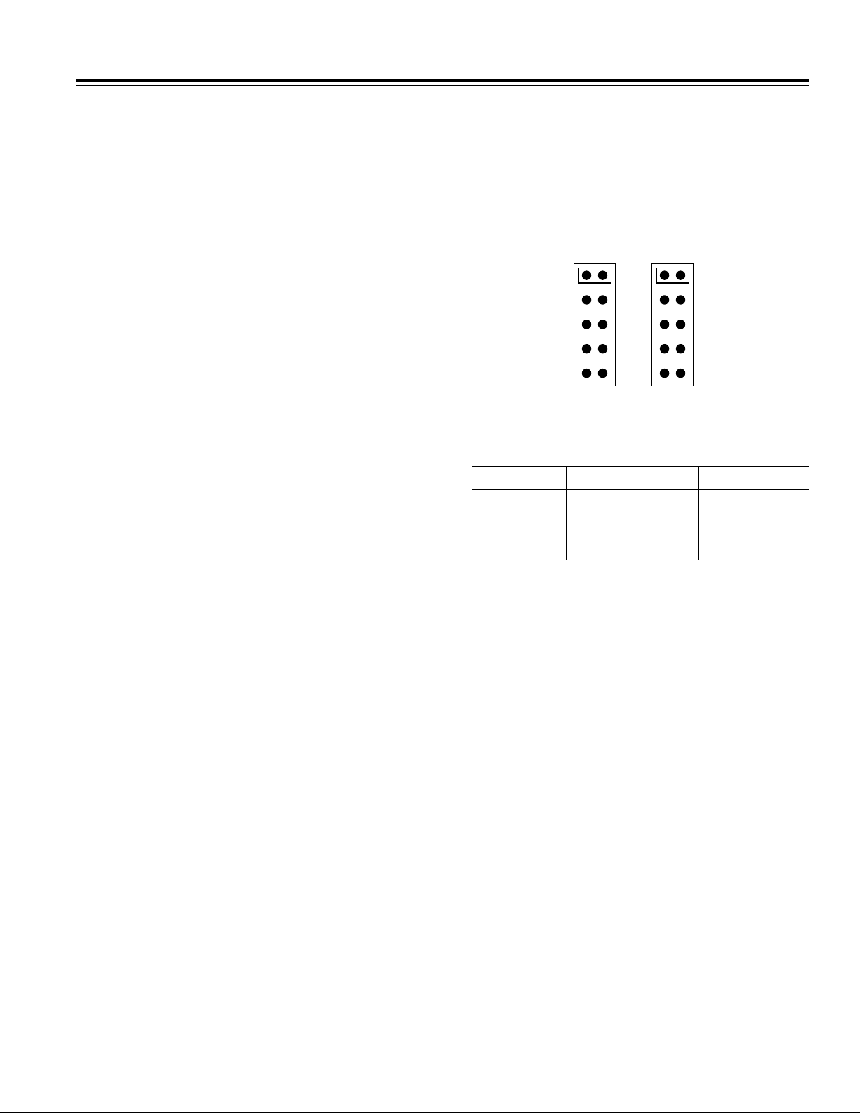
Backplanes are factory configured with jumpers at Positions 1 and 6; Figure 5 shows the address jumpers in the
MODEL 5B08 BACKPLANE
Model 5B08 System Connectors
Signal connections between the 5B08 and the associ-
ated measurement and control system are made with
two identical 26-pin connectors (P1 and P2), similar to
the 16-channel model 5B01 backplane. Reference to
these connectors is electrically identical and may be
useful if a 5B08 is used for both analog input and analog
output and the data acquisition system has separate in-
put or output connectors. Figure 2, shown with model
5B01, illustrates the pin assignments for P1 and P2.
The I/O connectors provide a signal path for each chan-
nel and, in addition, a number of grounding pins are
available to provide interchannel shield conductors in
the ribbon cable. In some cases, discussed below, the
ground conductors will not provide an accurate signal
reference, so a SENSE pin is also provided in the con-
nectors. Several jumper and component options on the
5B08 provide optimum ground connections for various
applications. These are discussed in the following
sections.
factory configured positions. This sets up the backplane
as a stand-alone 16-channel system; the two highestorder address bits in the read and write addresses are
–3–
Page 4

AN-533
Model 5B08 Output Channel Selection
To configure Model 5B08 I/O for different system needs,
on-board jumpers are provided. A family of eight 3-pin
jumpers, J8 through J15, allows the user to assign the
5B08 I/O to either the upper eight I/O pins (CH0, CH1,
CH2, CH3, CH4, CH5, CH6, CH7) or to the lower eight I/O
pins (CH8, CH9, CH10, CH11, CH12, CH13, CH14, CH15).
This capability allows two 8-channel 5B08 backplanes to
be used in a 16-channel configuration, with all I/O assigned to the 16 unique I/O pins, CH0–CH15. Table II illustrates the channel assignments for each of the eight
Jumpers, J8 through J15.
Table II. 5B08 Output Channel Assignments
Jumper To V/I
Jumper Position Connects Channel
J8 LO Channel 0 0
HI 8
J9 LO Channel 1 1
HI 9
J10 LO Channel 2 2
HI 10
J11 LO Channel 3 3
HI 11
J12 LO Channel 4 4
HI 12
J13 LO Channel 5 5
HI 13
J14 LO Channel 6 6
HI 14
J15 LO Channel 7 7
HI 15
Model 5B08 Interchannel Jumpers
The 5B08 offers the user the ability to easily connect the
voltage output of any 5B Series input module directly to
the voltage input of an adjacent output module (e.g.,
Model 5B39) by placing a jumper over two pins J1, J2,
J3, J4, J5, J6 or J7. This feature can be used to provide
an isolated current output from an isolated input module. This results in both isolated voltage and isolated
current outputs from a single sensor input signal. A kit
of ten jumpers is available as Model AC1344. Table III
shows the channel assignments when Jumpers J1–J7
are used. Additional configuration flexibility is provided
when the output jumper selections (J8–J15) are combined with the interchannel jumper selections (J1–J7).
Table III provides the resulting signal assignments for
each of the various jumper selections.
Table III. 5B08 Interchannel Jumpers
Jumper Connects
J1 Channel 0 to V
J2 Channel 1 to V
J3 Channel 2 to V
J4 Channel 3 to V
J5 Channel 4 to V
J6 Channel 5 to V
J7 Channel 6 to V
to Channel 1 V
OUT
to Channel 2 V
OUT
to Channel 3 V
OUT
to Channel 4 V
OUT
to Channel 5 V
OUT
to Channel 6 V
OUT
to Channel 7 V
OUT
IN
IN
IN
IN
IN
IN
IN
Table IV. 5B08 Channel Assignments Using Output and
Interchannel Jumpers
Jumper Output Channel Connects
Closed Jumper Setting Connects V/I Channels
J1 J8 LO J9 LO Channel 0 0 to 1
J8 HI J9 LO to 8 to 1
J8 LO J9 HI Channel 1 0 to 9
J8 HI J9 HI 8 to 9
J2 J9 LO J10 LO Channel 1 1 to 2
J9 HI J10 LO to 9 to 2
J9 LO J10 HI Channel 2 1 to 10
J9 HI J10 HI 9 to 10
J3 J10 LO J11 LO Channel 2 2 to 3
J10 HI J11 LO to 10 to 3
J10 LO J11 HI Channel 3 2 to 11
J10 HI J11 HI 10 to 11
J4 J11 LO J12 LO Channel 3 3 to 4
J11 HI J12 LO to 11 to 4
J11 LO J12 HI Channel 4 3 to 12
J11 HI J12 HI 11 to 12
J5 J12 LO J13 LO Channel 4 4 to 5
J12 HI J13 LO to 12 to 5
J12 LO J13 HI Channel 5 4 to 13
J12 HI J13 HI 12 to 13
J6 J13 LO J14 LO Channel 5 5 to 6
J13 HI J14 LO to 13 to 6
J13 LO J14 HI Channel 6 5 to 14
J13 HI J14 HI 13 to 14
J7 J14 LO J15 LO Channel 6 6 to 7
J14 HI J15 LO to 14 to 7
J14 LO J15 HI Channel 7 6 to 15
J14 HI J15 HI 14 to 15
–4–
Page 5

AN-533
Model 5B08 Grounding
Model 5B08 is supplied with three grounding jumpers:
W1, W3 and W4. These three jumpers are installed at the
factory, but can be changed to accommodate user system configuration needs. Jumper W1 connects the P1
and P2 shield pins 3, 6, 9, 12, 15, 18, 21 and 24) to the
5B08 I/O common (backplane measurement ground).
This will usually be the primary ground connection between the 5B08 backplane and the measurement system. This connection is required if output modules are
used on the 5B08. It is also required if there is no high
impedance sense input (input LOW of a differential (or
pseudo-differential system) available on the measurement system. Jumper W3 connects the sense input, if
available on Pin 25, to the 5B08 I/O common, so it can be
read directly. W3 can be left in place at all times. Jumper
W4 connects the 5B08 I/O common to the +5 V dc power
common. A connection between power common and I/O
common is important for the 5B Series modules1 to
function properly; however, if this connection is made
elsewhere in your system (the best place is usually near
the A/D or D/A converters), W4 should be cut since a
ground loop could result.
MODEL 5B08-MUX BACKPLANE
The 5B08-MUX incorporates input and output buses that
take advantage of the internal series output switches in
the 5B Series input modules as well as the track-and
hold circuit in the output modules. Designers integrating the 5B08-MUX into a measurement and control system do not need external multiplexers and can use a
single digital-to-analog converter to serve numerous
output channels. Refer to Figure 6 for a functional block
diagram of model 5B08-MUX. Digital outputs from the
host data acquisition system are used to address the 5B
Series modules and designate inputs and outputs. Only
one analog input, one analog output and a number of
digital outputs are required to address up to 64 analog
input/output channels using eight 5B08-MUX backplanes.
Model 5B08-MUX System Connectors
Signal connections between the 5B08-MUX and the as-
sociated measurement or control system are made at
P1, a 26-pin connector, similar to the 5B02 backplane.
The pinout of P1 is shown in Figure 4.
One signal path is provided for inputs and one for out-
puts. Input and output modules are independently ad-
dressed by two sets of six address pins and an enable
pin. In addition, a number of grounded pins are present
in the connector pinout to provide shield conductors in
the ribbon cable. In some cases, discussed below, the
ground conductors will not provide an accurate signal
reference, so a SENSE pin (SNS LO) is also provided in
the pinout. Several jumper and component options on
the backplane provide optimum ground connections for
various circumstances.
Model 5B08-MUX Grounding
Model 5B08-MUX is supplied with three grounding
jumpers: W1, W2 and W4. These three jumpers are
installed at the factory, but can be changed to accommo-
date user system configuration needs. Jumper W1 con-
nects the P1 shield pins (Pins 2, 5 and 6) to the
5B08-MUX backplane common (backplane measure-
ment ground). This will usually be the primary ground
connection between the 5B08-MUX backplane and the
measurement system. This connection is required if out-
put modules are used on the 5B08-MUX. It is also re-
quired if there is no high impedance sense input (input
LO of a differential or pseudo-differential system) avail-
able on the measurement system. Jumper W2 connects
the sense input from the measurement system, if avail-
able on Pin 4, to the 5B08-MUX backplane common, so it
can be read directly. W2 can be left in place at all times.
Jumper W4 connects the 5B08-MUX backplane com-
mon to the +5 V dc power common. A connection be-
tween power common and I/O common is important for
the 5B Series modules to function properly; however, if
FROM
CHANNEL
SELECT
LOGIC
POWER
FROM DAC
+5V
ADDRESS
DECODERS
4
TO A/D
84
8
OUTPUT ENABLE
INPUT ENABLE
OUTPUT BUS
INPUT BUS
. . . .
CHANNEL
0
Figure 6. 5B08-MUX Functional Block Diagram
CHANNEL
1
–5–
CHANNEL
7
CHANNEL
8
Page 6

AN-533
this connection is made elsewhere in your system (the
best place is usually near the A/D or D/A converters), W4
should be cut since a ground loop could result.
Model 5B08-MUX Address Jumpers
5B08-MUX backplane can hold eight 5B Series modules
in any combination of inputs or outputs. Address decoders on the backplane determine which module is read
(input type) or driven (output type). Separate decoders
are provided for inputs and outputs. To permit system
expansion, up to eight 5B08-MUX backplanes can be
daisy-chained on the system I/O ribbon cable for a total
of 64 channels. Jumpers on each backplane (labeled J1–
J9 and J10–J18) determine the block of eight addresses
assigned to each backplane. Input (read) and output
(write) addressing are completely independent; in all
cases, Jumpers J1–J9 control inputs and J10–J18 control outputs. Independent addressing might be used, for
example, to update output modules without interrupting
the monitoring of input modules.
Table V. 5B08-MUX Address Jumpers
Input Jumper Output Jumper Address Range
J2 J11 56–63
J3 J12 48–55
J4 J13 40–47
J5 J14 32–39
J6 J15 24–31
J7 J16 16–23
J8 J17 8–15
J9 J18 0–7
5B08-MUX Factory Jumper Settings
5B08-MUX backplanes are factory configured with
jumpers at Positions J1 and J10. This sets up the 5B08MUX backplane as a stand-alone 8-channel system.
Moving the jumpers to any other position in the two
blocks of jumpers enables decoding of the full six address bits; the exact position of the jumper determines
address position for the 5B08-MUX backplane as shown
in Table V. To use multiple 5B08-MUX backplanes in this
manner, connect the corresponding I/O connector pins
of each backplane in parallel. Model CAB-01 cable is a
ribbon cable with three 26-pin connectors designed for
this purpose.
MODEL 5B01, 5B02, 5B08 AND 5B08-MUX GROUND STUDS
The 5B Series modules meet transient voltage protection standard ANSI/IEEE C37.90.1-1989, thereby preventing harm to the connected system even when a very
large, fast transient strikes all field I/O lines at the same
time. However, proper grounding of the backplane is
essential to get full protection since in such cases currents on the order of an ampere with rise times on the
order of one microsecond must be diverted to ground.
Both the resistance and the inductance of the ground
path are critical. In applications where hazards of this
magnitude exist, the large (#10-32) ground studs provided at each end of the 5B01, 5B02, 5B08 and 5B08MUX backplanes should be connected to system ground
by the shortest practical length of large-diameter wire.
The surge withstand capability can be tested with not
less than fifty 2.5 kV bursts per second. A test duration of
two seconds is widely accepted. A rise time of 20 kV/µs
is specified, and each module could see a surge current
on the order of 1 ampere.
When a safety ground is used, the connection of backplane measurement ground to system measurement
ground via the shield wires in the ribbon cable could result in a ground loop. If the application involves only input modules and a sense input is used on the
measurement system, W1 should be cut to prevent a
ground loop.
Caution:
W1 is required if output modules are used or
there is no high impedance sense input on the measurement system. In these cases, the best defense against
ground loop effects is to minimize the distance between
the backplane and the associated system and to route
any large currents carefully so as to minimize ground
differences.
MODELS 5B01, 5B02, 5B08 AND 5B08-MUX FUSING AND
SUPPLY VOLTAGE
All 5B Series backplanes require external +5 V dc regulated power. This is connected directly to the designated
supply input screw terminals. The power supply is
bused to all signal conditioners on the backplane. The
total subsystem power requirement is a function of the
modules that are used. Since reversing the polarity of
the connected +5 V dc power source could destroy installed modules, the 5B01, 5B02, 5B08 and 5B08-MUX
backplanes incorporate polarity reversal protection in
the form of a shunt diode. A series fuse will be blown by
the diode current if the supply is reversed. If the fuse is
blown, replacement with the proper type (Littelfuse
type 252 004) is essential.
®
Littelfuse is a registered trademark of Littelfuse, Inc.
–6–
Page 7

AN-533
MODELS 5B03 AND 5B04 MOUNTING CARDS
The 5B03 card holds one 5B Series module, the 5B04
holds two modules. These cards may be clustered for
larger groups of modules.
Refer to Figures 7 and 8 for the wiring diagrams for the
5B03 and 5B04.
OUT
/V
IN
V
+5V DC
I/O COM
PWR COM
4 3 2 1
POWER
TEMP
SENSOR
W1
–EXC
LO
4321
HI
+EXC
LOCAL I/O
SOCKET FOR AC1362 CURRENT
CONVERSION RESISTOR
USED WITH 5B32 MODULES
ISOLATED I/O
Figure 7. Model 5B03 Wiring Diagram
Models 5B03 and 5B04 Grounding
Jumper W1 connects +5 V dc power common to input/
output common (backplane measurement ground). A
connection between power common and input/output is
important for the 5B Series modules
to function properly; however, if this connection is made elsewhere in
your system (the best place is usually near the D/A or
A/D converters), W1 should be cut since a ground loop
could result.
Models 5B03 and 5B04 DIN Rail Mounting
Individual mounting cards are DIN rail compatible using
Phoenix Universal Mounting UM modules. Two or more
cards can be mounted in wider UM assemblies. The
snap foot elements will fit DIN EN 50022, DIN EN 50035,
and DIN EN 50045 rails.
Mounting a single 5B03 or 5B04 would require the
Phoenix parts listed in Table VI.
Table VI. 5B03 and 5B04 Phoenix DIN Rail Mounting Parts
Phoenix Model Description Qty.
UM-BEFE Base Element with Snap Foot 1
UM-SE Side Element 2
Mounting two or more 5B03 or 5B04 cards would require the parts listed in Table VII. The (#) is the total
number of 5B03 and 5B04 mounting cards to be DIN rail
mounted.
POWER
ISOLATED I/O
– CH A
– CH B
OUT
OUT
/V
/V
IN
IN
V
V
I/O COM
PWR COM
–EXC
LO
+EXC
+5V DC
12
12
34
HI
W1
21
3
LOCAL I/O
TEMP
SENSOR
+EXC
4321
HI
LO
–EXC
SOCKETS FOR AC1362 CURRENT
CONVERSION RESISTORS
USED WITH 5B32 MODULES
Figure 8. Model 5B04 Wiring Diagram
Table VII. Phoenix DIN Rail Mounting Parts For Multiple
5B03 and 5B04
Phoenix
Model Description Qty.
UM-BEFE Base Element with Snap Foot 2
UM-SE Side Element 2
UM-BE Base Element (#) – 2
UM-VS Connection Pins (4 × (#)) – 4
Power Connection
The 5B03 and 5B04 are powered with a single +5 V dc
supply, applied to terminals +5 V and +PWR COM.
Caution:
The 5B03 and 5B04 are not protected against
reversed power supply connections. A reversal may destroy the installed modules.
MODEL AC1360 MOUNTING CARD
The AC1360 is a 1-channel test or evaluation mounting
card for the 5B Series modules. Screw terminals are
provided for all of the module’s input, output, control
and power connections. In addition, the AC1361 cold
–7–
Page 8

AN-533
junction temperature sensor is installed for thermocouple applications, and a pair of sockets permits installation of the AC1362 current sensing resistor used with
the 5B32 current input module.
CONTROL
RD EN
WR EN
DATA
P.COM
+5V
P.COM
ISOLATED I/O
–EXC LO HI +EXC
LOCAL I/O
W1
W2
CJC
V
OUT
IO COM
V
IO COM
IN
Figure 9. AC1360 Mounting Card
Model AC1360 DIN Rail Mounting
The AC1360 is DIN rail mountable, using Phoenix Universal Module UM elements. To mount a single AC1360
would require the following Phoenix parts:
Table VIII. Phoenix DIN Rail Mounting Parts For Model
AC1360
Phoenix Model Description Qty.
UM-BEFE Base Element with Snap Foot 2
UM-SE Side Element 2
UM-VS Connection Pins 4
Standoffs are included with each AC1360 for bench top
use or wall mounting.
Model AC1360 Configuration Jumpers
The AC1360 includes two configuration jumpers. The
first, labeled W1, is factory installed and provides a convenient point for providing the required current return
path from I/O common on the nonisolated (system side)
of the modules to the +5 V supply common. In general,
this is not the best place to have such a connection. In
most applications, there will already be a suitable path
resulting from a connection at another point so that W1
will result in a ground loop. Virtually any contact between supply common and analog measurement common in the surrounding system is sufficient; the two
grounds can be several volts apart and can have a resis-
tance of up to 10 kΩ between them without affecting 5B
Series module operation. W1 should be cut if such a
contact exists.
Jumper W2 is also factory installed and only affects the
operation of thermocouple input modules. W2 connects
the AC1361 temperature sensor in its normal manner
when a thermocouple input module is installed in the
module socket. For applications involving connection of
thermocouple wire to the HI and LOW screw terminals,
this results in normal correction in the module for the
thermal effects of the connections. If, however, a 5B37
or 5B47 thermocouple module is to be operated without
thermocouple wire at the screw terminals—as, for example, in a test fixture using a millivolt source—the temperature sensor must be disabled and a suitable voltage
to simulate operation at a chosen terminal temperature
must be substituted. This is accomplished by opening
jumper W2 and connecting a voltage source to the terminals labeled CJC (Cold Junction Compensation). The
required polarity of the applied voltage is indicated at
the terminals. It is absolutely essential that the source of
the voltage floats with respect to anything connected to
the HI and LOW input terminals (or the ±EXC screws,
which are not normally used in thermocouple applications). Most bench top calibration sources have the necessary isolation to work properly. In these applications,
a CJC voltage of 510.0 mV will simulate sensor opera-
tion at a terminal temperature of +25°C. Since there are
no parasitic thermocouples at the screw terminals to
correct, all output readings will appear to be 25°C higher
than would be implied by the input voltage. With the
25°C shift taken into account, however, module opera-
tion is close to normal conditions for test or evaluation
purposes. Alternatively, a CJC voltage of 572.5 mV can
be applied, simulating operation at a terminal tempera-
ture of 0°C. Millivolt inputs can then be read directly
from thermocouple tables without any temperature
shift. At 572.5 mV, however, since the module’s cold
junction correction circuitry is operating far from its design center, its errors will be larger than would be the
case in normal operation.
Power Connection.
The AC1360 is powered with a single +5 V dc supply,
applied to terminals +5 V and P.COM.
Caution:
The AC1360 is not protected against reversed
power supply connections. A reversal may destroy the
installed module.
E3283–5–4/98
PRINTED IN U.S.A.
–8–
 Loading...