

Page 1
AN-369
a
APPLICATION NOTE
One Technology Way • P.O. Box 9106 • Norwood, MA 02062-9106 • 781/329-4700 • World Wide Web Site: http://www.analog.com
Thermocouple Signal Conditioning Using the AD594/AD595
by Joe Marcin
INTRODUCTION
One of the most widely used devices for temperature
measurement is the thermocouple. Whether in an industrial, commercial or scientific application, a thermocouple offers a cost effective solution to temperature
measurements in many environments over wide temperature ranges. Unfortunately, their basic principles
are often misunderstood resulting in serious measurement errors. This application note will review thermocouple fundamentals and illustrate circuit designs for
thermocouple signal conditioning using the AD594/
AD595 monolithic IC.
BACK TO BASICS
The basic principles of the thermocouple were discovered in 1821 by Thomas Seebeck. When two dissimilar
metals are joined at both ends and one end is heated, a
current will flow. If the loop is broken at the center, an
open circuit voltage (the Seebeck Voltage) is generated
and is proportional to the difference in temperature between the two junctions. Therefore, in determining the
temperature of the measuring junction, the reference
junction temperature must be known.
V
– V
T1
T2
MEASURING
JUNCTION
T1 T2
A
V
T1
B
A
V
T2
B
REFERENCE
JUNCTION
Figure 1a. Thermocouple Loop
An ice bath provides a well defined temperature of 0°C
for the reference junction. This has become a standard
reference point for the thermocouple output voltage vs.
temperature tables for various metal combinations.
V
(V
= 0)
T1
T2
T2 = 08C
V
T2
MEASURING
JUNCTION
T1
A
V
T1
B
A
B
These combinations have been characterized and classified by the National Institute of Standards and Technology (formerly the National Bureau of Standards). The
table below lists the types, composition and characteristics of the more commonly used thermocouples.
Table I. Thermocouple Properties
ANSI Alloy Temperature mV
Code Combination Range Output
B Platinum/Rhodium 0°C to +1700°C 0 to +12.426
E Chromel/Constantan –200°C to +900°C –8.824 to +68.783
J Iron/Constantan 0°C to +750°C 0 to +42.283
K Chromel/Alumel –200°C to +1250°C –5.973 to +50.633
N Nicrosil/Nisil –270°C to +1300°C –4.345 to +47.502
R Platinum/Rhodium 0°C to +1450°C 0 to +16.741
Platinum
S Platinum/Rhodium 0°C to +1450°C 0 to +14.973
Platinum
T Copper/Constantan –200°C to +350°C –5.602 to +17.816
Maximum
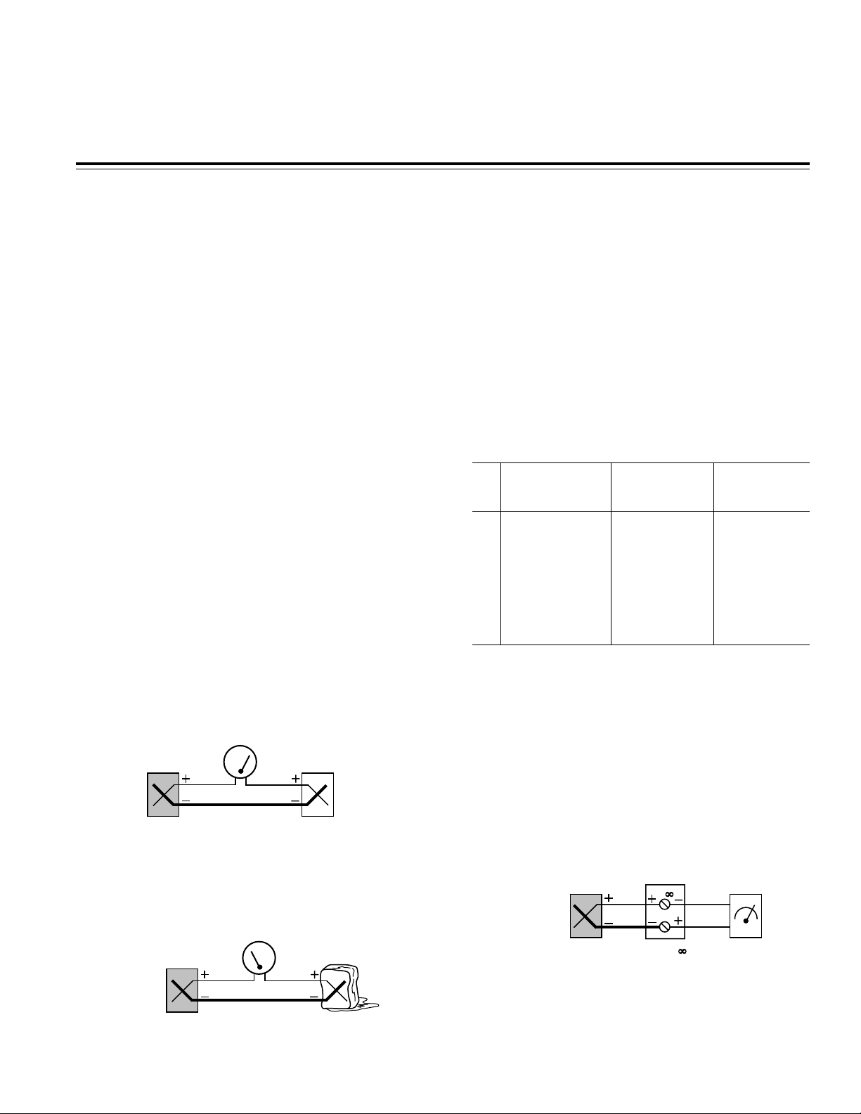
A voltmeter is commonly used to measure the Seebeck
voltage; however, great care must be exercised when interconnecting it to the thermocouple. Referring to Figure 1c, two additional junctions, J2 and J3, are formed at
the connection between the thermocouple and meter.
These two junctions produce opposing voltages within
the thermocouple loop. Using an isothermal block at the
point of connection keeps these junctions in thermal
equilibrium and produces equal but opposite emfs. The
measured voltage now is the difference in potential between the measuring junction and the isothermal block
which serves as the reference junction.
T2
V
A
V
B
B
(VT2 = VBA = V+VB)
Cu
Cu
– V
V
T1
T2
MEASURING
JUNCTION
T1
V
T1
Figure 1c. Measuring a Thermocouple Voltage with a
Voltmeter
Figure 1b. Ice Point Reference
Page 2
AN-369
PRACTICAL THERMOCOUPLE MEASUREMENT
For most applications, it is impractical to use an ice bath
for the reference junction. By compensating for the voltage developed at the reference junction, the ice point
reference may be eliminated. This is performed by adding a voltage into the thermocouple loop, equal but opposite to that of the reference junction. A circuit that
provides cold junction compensation along with amplification and open thermocouple detection is included in
the AD594/AD595 family of thermocouple signal conditioning ICs.
T2
A
B
Cu
V
COMP
Cu
Cu
VT1 – VT2 + V
(V
– VT2)
COMP
COMP
MEASURING
JUNCTION
T1
V
T1
Figure 1d. Cold Junction Compensation
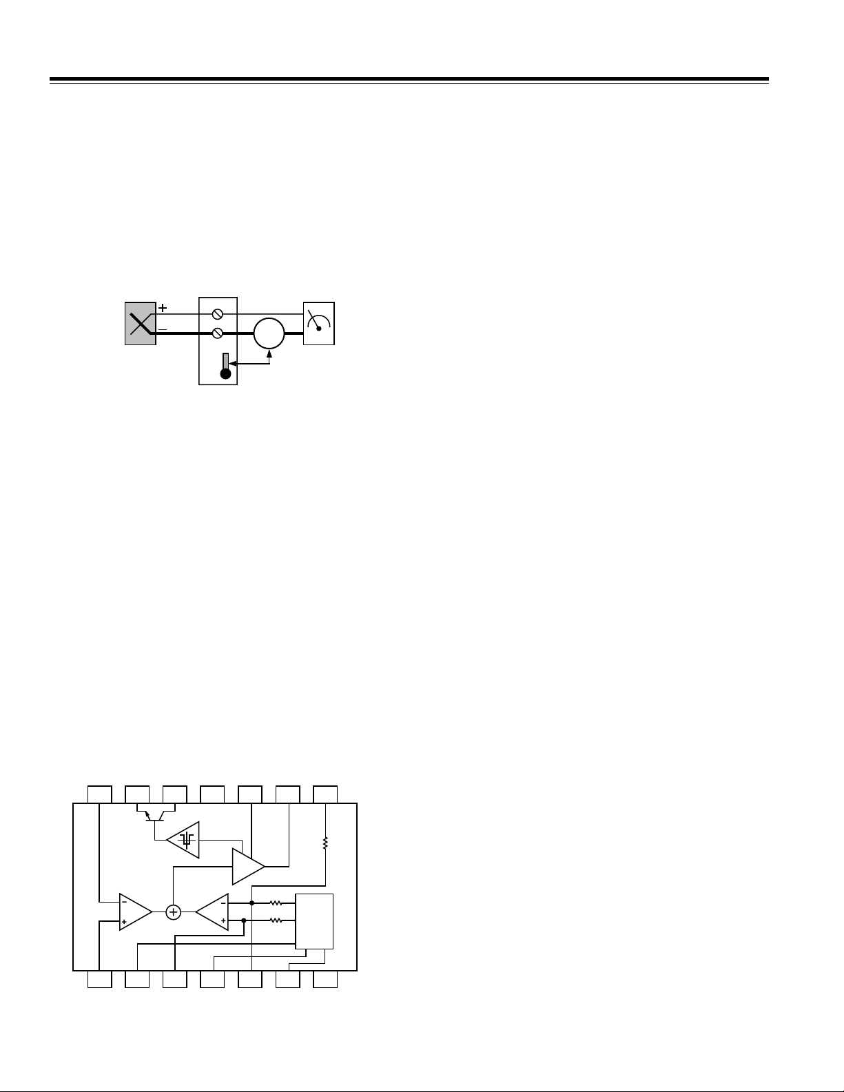
THE AD594/AD595 CIRCUIT DESCRIPTION
Figure 2 is a block diagram of the AD594/AD595 thermocouple signal conditioner IC. A Type J (for the AD594) or
Type K (for the AD595) thermocouple is connected to
Pins 1 and 14, the inputs to an instrumentation amplifier
differential stage. This input amplifier is contained in a
loop that uses the local temperature as its reference.
With the IC also at the local temperature, an ice point
compensation circuit develops a voltage equal to the deficiency in the locally referenced thermocouple loop.
This voltage is then applied to a second preamplifier
whose output is summed with the output of the input
amplifier. The resultant output is then applied to the input of a main output amplifier with feedback to set the
gain of the combined signals. The ice point compensation voltage is scaled to equal the voltage that would be
produced by an ice bath referenced thermocouple measuring the IC temperature. This voltage is then summed
with the locally referenced loop voltage, the result being
a loop voltage with respect to an ice point.
–IN –ALM +ALM V+ COMP V
14 13 12 11 10 9 8
OVERLOAD
DETECT
AD594/
AD595
+A
FB
O
Through the feedback path, the main amplifier maintains a balance at its inputs. In the event of a broken
thermocouple or open circuit at the device’s input, these
inputs become unbalanced, the fault is detected, and the
overload detection circuit drives a current limited n-p-n
transistor that may be interfaced as an alarm.
Although these ICs are specifically calibrated for a Type
J or K thermocouple, other thermocouple types may be
used with recalibration. Pin connections to internal
nodes for the temperature controlled voltages and feedback are provided to perform recalibration.
INTERPRETING AD594/AD595 OUTPUT VOLTAGES
To produce a temperature proportional output of
10 mV/°C, and provide an accurate reference junction
over the rated operating temperature range, the AD594/
AD595 is gain trimmed at the factory to match the transfer characteristics of Type J and K thermocouples at
+25°C. At this calibration temperature, the Seebeck coef-
ficient, the rate of change of thermal voltage with
respect to temperature at a given temperature, is
51.70 µV/°C for a Type J thermocouple and 40.44 µV/°C
for a Type K. This corresponds to a gain of 193.4 for the
AD594 and 247.3 for the AD595 to realize a 10 mV/°C out-
put. Although the device is trimmed for a 250 mV output
at +25°C, an input offset error is induced in the output
amplifier resulting in offsets of 16 µV and 11 µV for the
AD594/AD595 respectively. To determine the actual output voltage from the AD594/AD595, the following equations should be used:
AD594 Output
AD595 Output
= (
Type J Voltage
= (
Type K Voltage
+ 16 µV) × 193.4
+ 11 µV) × 247.3
where the Type J and K voltage are taken from the
thermocouple voltage tables referred to zero degrees
Celsius.
It is important to note that a thermocouple’s output is
linear over a narrow temperature range. Over a wide
temperature range, the Seebeck coefficient introduces
nonlinearity. Linearization is not provided by the AD594/
AD595, and any linearization techniques must be performed externally. This entails calculating thermocouple temperature using high order polynomials. The
National Institute of Standards and Technology offers
tables of polynomial coefficients for a given thermocouple type which may be used in this process.
G
1234567
+IN +C +T COM V––T –C
G
+TC
ICE
POINT
COMP.
–TC
Figure 2. AD594/AD595 Functional Block Diagram
–2–
Page 3
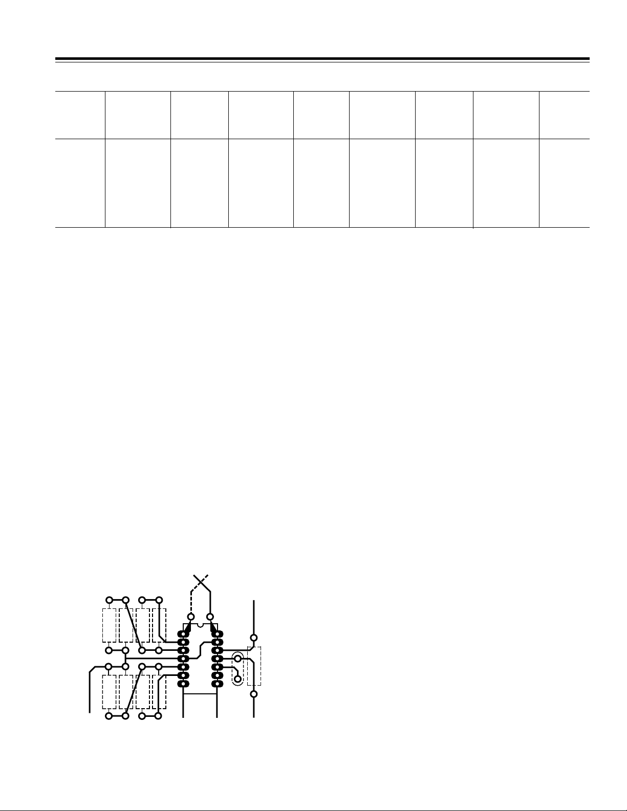
Table II. Calculated Errors at Various Ambient Temperatures
AN-369
Ambient Temp. Rej. Total Temp. Rej. Total Temp. Rej. Total Temp. Rej. Total
AD594C AD594C AD594A AD594A AD595C AD595C AD595A AD595A
Temp. Error Error Error Error Error Error Error Error
ⴗC ⴗC ⴗC ⴗC ⴗC ⴗC ⴗC ⴗC ⴗC
–55 4.83 5.83 6.83 9.83 5.28 6.28 7.28 10.28
–25 1.98 2.98 3.23 6.23 2.04 3.04 3.29 6.29
0 0.62 1.62 1.25 4.25 0.62 1.62 1.25 4.25
+25 0.00 1.00 0.00 3.00 0.00 1.00 0.00 3.00
+50 0.62 1.62 1.25 4.25 0.62 1.62 1.25 4.25
+70 1.46 2.46 2.59 5.59 1.38 2.38 2.50 5.50
+85 2.25 3.25 3.75 6.75 1.99 2.99 3.49 6.49
+125 4.90 5.90 7.40 10.40 3.38 4.38 5.88 8.88
NOTE
Temp. Rej. Error has two components: (a) Difference between actual reference junction and ice point compensation voltage times the gain; (b) Offset and
gain TCs extrapolated from 0°C to +50°C limits. Total error is temp. rej. plus initial calibration error.
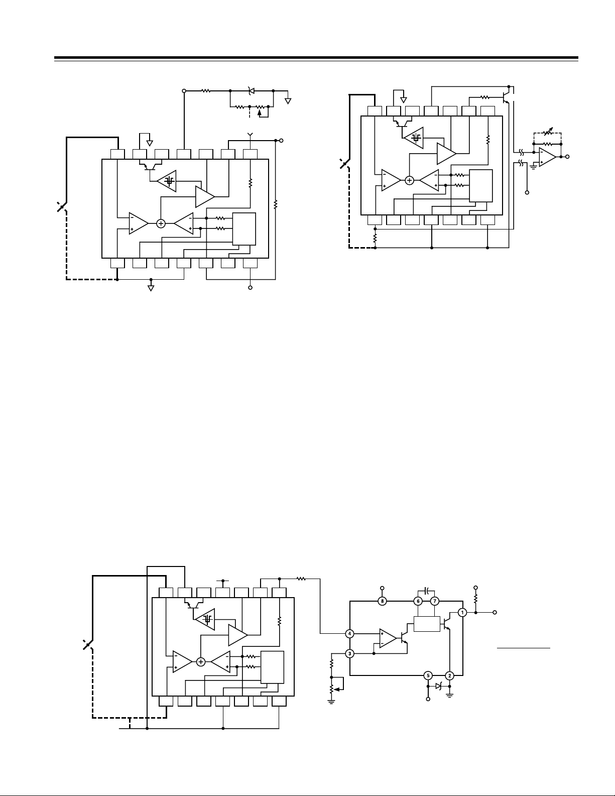
OPTIMIZING PERFORMANCE
Cold Junction Errors
Optimal performance from the AD594/AD595 is
achieved when the thermocouple cold junction and the
device are at thermal equilibrium. Avoid placing heat
generating devices or components near the AD594/
AD595 as this may produce cold junction related errors.
The ambient temperature range for the AD594/AD595 is
specified from 0°C to +50°C, and its cold junction com-
pensation voltage is matched to the best straight line fit
of the thermocouple’s output within this range. Operation outside this range will result in additional error.
Table II shows the maximum calculated errors at various
ambient temperatures.
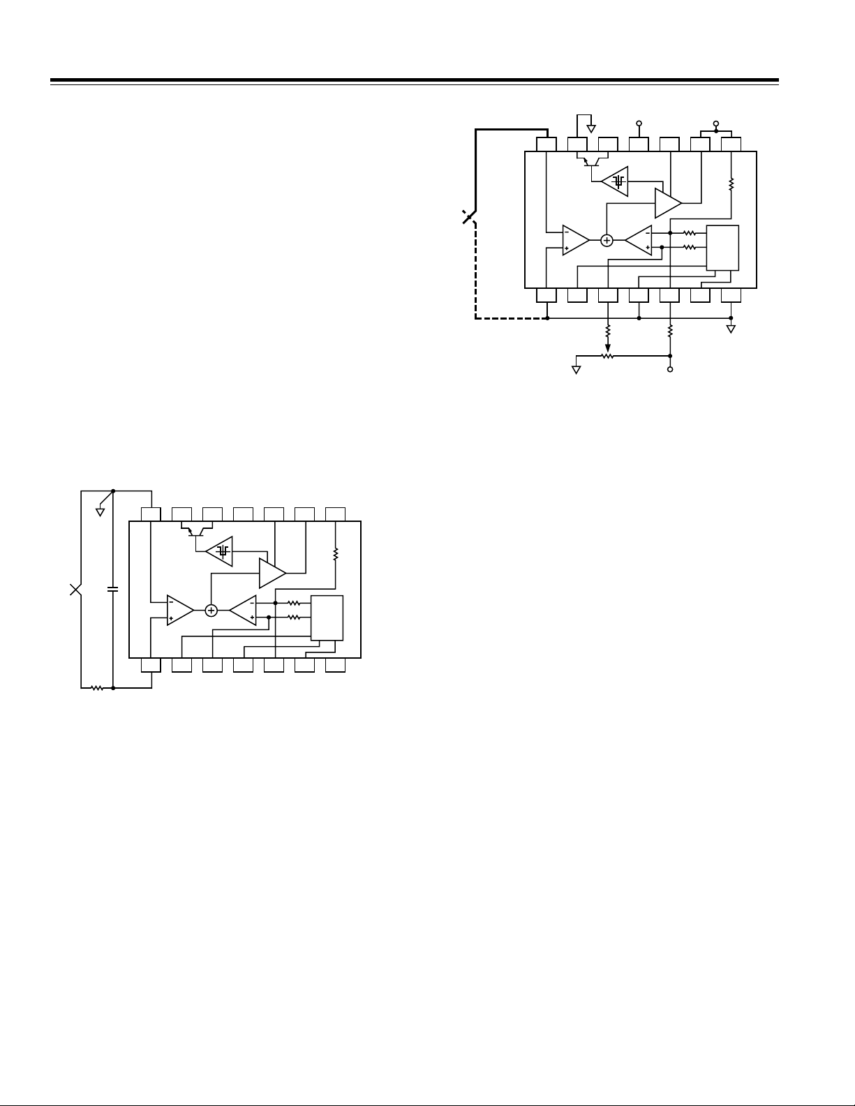
Circuit Board Layout
The circuit board layout shown in Figure 3 (with the optional calibration resistors) achieves thermal equilibrium between the cold junction and the AD594/AD595.
The package temperature and circuit board are thermally contacted in the copper printed circuit board
tracks under Pins 1 and 14. The reference junction is now
composed of a copper-constantan (or copper-alumel)
connection and copper-iron (or copper-chromel) connection in thermal equilibrium with the IC.
(CHROMEL)
+C+T
IRON
+IN –IN
1
CONSTANTAN
(ALUMEL)
14
–ALM
+ALM
Soldering
Proper soldering techniques and surface preparation
are necessary to bond the thermocouple to the PC
tracks. Clean the thermocouple wire to remove oxidation before soldering. Noncorrosive rosin flux may be
used with the following solders: 95% tin-5% antimony,
95% tin-5% silver, or 90% tin-10% lead.
Bias Current Return
The input instrumentation amplifier of the AD594/AD595
requires a return path for its input bias current and may
not be left “floating.” If the thermocouple measuring
junction is electrically isolated, then Pin 1 of the IC
should be connected to Pin 4, the power supply common. In some applications, tying the thermocouple directly to common is not possible. A resistor from Pin 1 to
common will satisfy the bias current return path but will,
however, generate an additional input offset voltage
due to the 100 nA bias current flowing through it. If the
thermocouple must be grounded at the measuring junction or if a small common mode potential is present, do
not make the connection between Pins 1 and 4.
Noise Suppression
When detecting a low level output voltage from a thermocouple, noise reduction is a prime concern. Whether
internally generated or induced by radiation from a
source, noise becomes one of the limiting factors of dynamic range and resolution. Solving noise problems involves eliminating the source and/or shielding. The
latter is more effective when the source cannot be controlled or identified.
Noise may be injected into the AD594/AD595 input amplifier when using a long length of thermocouple. To
determine if this noise path is the culprit, disconnect the
COMMON
AD594
AD595
–T – C V– V
Figure 3. PC Board Layout
OUT
87
COMP
V+
thermocouple from the AD594/AD595 and tie Pins 1 and
14 to Pin 4. The output voltage at Pin 9 of the AD594/
AD595 will now indicate ambient temperature (250 mV
at +25°C). If the noise at the output (Pin 9) disappears,
then shielding on the input is required. Shielded thermocouple wire with the shield connected to Pin 4 of the
IC will provide effective noise suppression. If the output
–3–
Page 4
AN-369
still exhibits noise, it may be entering via the power supply. Proper power supply bypassing and decoupling will
alleviate this condition.
Filtering the thermocouple input will attenuate the noise
before amplification. Figure 4 illustrates an effective input filter consisting of a resistor in series with Pin 1 and
a capacitor from this pin to ground. An offset voltage
will result due to the input bias current flowing through
the resistor. Since the input bias current for the inverting
input (Pin 14) varies with input voltage, any resistance in
series with this input would produce an input dependent
offset voltage. Therefore, it is highly recommended to connect this pin directly to common. In addition, the capacitor
across the input terminals increases the response time for
the alarm circuit in the event of a broken thermocouple.
Adding capacitance to the frequency compensation pin
(Pin 10) rolls off the bandwidth of the AD594/AD595 output
amplifier thus limiting noise. Without compensation, the
3 dB bandwidth is approximately 10 kHz. A 0.1 µF capacitor
connected between Pins 10 and 11 reduces the 3 dB point
to 120 Hz. This technique, however, is only useful if the
noise does not drive the input stage into saturation.
V
+TC
O
ICE
POINT
COMP.
FB
–TC
–IN –ALM +ALM V+ COMP
14 13
AD594/
AD595
G
1234567
+IN +C +T COM V––T –C
11 10 9 8
12
OVER-
LOAD
DETECT
+A
G
Figure 4. Input Filtering
TRIMMING CALIBRATION ERROR
The AD594/AD595, available in two performance grades,
is factory trimmed to achieve a maximum calibration error of 1°C or 3°C depending on grade. For most applications, this range of error is acceptable; however, by
adding the optional trim circuit shown in Figure 5, this
error may be nulled. A negative offset of approximately
3°C is injected into Pin 5. The trimming potentiometer
provides a balancing current into Pin 3 thus nulling any
calibration error.
+TC
V
OUT
ICE
POINT
COMP.
–TC
CONSTANTAN
(ALUMEL)
IRON
(CHROMEL)
+15V
14 13
AD594/
AD595
G
1234567
8MV 15MV
11 10 9 8
12
OVER-
LOAD
DETECT
+A
G
+T –T
R
CAL
100kV
+15V
Figure 5. Optional Calibration
OFFSETTING AND GAIN CHANGE
The AD594/AD595 is designed to produce a 0 V output at
0°C with a nominal gain of 10 mV/°C, but other ranges
are readily possible. The zero output temperature may
be changed by applying an offset voltage to Pin 8. The
magnitude of this voltage is calculated using the equations for the AD594/AD595 output voltage for a given
thermocouple temperature. Gain changes are easily accommodated by adding series resistance to increase
gain or by paralleling the nominal 47 kΩ feedback resis-
tor for gain reduction. The following method illustrates
this principle.
1. Select a temperature range T1–T2.
2. Based on this range, determine an output sensitivity
(mV/°C) that limits the maximum output excursions
from (–V
to (+V
+ 2.5) to (+VS – 2) for dual supplies or from 0
S
– 2) for single supply operation.
S
3. Calculate the average thermocouple sensitivity over
the selected temperature range: (VT1–VT2)/(T1–T2).
4. Divide the desired output sensitivity (mV/°C) by the
average thermocouple sensitivity (mV/°C). This yields
the new gain (G) for the AD594/AD595.
5. Measure the actual feedback resistance between Pins
8 and 5, R
.
FB
6. RIN = RFB/193.4 –1 where RFB is the measured feedback
resistance. NOTE: Use 247.3 for an AD595 instead of
193.4.
7. The new feedback resistance, R
–4–
= (G × 1)(R
EXT
).
IN
Page 5
AN-369
14 13
12
11 10 9 8
1234567
AD594/
AD595
G
+A
OVER-
LOAD
DETECT
ICE
POINT
COMP.
–TC
+TC
G
–V
S
(0V TO –15V)
CONSTANTAN
(ALUMEL)
IRON
(CHROMEL)
(OPTIONAL)
R
COMP
OSC/
DRIVER
AD654
C
T
R1
R2
CR1
+V
LOGIC
R
PU
F
OUT
+V
S
(+5V TO –VS + 30)
F
OUT
=
V
IN
(10V) (R1 + R2) C
T
+5V
COMMON
IN704A
4.1V
1kV
464V
TEMPERATURE
OFFSET VOLTAGE
FDBK
ICE
POINT
COMP.
+TC
–TC
–5V
V
R
EXT
CONSTANTAN
(ALUMEL)
IRON
(CHROMEL)
+5V
182V
14 13
AD594/
AD595
G
1234567
11 10 9 8
12
OVER-
LOAD
DETECT
+A
G
R
Figure 6. Offsetting and Gain Change
CURRENT MODE TRANSMISSION
In many applications, the AD594/AD595 may be located
in a noisy, remote location with its output driving a long
length of cable. Under these demanding conditions, current transmission offers better noise immunity and
eliminates errors due to cable resistance. The circuit
shown in Figure 7 converts the AD594/AD595 output to a
current and then converts it back to a voltage at the control point. The feedback voltage at Pin 9 forces the voltage across R
With the values shown for R
to equal the thermocouple voltage.
SENSE
, this produces a cur-
SENSE
rent output scale factor of 10 µA/°C. Note that the AD594/
AD595 quiescent current flows through the sense resistor, thus limiting the minimum measured temperature
to 16°C. The AD711 op amp converts this current back to
a nominal 10 mV/°C at the control point. Total error is
based upon the AD594/AD595 calibration error and the
match between the sense resistor and the 1 kΩ current
to voltage conversion resistor at the control point.
OUT
56kV
ICE
POINT
COMP.
–10mA/8C
2N2222
(OPTIONAL GAIN TRIM)
–TC
–15V
100kV
1kV
AD711
V
OUT
10mV/8C
CONSTANTAN
(ALUMEL)
14 13
1234567
IRON
(CHROMEL)
12
AD594/
AD595
G
R
SETUP
5.11V (4.02V)
11 10 9 8
OVER-
LOAD
DETECT
+A
G
+TC
Figure 7. Current-Mode Transmission
TEMPERATURE-TO-FREQUENCY CONVERSION
A digital output format may be produced by converting
the AD594/AD595 voltage output to a frequency. This
format not only affords noise immunity over long transmission paths but also provides information which may
be directly interfaced to a computer. A low cost
voltage-to-frequency converter, the AD654, converts the
10 mV/°C voltage output to a TTL compatible square
wave output. As shown in Figure 8, the entire system is
powered from a single 5 V supply and provides tem-
perature measurements from 0°C to +300°C. Higher
thermocouple temperatures will require a higher power
supply voltage to maintain a maximum AD594/AD595
output swing of 2.5 V below the supply. The AD594/
AD595 output voltage is connected to the AD654 input
through a series resistor to produce a 0 mA to 1 mA
full-scale current. Capacitor C
determines the full-scale
T
output frequency with a maximum usable frequency of
500 kHz resulting in 0.4% nonlinearity. Other temperature ranges and output frequencies are achievable. Refer to the AD654 data sheet for additional information.
=
Figure 8. Temperature-to-Frequency Conversion
–5–
Page 6
AN-369
FAHRENHEIT OUTPUT
The AD594/AD595 may be configured to produce a voltage proportional to the temperature on a Fahrenheit
scale. Conversion of temperature from a Celsius to Fahrenheit scale involves multiplying degrees Celsius by 9/5
and adding a 32 degree offset. The offset is produced by
injecting a 200 nA/°C current into Pin 3 while increasing
the feedback resistor to accommodate the gain of 9/5.
Output calibration is as follows:
1. With the thermocouple disconnected, apply a 10 mV
p-p, 100 Hz ac signal to Pins 1 and 14.
2. Adjust R
for a p-p output at Pin 9 of 3.481 V
GAIN
(AD594) or 4.451 V (AD595).
3. With the thermocouple connected and measuring
0°C, adjust R
until the output at Pin 9 reads
OFFSET
320 mV.
The ideal transfer function based on a Fahrenheit output
is:
AD594 Output = (Type J Voltage + 919 µV) × 348.12
AD595 Output = (Type K Voltage + 719 µV) × 445.14
This yields a higher output voltage swing over the useful
range of the thermocouple therefore, requiring a higher
power supply voltage to maintain a maximum output
voltage 2.5 V below the supply.
R
R
GAIN
2kV
9.1kV
OFFSET
2kV
5kV
598kV
CONSTANTAN
(ALUMEL)
IRON
(CHROMEL)
+20V
14 13
11 10 9 8
12
OVER-
LOAD
DETECT
AD594/
AD595
G
1234567
G
10mV/8F
+A
+TC
AD680
ICE
POINT
COMP.
7.5kV
–TC
–5V
Figure 9. Fahrenheit Output
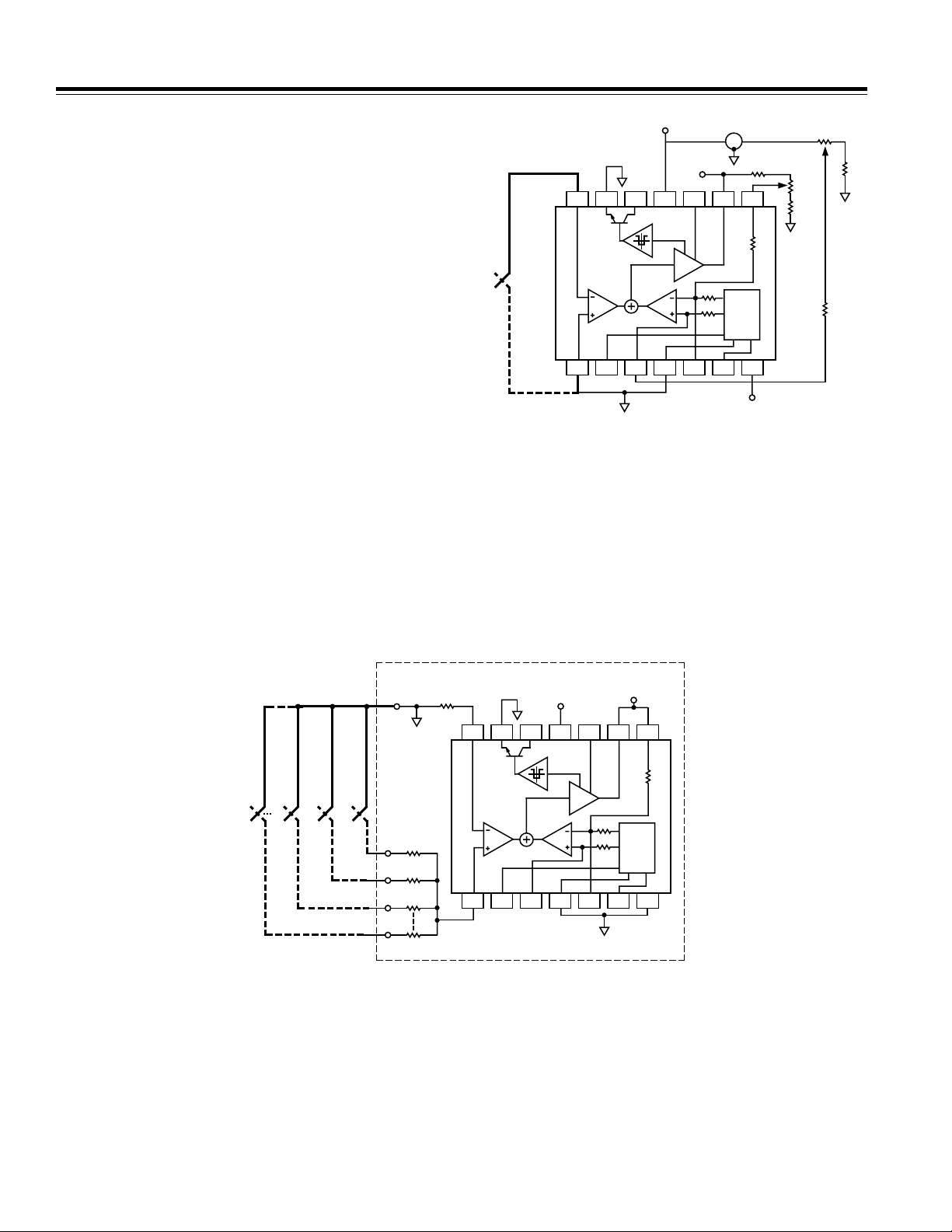
AVERAGE TEMPERATURE
By connecting a number of thermocouples in parallel to
the AD594/AD595 input, an average junction temperature
will be measured. As shown in Figure 10, a 300 Ω resistor
is placed in series with one side of each thermocouple to
limit the current circulating between the thermocouple
branches. Based on a thermocouple temperature that is
either higher or lower than the mean, a positive or negative voltage drop will be developed.
V
AVE
CONSTANTAN
(ALUMEL)
Cu
(R/N)V
14 13
+5V
11 10 9 8
12
OVER-
LOAD
DETECT
AD594/
e
3
N
2
IRON
(CHROMEL)
1
R
Cu
300V
R
Cu
300V
R
Cu
300V
Cu
R
300V
e
e
e
AD595
G
1234567
ISOTHERMAL
REGION
G
(T1, T2, T3 ... T
+A
+TC
OUT
ICE
POINT
COMP.
–TC
)
N
Figure 10. Measuring Average Temperature
–6–
Page 7
AN-369
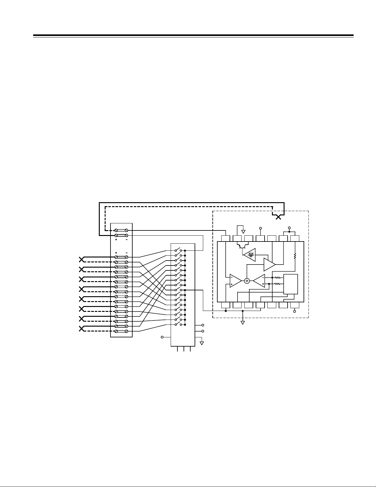
MULTIPLEXED THERMOCOUPLES
Multiple thermocouples may be connected to a single
AD595/AD595 via an external CMOS analog multiplexer
such as the ADG507A. For proper operation, all interconnects between the thermocouples, multiplexer and
AD594/AD595 inputs are copper and are held in thermal
equilibrium by an isothermal block. As shown in Figure
11, a thermocouple is mounted to measure the IC temperature as well as to cancel the reference junction voltage at the isothermal block. With the multiplexer
enabled, the Constantan (Alumel)—Copper junction
formed by the thermocouple connection at the isothermal block is in series with a Copper—Constantan
(Alumel) junction formed by the reference thermocouple connection.
This series combination contributes equal but opposite voltages since the block is isothermal. Under this
condition, the AD594/AD595 internal cold junction
Cu
Cu
V
2
+5V
19
20
21
22
23
24
25
26
11
10
9
8
7
6
5
4
18
EN
ADG507A
A
CONSTANTAN
(ALUMEL)
IRON
(CHROMEL)
V
1
ISOTHERMAL
BLOCK
Cu
Cu
Cu
Cu
Cu
Cu
Cu
Cu
Cu
Cu
Cu
Cu
Cu
Cu
Cu
Cu
CONSTANTAN
(ALUMEL)
IRON
(CHROMEL)
28
2
1
27
12
0A1A2
151617
compensation now compensates for the reference junc-
tion at the IC which must remain between 0°C and
+50°C. Note however, that the isothermal block may be
at any convenient temperature or location. Unused multiplexer inputs should be connected to common to minimize stray signal pickup. To prevent the AD594/AD595
inputs from “floating” resulting in output saturation, the
multiplexer is permanently enabled by connecting its
enable input to +5 V.
REFERENCES
1. Sheingold, Dan, ed.
Transducer Interface Handbook,
Analog Devices, 1980.
2.
1992 Amplifier Applications Guide,
Analog Devices,
Pub. No. G1646–10–4/92.
3. American Society for Testing and Materials,
Manual
On The Use Of Thermocouples In Temperature Measurement,
+15V
–15V
ASTM PCN 04-470020-40.
REFERENCE
JUNCTION
+15V
13
14
AD594/
AD595
G
1234567
11 10 9 8
12
OVER-
LOAD
DETECT
+A
G
ISOTHERMAL
REGION
+TC
V
OUT
ICE
POINT
COMP.
–15V
–TC
E1796a–0–7/98
Figure 11. Multiplexed Inputs
–7–
PRINTED IN U.S.A.
 Loading...