ANALOG DEVICES ADXRS453 Service Manual
High Performance,
V
Data Sheet
FEATURES
Complete rate gyroscope on a single chip
±300°/sec angular rate sensing
Ultrahigh vibration rejection: 0.01°/sec/g
Excellent 16°/hour null bias stability
Internal temperature compensation
2000 g powered shock survivability
SPI digital output with 16-bit data-word
Low noise and low power
3.3 V to 5 V operation
−40°C to +105°C operation
Ultrasmall, light, and RoHS compliant
Two package options
Low cost SOIC_CAV package for yaw rate (z-axis) response
Innovative ceramic vertical mount package (LCC_V) for
pitch and roll response
APPLICATIONS
Rotation sensing in high vibration environments
Rotation sensing for industrial and instrumentation
applications
High performance platform stabilization
Digital Output Gyroscope
ADXRS453
GENERAL DESCRIPTION
The ADXRS453 is an angular rate sensor (gyroscope) intended
for industrial, instrumentation, and stabilization applications in
high vibration environments. An advanced, differential, quad
sensor design rejects the influence of linear acceleration, enabling
the ADXRS453 to offer high accuracy rate sensing in harsh
environments where shock and vibration are present.
The ADXRS453 uses an internal, continuous self-test architecture. The integrity of the electromechanical system is checked by
applying a high frequency electrostatic force to the sense structure
to generate a rate signal that can be differentiated from the baseband rate data and internally analyzed.
The ADXRS453 is capable of sensing an angular rate of up to
±300°/sec. Angular rate data is presented as a 16-bit word that
is part of a 32-bit SPI message.
The ADXRS453 is available in a 16-lead plastic cavity SOIC
(SOIC_CAV) and an SMT-compatible vertical mount package
(LCC_V), and is capable of operating across a wide voltage
range (3.3 V to 5 V).
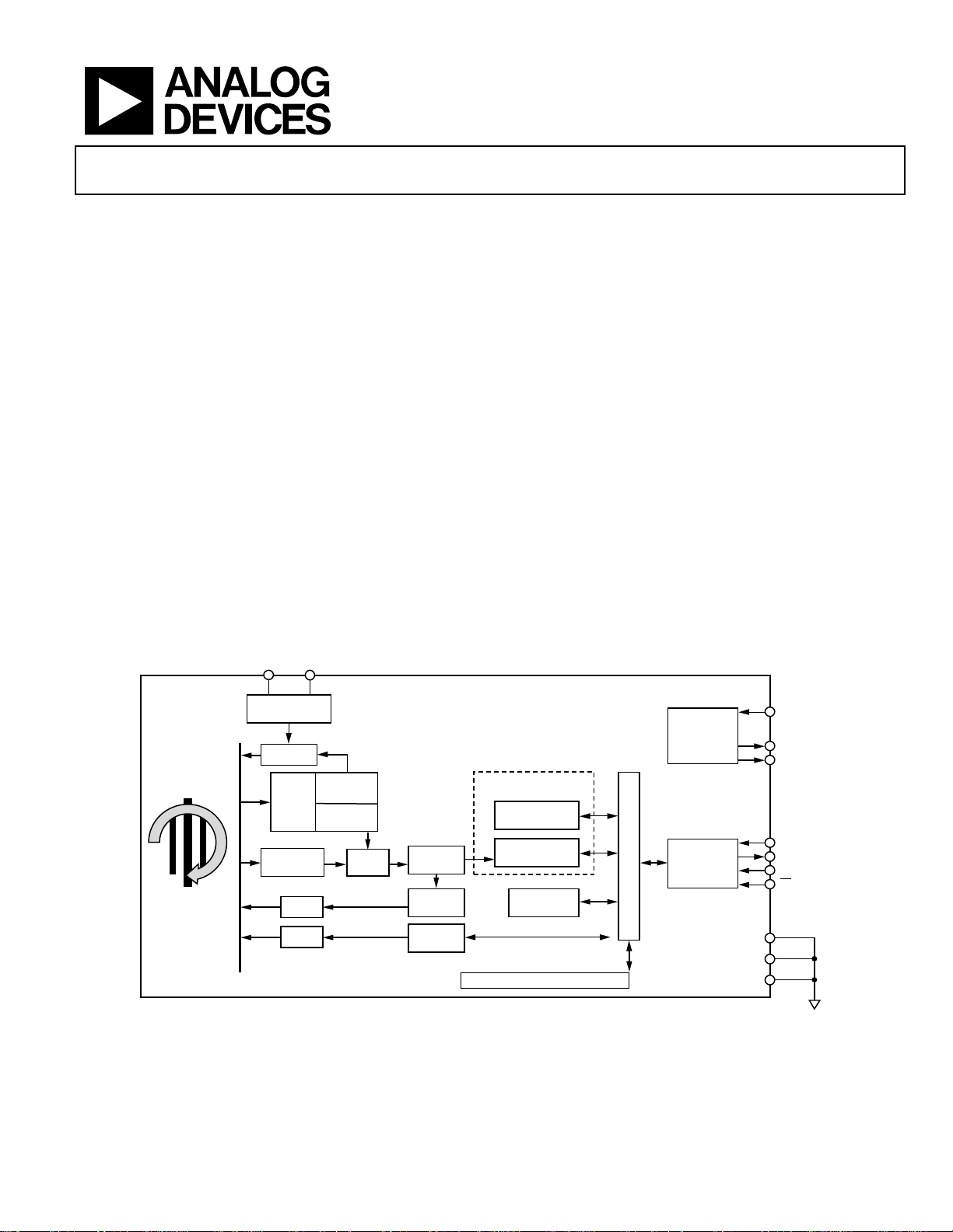
FUNCTIONAL BLOCK DIAGRAM
CP5
HIGH VO LTAG E
GENERATION
Z-AXIS ANGULAR
RATE SENSOR
HV DRIVE
PHASE-
LOCKED
LOOP
BAND-PASS
FILTER
Q DAQ
P DAQ
X
CLOCK
DIVIDER
AMPLITUDE
DETECT
12-BIT
ADC
DEMOD
Q FILTER
SELF-TEST
CONTROL
ADXRS453
ARITHMETIC
LOGIC UNIT
DECIMATION
TEMPERATURE
CALIBRATIO N
Figure 1.
FILTER
FAULT
DETECT ION
EEPROM
REGISTERS/MEMORY
LDO
REGULATOR
SPI
INTERFACE
P
DD
DV
DD
AV
DD
MOSI
MISO
SCLK
CS
DV
SS
P
SS
AV
SS
09155-001
Rev. B
Information furnished by Analog Devices is believed to be accurate and reliable. However, no
responsibility is assumed by Analog Devices for its use, nor for any infringements of patents or other
rights of third parties that may result from its use. Specifications subject to change without notice. No
license is granted by implication or otherwise under any patent or patent rights of Analog Devices.
Trademarks and registered trademarks are the property of their respective owners.
One Technology Way, P.O. Box 9106, Norwood, MA 02062-9106, U.S.A.
Tel: 781.329.4700 www.analog.com
Fax: 781.461.3113 ©2011 Analog Devices, Inc. All rights reserved.

ADXRS453 Data Sheet
TABLE OF CONTENTS
Features .............................................................................................. 1
Applications ....................................................................................... 1
General Description ......................................................................... 1
Functional Block Diagram .............................................................. 1
Revision History ............................................................................... 2
Specifications ..................................................................................... 3
Absolute Maximum Ratings ............................................................ 4
Thermal Resistance ...................................................................... 4
Rate Sensitive Axis ....................................................................... 4
ESD Caution .................................................................................. 4
Pin Configurations and Function Descriptions ........................... 5
Typical Performance Characteristics ............................................. 7
Theory of Operation ........................................................................ 9
Continuous Self-Test .................................................................... 9
Mechanical Performance ............................................................... 10
Noise Performance ......................................................................... 11
Applications Information .............................................................. 12
Calibrated Performance ............................................................. 12
Mechanical Considerations for Mounting .............................. 12
Application Circuits ................................................................... 12
ADXRS453 Signal Chain Timing ............................................. 13
SPI Communication Protocol ....................................................... 14
Command/Response ................................................................. 14
Device Data Latching ................................................................. 15
SPI Timing Characteristics ....................................................... 16
Command/Response Bit Definitions ....................................... 17
Fault Register Bit Definitions ................................................... 18
Recommended Start-Up Sequence with CHK Bit
Assertion ...................................................................................... 20
Rate Data Format ............................................................................ 21
Memory Map and Registers .......................................................... 22
Memory Map .............................................................................. 22
Memory Register Definitions ................................................... 23
Package Orientation and Layout Information ............................ 25
Solder Profile............................................................................... 26
Package Marking Codes ............................................................ 27
Outline Dimensions ....................................................................... 28
Ordering Guide .......................................................................... 29
REVISION HISTORY
12/11—Rev. A to Rev. B
Changes to Features Section............................................................ 1
Changes to Rate Sensitive Axis Section ......................................... 4
Deleted Endnote 1, Table 3 .............................................................. 4
Deleted Figure 5; Renumbered Sequentially ................................. 6
Changes to Figure 4 .......................................................................... 6
Changes to Figure 32 ...................................................................... 25
Deleted Figure 36 ............................................................................ 26
6/11—Rev. 0 to Rev. A
Changes to Bit 30 and Bit 31 in Table 9 ....................................... 14
Updated Outline Dimensions ....................................................... 29
Changes to Ordering Guide .......................................................... 30
1/11—Revision 0: Initial Version
Rev. B | Page 2 of 32

Data Sheet ADXRS453
SPECIFICATIONS
TA = T
Table 1.
Parameter Test Conditions/Comments Symbol Min Typ Max Unit
MEASUREMENT RANGE Full-scale range FSR ±300 ±400 °/sec
SENSITIVITY
NULL ACCURACY TA = 25°C ±0.4 °/sec
NOISE PERFORMANCE
T
LOW-PASS FILTER
SENSOR RESONANT FREQUENCY f0 13 15.5 19 kHz
SHOCK AND VIBRATION IMMUNITY
SELF-TEST
SPI COMMUNICATIONS
MEMORY REGISTERS
POWER SUPPLY
1
Maximum limit is guaranteed by Analog Devices, Inc., characterization.
2
Cross-axis sensitivity specification does not include effects due to device mounting on a printed circuit board (PCB).
3
Minimum and maximum limits are guaranteed by design.
MIN
to T
, PDD = 5 V, angular rate = 0°/sec, bandwidth = f0/200 (~77.5 Hz), ±1 g, continuous self-test on.
MAX
See
Figure 2
Nominal Sensitivity 80 LSB/°/sec
Sensitivity Tolerance TA = −40°C to +105°C −3 +3 %
Nonlinearity1 Best fit straight line 0.05 % FSR rms
Cross-Axis Sensitivity2 −3 +3 %
T
= −40°C to +105°C ±0.5 °/sec
A
Rate Noise Density TA = 25°C 0.015 °/sec/√Hz
= 105°C 0.023 °/sec/√Hz
A
Cutoff (−3 dB) Frequency f0/200 fLP 77.5 Hz
Group Delay3 f = 0 Hz tLP 3.25 4 4.75 ms
Sensitivity to Linear Acceleration DC to 5 kHz 0.01 °/sec/g
Vibration Rectification 0.0002 °/sec/g2
See the
Continuous Self-Test section
Magnitude 2559 LSB
Fault Register Threshold Compared to LOCSTx register data 2239 2879 LSB
Sensor Data Status Threshold Compared to LOCSTx register data 1279 3839 LSB
Frequency f0/32 fST 485 Hz
ST Low-Pass Filter
Cutoff (−3 dB) Frequency f0/8000 1.95 Hz
Group Delay3 52 64 76 ms
Clock Frequency 8.08 MHz
Voltage Input High
Voltage Input Low
MOSI,
MOSI,
CS
CS
, SCLK
, SCLK
0.85 × P
−0.3 P
PDD + 0.3 V
DD
× 0.15 V
DD
Voltage Output Low MISO, current = 3 mA 0.5 V
Voltage Output High MISO, current = −2 mA PDD − 0.5 V
Pull-Up Current
CS
, PDD = 3.3 V, CS = PDD × 0.15
CS
, PDD = 5 V, CS = PDD × 0.15
See the
Memory Register Definitions
60 200 μA
80 300 μA
section
Temperature Register
Value at 45°C 0 LSB
Scale Factor 5 LSB/°C
Quadrature, Self-Test, and Rate Registers
Scale Factor 80 LSB/°/sec
Supply Voltage PDD 3.15 5.25 V
Quiescent Supply Current IDD 6.0 8.0 mA
Turn-On Time Power-on to 0.5°/sec of final value 100 ms
Rev. B | Page 3 of 32
ADXRS453 Data Sheet
ABSOLUTE MAXIMUM RATINGS
Table 2.
Parameter Rating
Acceleration (Any Axis, 0.5 ms)
Unpowered 2000 g
Powered 2000 g
Supply Voltage (PDD) −0.3 V to +6.0 V
Output Short-Circuit Duration
Indefinite
(Any Pin to Ground)
Operating Temperature Range
LCC_V Package −55°C to +125°C
SOIC_CAV Package −40°C to +125°C
Storage Temperature Range
LCC_V Package −65°C to +150°C
SOIC_CAV Package −40°C to +150°C
Stresses above those listed under Absolute Maximum Ratings
may cause permanent damage to the device. This is a stress
rating only; functional operation of the device at these or any
other conditions above those indicated in the operational
section of this specification is not implied. Exposure to absolute
maximum rating conditions for extended periods may affect
device reliability.
THERMAL RESISTANCE
θJA is specified for the worst-case conditions, that is, for a device
soldered in a printed circuit board (PCB) for surface-mount
packages.
Table 3. Thermal Resistance
Package Type θJA θJC Unit
16-Lead SOIC_CAV (RG-16-1) 191.5 25 °C/W
14-Lead Ceramic LCC_V (EY-14-1) 185.5 23 °C/W
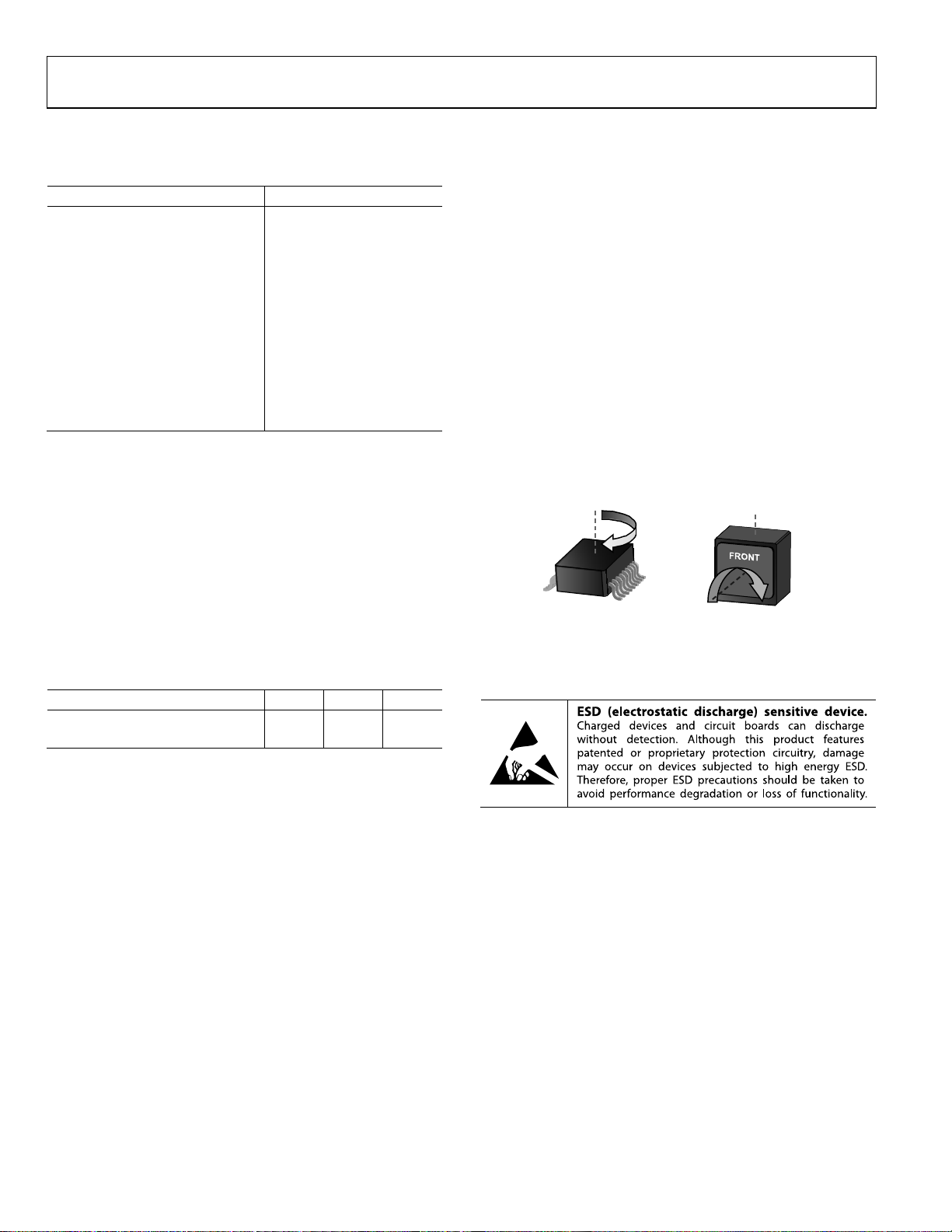
RATE SENSITIVE AXIS
The ADXRS453 is available in two package options.
The SOIC_CAV package is for applications that require
z-axis (yaw) rate sensing.
The LCC_V (vertical mount) package is for applications
that require x-axis or y-axis (pitch or roll) rate sensing.
The package has terminals on two faces. However, the terminals on the back are for internal evaluation only and should
not be used in the end application. The terminals on the
bottom of the package incorporate metallization bumps
that ensure a minimum solder thickness for improved solder
joint reliability. These bumps are not present on the back
terminals and, therefore, poor solder joint reliability can be
encountered if the back terminals are used in the end
application. For the outline dimensions of this package, see
Figure 38.
RATE
AXIS
+
16
RATE
SOIC PACKAGE
9
Figure 2. Rate Signal Increases with Clockwise Rotation
AXIS
Z-AXIS
+
LCC_V PACKAGE
09155-002
ESD CAUTION
Rev. B | Page 4 of 32
Data Sheet ADXRS453
PIN CONFIGURATIONS AND FUNCTION DESCRIPTIONS
DV
RSVD
RSVD
CS
MISO
P
P
DD
DD
SS
V
X
1
2
3
ADXRS453
4
TOP VIEW
(Not to Scale)
5
6
7
8
16
SCLK
15
MOSI
14
AV
DD
13
DV
SS
12
RSVD
11
AV
SS
10
RSVD
9
CP5
09155-003
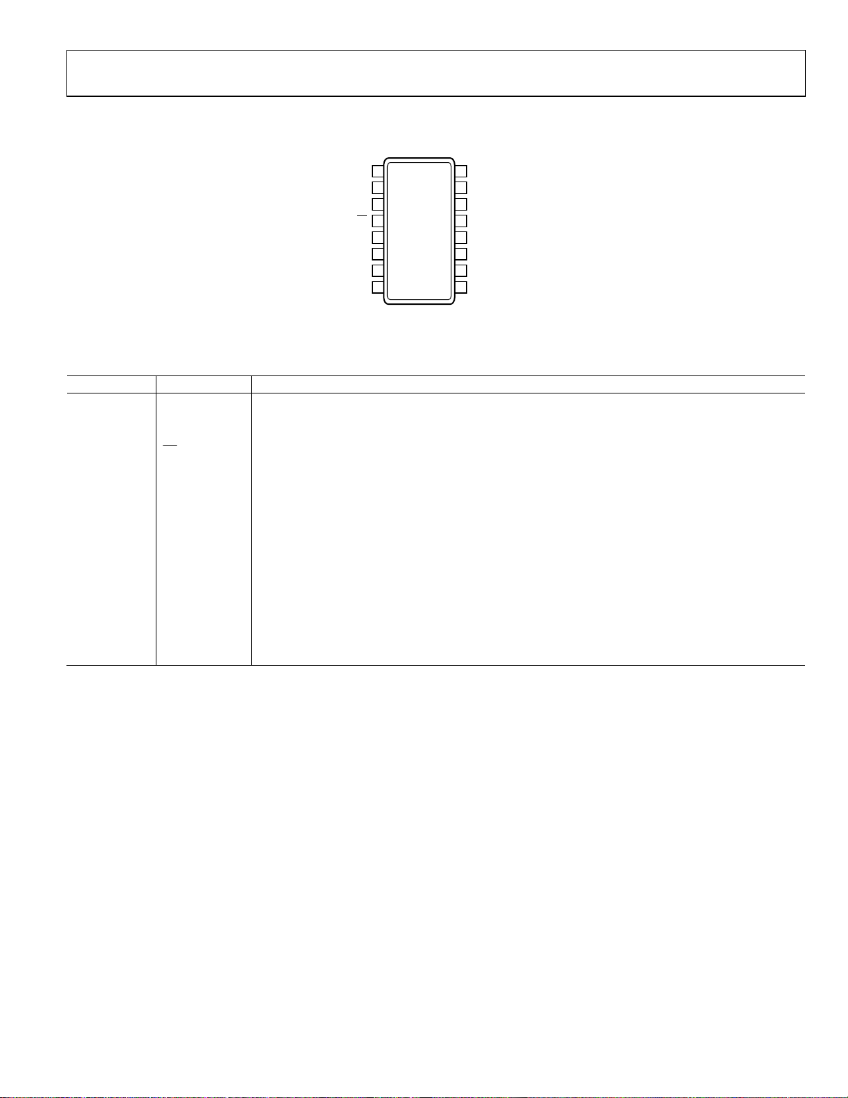
Figure 3. Pin Configuration, 16-Lead SOIC_CAV
Table 4. Pin Function Descriptions, 16-Lead SOIC_CAV
Pin No. Mnemonic Description
1 DVDD Digital Regulated Voltage. See Figure 25 for the application circuit diagram.
2 RSVD Reserved. This pin must be connected to DVSS.
3 RSVD Reserved. This pin must be connected to DVSS.
4
CS
Chip Select.
5 MISO Master In/Slave Out.
6 PDD Supply Voltage.
7 PSS Switching Regulator Ground.
8 VX High Voltage Switching Node. See Figure 25 for the application circuit diagram.
9 CP5 High Voltage Supply. See Figure 25 for the application circuit diagram.
10 RSVD Reserved. This pin must be connected to DVSS.
11 AVSS Analog Ground.
12 RSVD Reserved. This pin must be connected to DVSS.
13 DVSS Digital Signal Ground.
14 AVDD Analog Regulated Voltage. See Figure 25 for the application circuit diagram.
15 MOSI Master Out/Slave In.
16 SCLK SPI Clock.
Rev. B | Page 5 of 32

ADXRS453 Data Sheet
PDDPSSMOSI
14 13 12 11 10 9 8
1234567
SS
AV
NOTES
1. THE PACKAGE HAS T ERMINALS ON TWO FACES. HO WEVER, THE TERM INALS ON
THE BACK ARE FO R INTERNAL EVALUATI ON ONLY AND SHOULD NO T BE USED IN
THE END APPL ICATIO N. THE T ERMINALS ON THE BOT TOM O F THE PACKAG E
INCORPORAT E METAL LIZAT ION BUMPS THAT ENSURE A MINIMUM SOLDER
THICKNESS FOR IMPROVED SOLDER JOINT RELIABILITY. THESE BUMPS ARE
NOT PRESENT ON THE BACK TERMINAL S AND, THEREFORE, P OOR SOL DER
JOINT REL IABILI TY CAN BE ENCOUNT ERED IF TH E BACK TERMINALS ARE USED
IN THE END APPLICATI ON. FO R THE OUT LINE DI MENSIONS OF THI S PACKAGE,
SEE FIGURE 38.
DVSSCS
DD
DD
AV
MISO
DV
TOP VIEW
(Not to Scale)
SCLK
VXRSVD
CP5
RSVD
09155-004
Figure 4. Pin Configuration, 14-Terminal LCC_V
Table 5. Pin Function Descriptions, 14-Terminal LCC_V
Pin No. Mnemonic Description
1 AVSS Analog Ground.
2 AVDD Analog Regulated Voltage. See Figure 26 for the application circuit diagram.
3 MISO Master In/Slave Out.
4 DVDD Digital Regulated Voltage. See Figure 26 for the application circuit diagram.
5 SCLK SPI Clock.
6 CP5 High Voltage Supply. See Figure 26 for the application circuit diagram.
7 RSVD Reserved. This pin must be connected to DVSS.
8 RSVD Reserved. This pin must be connected to DVSS.
9 VX High Voltage Switching Node. See Figure 26 for the application circuit diagram.
10
CS
Chip Select.
11 DVSS Digital Signal Ground.
12 MOSI Master Out/Slave In.
13 PSS Switching Regulator Ground.
14 PDD Supply Voltage.
Rev. B | Page 6 of 32
Data Sheet ADXRS453
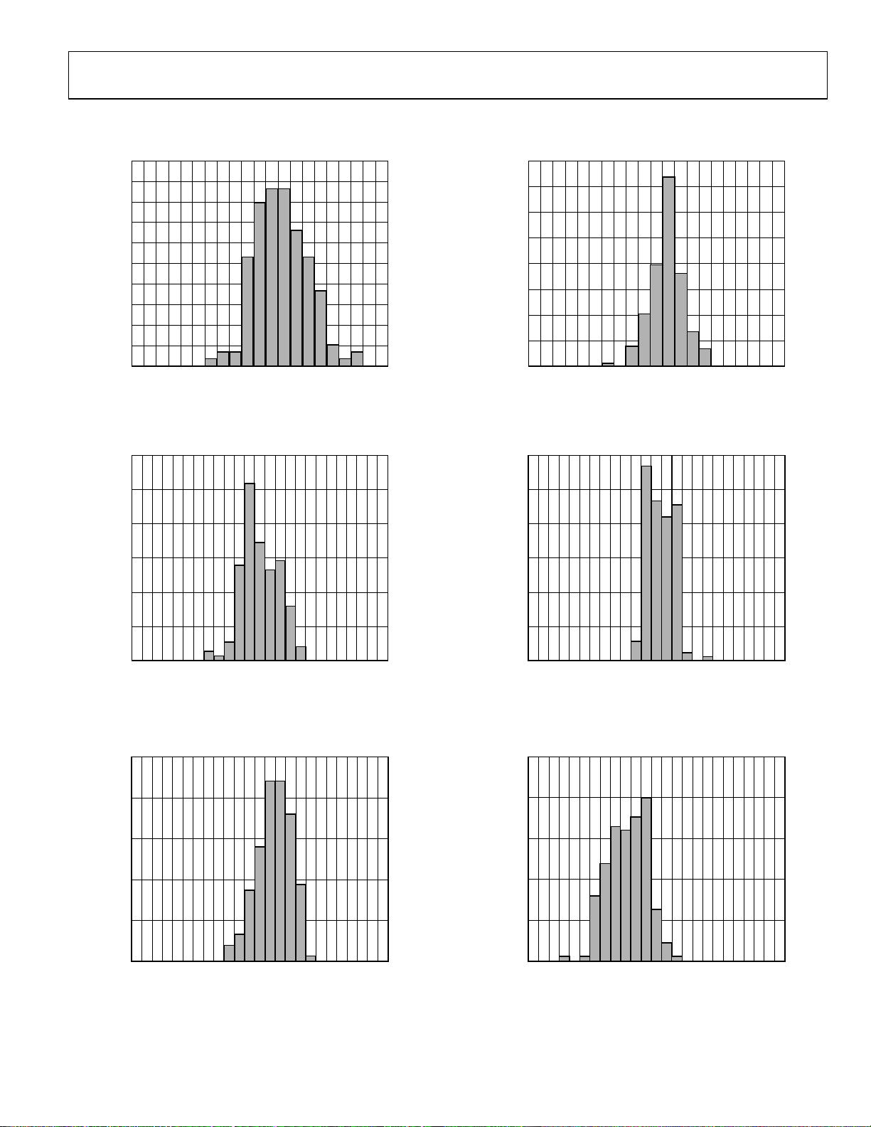
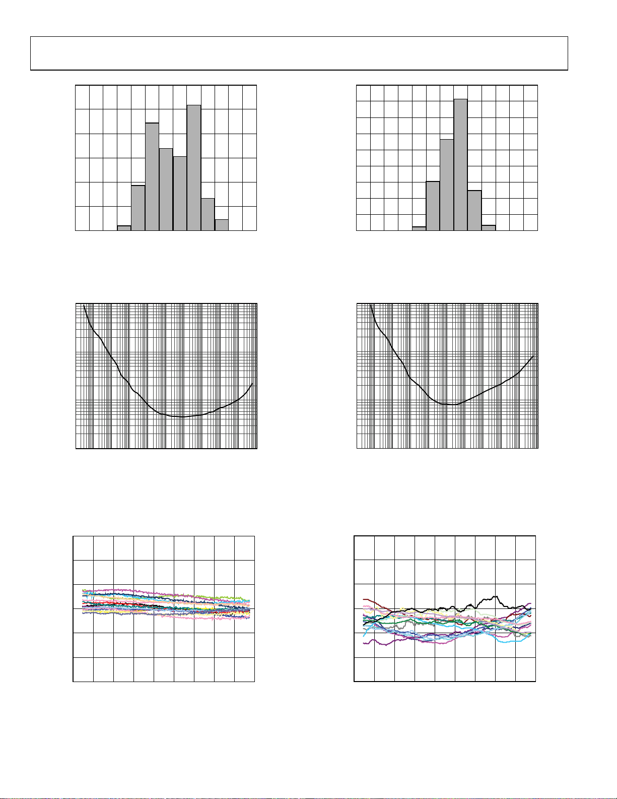
TYPICAL PERFORMANCE CHARACTERISTICS
20
18
16
14
12
10
8
6
4
PERCENT OF POPULATION (%)
2
0
–2.0 –1.6 –1.2 –0.8 –0.4 0 2.01.61.20.80.4
ERROR (°/sec)
Figure 5. SOIC_CAV Null Accuracy at 25°C
09155-006
40
35
30
25
20
15
10
PERCENT OF POPULATION (%)
5
0
–2.0 –1.6 –1.2 –0.8 –0.4 0 2.01.61.20.80.4
ERROR (°/sec)
Figure 8. LCC_V Null Accuracy at 25°C
09155-009
30
25
20
15
10
PERCENT OF POPUL ATION (%)
5
0
–2.5
–2.0
–3.0
–1.5
–1.0
–0.5
ERROR (°/sec)
0
Figure 6. SOIC_CAV Null Drift over Temperature
25
20
15
30
25
20
15
10
PERCENT OF POPUL ATION (%)
5
0
0.5
1.0
1.5
2.0
2.5
3.0
09155-007
–2.5
–2.0
–3.0
–1.5
–0.5
–1.0
ERROR (°/ sec)
0
1.5
1.0
0.5
3.0
2.5
2.0
09155-010
Figure 9. LCC_V Null Drift over Temperature
25
20
15
PERCENT OF POPULATION (%)
10
5
0
–0.030
–0.025
–0.020
–0.015
–0.010
–0.005
CHANGE IN SENSI TIVITY (%)
Figure 10. LCC_V Sensitivity Error at 25°C
0
0.030
0.025
0.020
0.015
0.010
0.005
09155-011
10
5
PERCENT OF POPULATIO N (%)
0
–3.0
–2.5
–2.0
–1.5
CHANGE IN SENSI TIVITY (%)
0
0.5
1.0
1.5
2.0
2.5
–1.0
–0.5
3.0
09155-008
Figure 7. SOIC_CAV Sensitivity Error at 25°C
Rev. B | Page 7 of 32
ADXRS453 Data Sheet
30
25
20
15
10
PERCENT OF POPULATION (%)
5
0
–3 –2 –1
0
ERROR (%)
Figure 11. SOIC_CAV Sensitivity Drift over Temperature
321
09155-012
45
40
35
30
25
20
15
10
PERCENT OF POPULAT ION (%)
5
0
–3 –2 –1
0
ERROR (%)
Figure 14. LCC_V Sensitivity Drift over Temperature
321
09155-015
ROOT ALL AN VARIANCE (°/ sec)
0.001
1
0.1
0.01
0.01
0.001
0.0001
0.00001
0.0000001
0.000001
AVERAGING TIME (Hours)
Figure 12. Typical Root Allan Variance at 40°C
3
2
1
1
0.1
0.01
ROOT ALL AN VARIANCE (°/ sec)
1
0.1
10
100
1000
09155-013
0.001
0.0000001
0.01
0.001
0.0001
0.00001
0.000001
AVERAGING TIME (Hours)
1
0.1
10
100
1000
09155-016
Figure 15. Typical Root Allan Variance at 105°C
3
2
1
0
–1
NULL OUTPUT (°/sec)
–2
–3
–50 –30 –10 10 30 50 70 90 110 130
TEMPERATURE (°C)
Figure 13. Null Output over Temperature, 16 Devices Soldered on PCB
09155-014
Rev. B | Page 8 of 32
0
ERROR (%)
–1
–2
–3
–50 –30 –10 10 30 50 70 90 110 130
TEMPERATURE (°C)
Figure 16. Sensitivity over Temperature, 16 Devices Soldered on PCB
09155-017
Data Sheet ADXRS453
THEORY OF OPERATION
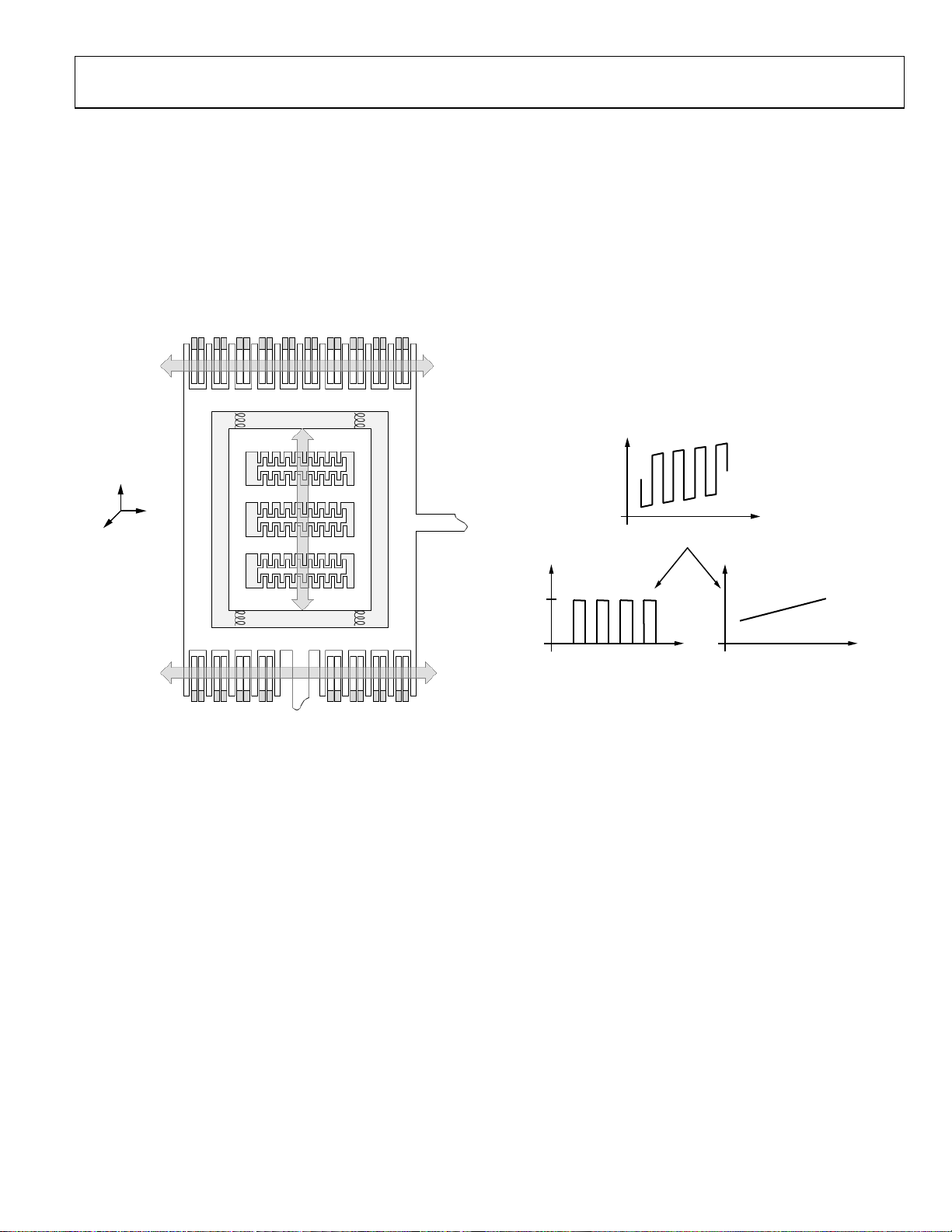
The ADXRS453 operates on the principle of a resonator gyroscope.
Figure 17 shows a simplified version of one of four polysilicon
sensing structures. Each sensing structure contains a dither frame
that is electrostatically driven to resonance. This produces the
necessary velocity element to produce a Coriolis force when the
device experiences angular rate. In the SOIC_CAV package, the
ADXRS453 is designed to sense a z-axis (yaw) angular rate; the
LCC_V vertical mount package orients the device such that it
can sense pitch or roll angular rate on the same PCB.
X
Y
Z
CONTINUOUS SELF-TEST
The ADXRS453 gyroscope implements a complete electromechanical self-test. An electrostatic force is applied to the
gyroscope frame, resulting in a deflection of the capacitive sense
fingers. This deflection is exactly equivalent to deflection that
occurs as a result of external rate input. The output from the
beam structure is processed by the same signal chain as a true
rate output signal, providing complete coverage of both the
electrical and mechanical components.
The electromechanical self-test is performed continuously
during operation at a rate higher than the output bandwidth of
the device. The self-test routine generates equivalent positive
and negative rate deflections. This information can then be
filtered with no overall effect on the demodulated rate output.
RATE SIGNAL WITH
CONTINUOUS SELF-T EST SIGNAL.
Figure 17. Simplified Gyroscope Sensing Structure
When the sensing structure is exposed to angular rate, the
resulting Coriolis force couples into an outer sense frame,
which contains movable fingers that are placed between fixed
pickoff fingers. This forms a capacitive pickoff structure that
senses Coriolis motion. The resulting signal is fed to a series of
gain and demodulation stages that produce the electrical rate
signal output. The quad sensor design rejects linear and angular
acceleration, including external g-forces and vibration. This is
achieved by mechanically coupling the four sensing structures
such that external g-forces appear as common-mode signals
that can be removed by the fully differential architecture
implemented in the ADXRS453.
The resonator requires 22.5 V (typical) for operation. Because
only 5 V is typically available in most applications, a switching
regulator is included on chip.
SELF-TEST AMPLITUDE.
INTERNALL Y COMPARED
TO THE SPECIFICATION
09155-018
TABLE LI MITS.
Figure 18. Continuous Self-Test Demodulation
LOW FREQUENCY RATE
INFORMAT ION.
The difference amplitude between the positive and negative
self-test deflections is filtered to f
/8000 (~1.95 Hz) and is
0
continuously monitored and compared to hard-coded self-test
limits. If the measured amplitude exceeds these limits (listed in
Table 1), one of two error conditions is asserted, depending on
the magnitude of the self-test error.
For less severe self-test error magnitudes, the CST bit of the
fault register is asserted. However, the status bits (ST[1:0])
in the sensor data response remain set to 01 for valid
sensor data.
For more severe self-test errors, the CST bit of the fault
register is asserted and the status bits (ST[1:0]) in the
sensor data response are set to 00 for invalid sensor data.
Table 1 lists the thresholds for both of these failure conditions.
If desired, the user can access the self-test information by issuing
a read command to the self-test memory register (Address 0x04).
See the SPI Communication Protocol section for more information about error reporting.
09155-019
Rev. B | Page 9 of 32
ADXRS453 Data Sheet
(
MECHANICAL PERFORMANCE
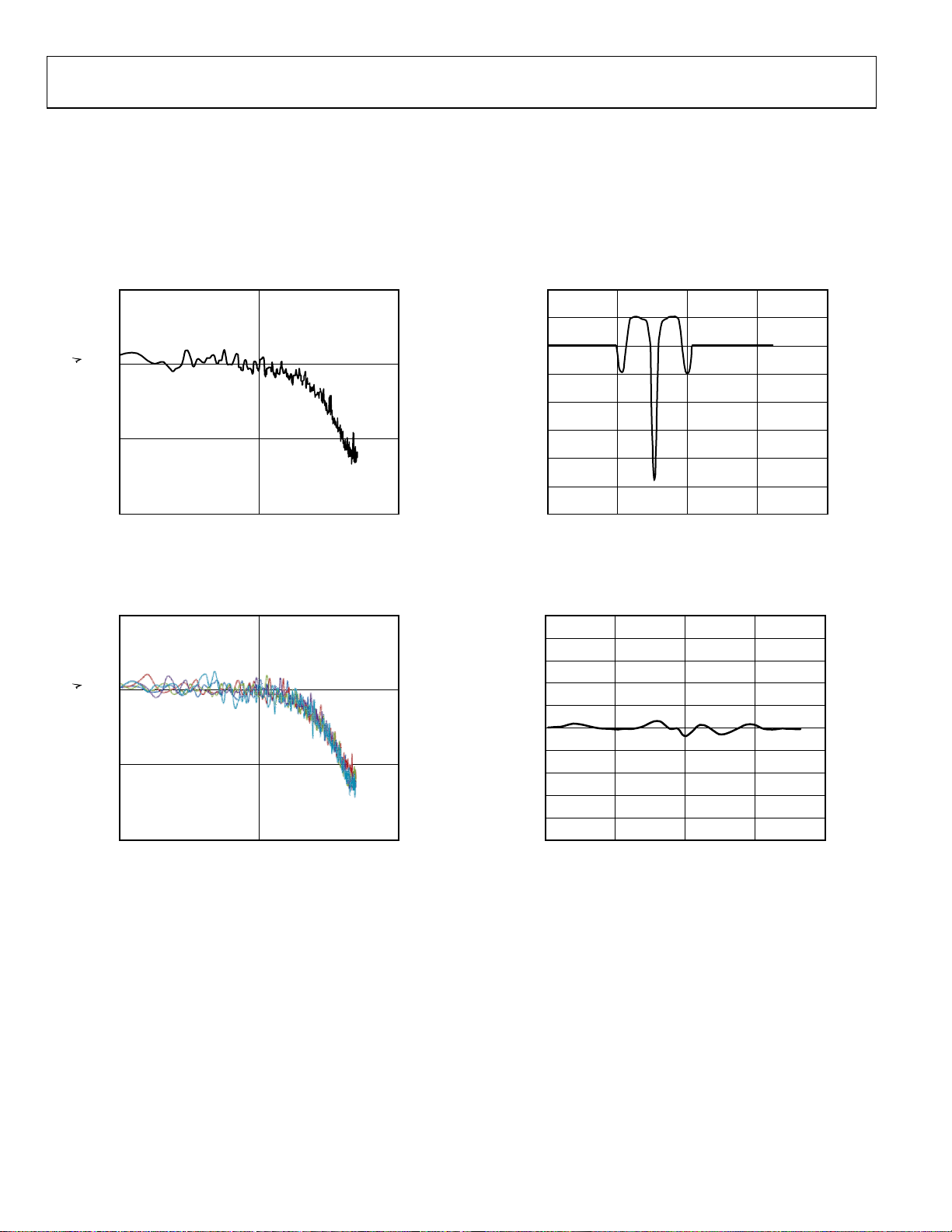
The ADXRS453 has excellent shock and vibration rejection.
Figure 19 shows the output noise response of the ADXRS453 in
a vibration free environment. Figure 20 shows the response of
the same device to 15 g rms random vibration (50 Hz to 5 kHz).
As shown in Figure 20, no frequencies are particularly sensitive
to vibration. Response to vibration in all axes is similar.
0.1
0.01
Shock response is also excellent, as shown in Figure 21 and
Figure 22. Figure 21 shows a 99 g input stimulus applied to
each axis, and Figure 22 shows the typical response to this
shock in each axis. Shock response of 0.01°/sec/g is apparent.
40
20
0
g)
–20
–40
0.001
GYRO OUTPUT (°/sec/ Hz)
0.0001
5 50 500
FREQUENCY (Hz)
Figure 19. ADXRS453 Output Noise Response with No Vibration Applied
0.1
0.01
0.001
GYRO OUTPUT (°/sec/ Hz)
0.0001
5 50 500
FREQUENCY (Hz)
Figure 20. ADXRS453 Output Noise Response with 15 g RMS Random
Vibration (50 Hz to 5 kHz) Applied
–60
INPUT STIMULUS
–80
–100
–120
00.100.05 0.15 0.20
09155-020
TIME (Seconds)
09155-022
Figure 21. 99 g Shock Input
10
8
6
4
2
0
–2
–4
GYRO OUTPUT (°/sec)
–6
–8
–10
00.100.05 0.15 0.20
09155-021
TIME (Seconds)
09155-023
Figure 22. Typical Output Response Due to 99 g Shock (see Figure 21)
Rev. B | Page 10 of 32
 Loading...