ANALOG DEVICES ADXL78 Service Manual

Single-Axis, High-g,
FEATURES
Complete acceleration measurement system on a single
monolithic IC
Available in ±35 g, ±50 g, or ±70 g output full-scale ranges
Full differential sensor and circuitry for high resistance
to EMI/RFI
Environmentally robust packaging
Complete mechanical and electrical self-test on
digital command
Output ratiometric to supply
Sensitive axes in the plane of the chip
High linearity (0.2% of full scale)
Frequency response down to dc
Low noise
Low power consumption (1.3 mA)
Tight sensitivity tolerance and 0 g offset capability
Largest available prefilter clipping headroom
400 Hz, 2-pole Bessel filter
Single-supply operation
Compatible with Sn/Pb and Pb-free solder processes
Qualified for automotive applications
®
iMEMS
Accelerometers
ADXL78
GENERAL DESCRIPTION
The ADXL78 is a low power, complete single-axis accelerometer
with signal conditioned voltage outputs that are on a single
monolithic IC. This product measures acceleration with a fullscale range of ±35 g, ±50 g, or ±70 g (minimum). It can also
measure both dynamic acceleration (vibration) and static
acceleration (gravity).
The ADXL78 is the fourth-generation surface micromachined
iMEMS® accelerometer from ADI with enhanced performance
and lower cost. Designed for use in front and side impact airbag
applications, this product also provides a complete costeffective solution useful for a wide variety of other applications.
The ADXL78 is temperature stable and accurate over the
automotive temperature range, with a self-test feature that fully
exercises all the mechanical and electrical elements of the
sensor with a digital signal applied to a single pin.
The ADXL78 is available in a 5 mm × 5 mm × 2 mm,
8-terminal ceramic LCC package.
APPLICATIONS
Vibration monitoring and control
Vehicle collision sensing
Shock detection
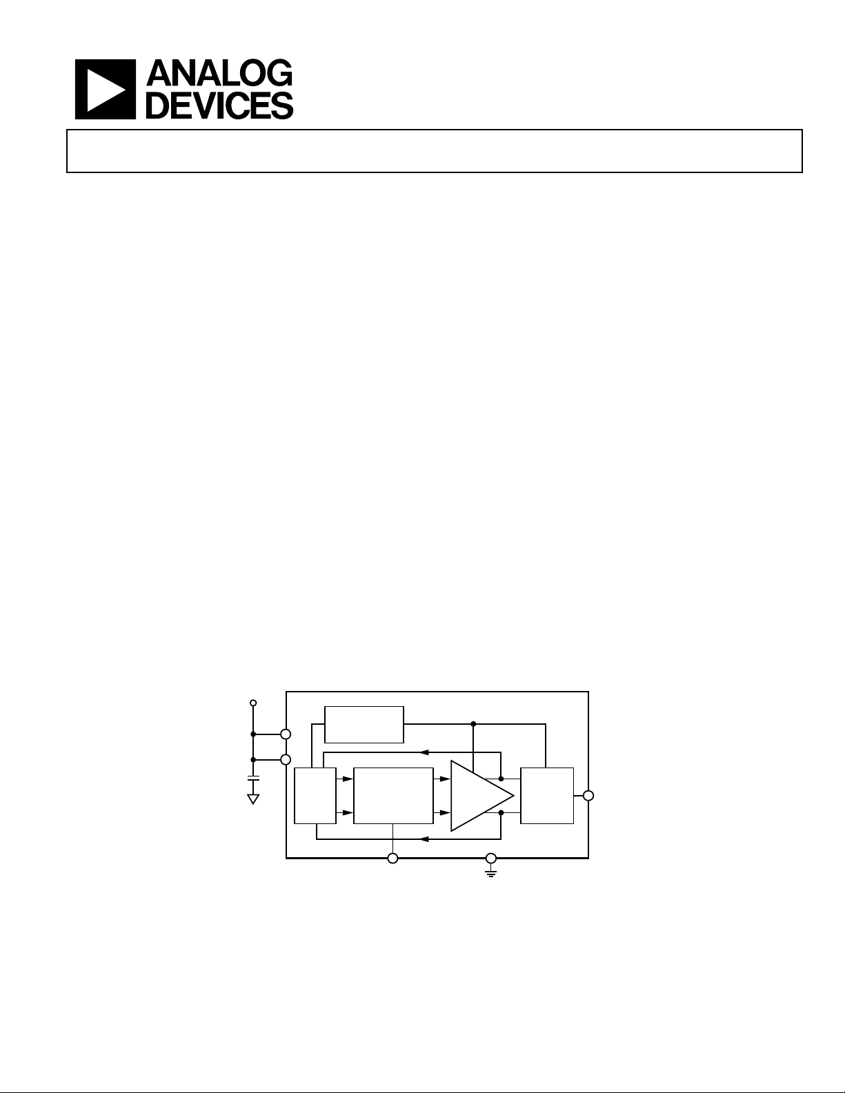
V
FUNCTIONAL BLOCK DIAGRAM
S
V
DD
V
DD2
EXC
TIMING
GENERATOR
DIFFERENTIAL
SENSOR
SELF-TEST
Figure 1.
DEMOD
AMP
ADXL78
400Hz
BESSEL
FILTER
X
OUT
05368-001
Rev. B
Information furnished by Analog Devices is believed to be accurate and reliable. However, no
responsibility is assumed by Analog Devices for its use, nor for any infringements of patents or other
rights of third parties that may result from its use. Specifications subject to change without notice. No
license is granted by implication or otherwise under any patent or patent rights of Analog Devices.
Trademarks and registered trademarks are the property of their respective owners.
One Technology Way, P.O. Box 9106, Norwood, MA 02062-9106, U.S.A.
Tel: 781.329.4700 www.analog.com
Fax: 781.461.3113 ©2010 Analog Devices, Inc. All rights reserved.

ADXL78
TABLE OF CONTENTS
Features .............................................................................................. 1
Applications ....................................................................................... 1
General Description ......................................................................... 1
Functional Block Diagram .............................................................. 1
Specifications ..................................................................................... 3
Absolute Maximum Ratings ............................................................ 4
ESD Caution .................................................................................. 4
Pin Configuration and Function Descriptions ............................. 5
Theory of Operation ........................................................................ 7
REVISION HISTORY
7/10—Rev. A to Rev. B
Updated Format ................................................................. Universal
Change to Features Section ............................................................. 1
Updated Outline Dimensions ......................................................... 9
Changes to Ordering Guide ............................................................ 9
Added Automotive Products Section ............................................ 9
5/05—Rev. 0 to Rev. A
Applications ........................................................................................8
Power Supply Decoupling ............................................................8
Self-Test ..........................................................................................8
Clock Frequency Supply Response .............................................8
Signal Distortion ...........................................................................8
Outline Dimensions ..........................................................................9
ADXL78 Ordering Guide .............................................................9
Automotive Products ....................................................................9
Rev. B | Page 2 of 12

ADXL78
SPECIFICATIONS1
At TA = −40°C to +105°C, 5.0 V dc ± 5%, acceleration = 0 g, unless otherwise noted.
Table 1.
Model No. AD22279 Model No. AD22280 Model No. AD22281
Parameter Conditions Min Typ Max Min Typ Max Min Typ Max Unit
SENSOR
Output Full-Scale Range I
≤ ±100 μA 37 55 70
OUT
Nonlinearity 0.2 2 0.2 2 0.2 2 %
Package Alignment Error 1 1 1 Degree
Cross-Axis Sensitivity −5 +5 −5 +5 −5 +5 %
Resonant Frequency 24 24 24 kHz
= 5 V, 100 Hz 52.25 55 57.75 36.1 38 39.9 25.65 27 28.35 mV/g
Sensitivity, Ratiometric
V
DD
(Over Temperature)
OFFSET
Zero-g Output Voltage
(Over Temperature)2
V
V
OUT
DD
= 5 V
− VDD/2,
−200 +200 −150 +150 −150 +150 mV
NOISE
Noise Density
10 Hz − 400 Hz,
1.1 3 1.4 3 1.8 3.5 mg/√Hz
5 V
Clock Noise 5 5 5 mV p-p
FREQUENCY RESPONSE 2-pole Bessel
−3 dB Frequency 360 400 440 360 400 440 360 400 440 Hz
−3 dB Frequency Drift
25°C to
or T
T
MIN
MAX
2 2 2 Hz
SELF-TEST
V
Output Change
= 5 V 440 550 660 304 380 456 216 270 324 mV
DD
(Cube vs. VDD)3
Logic Input High VDD = 5 V 3.5 3.5 3.5 V
Logic Input Low VDD = 5 V 1 1 1 V
Input Resistance
Pull-down
30 50 30 50 30 50 kΩ
resistor to GND
OUTPUT AMPLIFIER
Output Voltage Swing I
= ±400 μA 0.25 VDD − 0.25 0.25 VDD − 0.25 0.25 VDD − 0.25 V
OUT
Capacitive Load Drive 1000 1000 1000 pF
PREFILTER HEADROOM 280 400 560
CFSR @ 400 kHz 5 4 3 V/V
POWER SUPPLY (VDD) 4.75 5.25 4.75 5.25 4.75 5.25 V
Functional Range 3.5 6 3.5 6 3.5 6 V
Quiescent Supply Current VDD = 5 V 1.3 2 1.3 2 1.3 2 mA
TEMPERATURE RANGE −40 +105 −40 +105 −40 +105 °C
1
All minimum and maximum specifications are guaranteed. Typical specifications are not guaranteed.
2
Zero g output is ratiometric.
3
Self-test output at VDD = (Self-Test Output at 5 V) × (VDD/5 V)3.
g
g
Rev. B | Page 3 of 12

ADXL78
ABSOLUTE MAXIMUM RATINGS
Table 2.
Parameter Rating
Acceleration (Any Axis, Unpowered) 4000 g
Acceleration (Any Axis, Powered) 4000 g
VS −0.3 V to +7.0 V
All Other Pins
Output Short-Circuit Duration
(Any Pin to Common)
Operating Temperature Range −65°C to +150°C
Storage Temperature −65°C to +150°C
(COM − 0.3 V) to
+ 0.3 V)
(V
S
Indefinite
Stresses above those listed under Absolute Maximum Ratings
may cause permanent damage to the device. This is a stress
rating only; functional operation of the device at these or any
other conditions above those indicated in the operational
section of this specification is not implied. Exposure to absolute
maximum rating conditions for extended periods may affect
device reliability.
ESD CAUTION
Rev. B | Page 4 of 12
 Loading...