ANALOG DEVICES ADXL346 Service Manual

3-Axis, ±2 g/±4 g/±8 g/±16 g
VSV
Ultralow Power Digital Accelerometer
FEATURES
Ultralow power: as low as 23 μA in measurement mode and
0.2 μA in standby mode at V
Power consumption scales automatically with bandwidth
User-selectable resolution
Fixed 10-bit resolution
Full resolution, where resolution increases with g range,
up to 13-bit resolution at ±16 g (maintaining 4 mg/LSB
scale factor in all g ranges)
Patent pending, embedded memory management system
with FIFO technology minimizes host processor load
Single-tap/double-tap detection
Activity/inactivity monitoring
Free-fall detection
Concurrent four- and six-position orientation detection
Supply and I/O voltage range: 1.7 V to 2.75 V
SPI (3- and 4-wire) and I
Flexible interrupt modes mappable to either interrupt pin
Measurement ranges selectable via serial command
Bandwidth selectable via serial command
Wide temperature range (−40°C to +85°C)
10,000 g shock survival
Pb free/RoHS compliant
Small and thin: 3 mm × 3 mm × 0.95 mm LGA package
APPLICATIONS
Handsets
Medical instrumentation
Gaming and pointing devices
Industrial instrumentation
Personal navigation devices
Hard disk drive (HDD) protection
= 2.6 V (typical)
S
2
C digital interfaces
ADXL346
GENERAL DESCRIPTION
The ADXL346 is a small, thin, ultralow power, 3-axis accelerometer
with high resolution (13-bit) measurement at up to ±16 g. Digital
output data is formatted as 16-bit twos complement and is accessible through either an SPI (3- or 4-wire) or I
The ADXL346 is well suited for mobile device applications. It
measures the static acceleration of gravity in tilt-sensing applications, as well as dynamic acceleration resulting from motion
or shock. Its high resolution (4 mg/LSB) enables measurement
of inclination changes of less than 1.0°.
Several special sensing functions are provided. Activity and
inactivity sensing detect the presence or lack of motion by
comparing the acceleration on any axis with user-set thresholds.
Tap sensing detects single and double taps in any direction. Freefall sensing detects if the device is falling. Orientation detection
is capable of concurrent four- and six-position sensing and a
user-selectable interrupt on orientation change for 2D or 3D
applications. These functions can be mapped individually to
either of two interrupt output pins. An integrated, patent pending
memory management system with 32-level first in, first out (FIFO)
buffer can be used to store data to minimize host processor activity
and lower overall system power consumption.
Low power modes enable intelligent motion-based power
management with threshold sensing and active acceleration
measurement at extremely low power dissipation.
The ADXL346 is supplied in a small, thin, 3 mm × 3 mm ×
0.95 mm, 16-lead, plastic package.
2
C® digital interface.
FUNCTIONAL BLOCK DIAGRAM
DD I/O
ADXL346
SENSE
3-AXIS
SENSOR
Rev. 0
Information furnished by Analog Devices is believed to be accurate and reliable. However, no
responsibility is assumed by Analog Devices for its use, nor for any infringements of patents or other
rights of third parties that may result from its use. Specifications subject to change without notice. No
license is granted by implication or otherwise under any patent or patent rights of Analog Devices.
Trademarks and registered trademarks are the property of their respective owners.
ELECTRONICS
GND
ADC
DIGITAL
FILTER
32-LEVEL
FIFO
Figure 1.
One Technology Way, P.O. Box 9106, Norwood, MA 02062-9106, U.S.A.
Tel: 781.329.4700 www.analog.com
Fax: 781.461.3113 ©2010 Analog Devices, Inc. All rights reserved.
POWER
MANAGEMENT
CONTROL
AND
INTERRUPT
LOGIC
SERIAL I/O
CS
INT1
INT2
SDA/SDI/SDIO
SDO/ALT
ADDRESS
SCL/SCLK
08167-001

ADXL346
TABLE OF CONTENTS
Features .............................................................................................. 1
Applications ....................................................................................... 1
General Description ......................................................................... 1
Functional Block Diagram .............................................................. 1
Revision History ............................................................................... 2
Specifications ..................................................................................... 3
Absolute Maximum Ratings ............................................................ 5
Thermal Resistance ...................................................................... 5
Package Information .................................................................... 5
ESD Caution .................................................................................. 5
Pin Configuration and Function Descriptions ............................. 6
Typical Performance Characteristics ............................................. 7
Theory of Operation ...................................................................... 12
Power Sequencing ...................................................................... 12
Power Savings ............................................................................. 13
Serial Communications ................................................................. 14
SPI ................................................................................................. 14
I2C ................................................................................................. 17
Interrupts ..................................................................................... 19
FIFO ............................................................................................. 20
Self-Test ........................................................................................ 21
Register Map .................................................................................... 22
Register Definitions ................................................................... 23
Applications Information .............................................................. 29
Power Supply Decoupling ......................................................... 29
Mechanical Considerations for Mounting .............................. 29
Tap Detection .............................................................................. 29
Improved Tap Detection ............................................................ 30
Tap Sign ....................................................................................... 30
Threshold .................................................................................... 31
Link Mode ................................................................................... 31
Sleep Mode vs. Low Power Mode............................................. 31
Offset Calibration ....................................................................... 31
Using Self-Test ............................................................................ 32
Orientation Sensing ................................................................... 32
Data Formatting of Upper Data Rates ..................................... 34
Noise Performance ..................................................................... 35
Operation at Voltages Other Than 2.6 V ................................ 35
Offset Performance at Lowest Data Rates ............................... 36
Axes of Acceleration Sensitivity ............................................... 37
Layout and Design Recommendations ................................... 38
Outline Dimensions ....................................................................... 39
Ordering Guide .......................................................................... 39
REVISION HISTORY
5/10—Revision 0: Initial Version
Rev. 0 | Page 2 of 40

ADXL346
SPECIFICATIONS
TA = 25°C, VS = 2.6 V, V
Table 1. Specifications
Parameter Test Conditions Min1 Typ2 Max1 Unit
SENSOR INPUT Each axis
Measurement Range User selectable ±2, ±4, ±8, ±16
Nonlinearity Percentage of full scale ±0.5 %
Inter-Axis Alignment Error ±0.1 Degrees
Cross-Axis Sensitivity3 ±1 %
OUTPUT RESOLUTION Each axis
All g Ranges 10-bit resolution 10 Bits
±2 g Range Full resolution 10 Bits
±4 g Range Full resolution 11 Bits
±8 g Range Full resolution 12 Bits
±16 g Range Full resolution 13 Bits
SENSITIVITY Each axis
Sensitivity at X
OUT
, Y
±2 g, 10-bit resolution 230 256 282 LSB/g
±4 g, 10-bit resolution 115 128 141 LSB/g
±8 g, 10-bit resolution 57 64 71 LSB/g
±16 g, 10-bit resolution 29 32 35 LSB/g
Sensitivity Deviation from Ideal All g ranges ±1.0 %
Scale Factor at X
OUT
±2 g, 10-bit resolution 3.5 3.9 4.3 mg/LSB
±4 g, 10-bit resolution 7.1 7.8 8.7 mg/LSB
±8 g, 10-bit resolution 14.1 15.6 17.5 mg/LSB
±16 g, 10-bit resolution 28.6 31.2 34.5 mg/LSB
Sensitivity Change Due to Temperature ±0.02 %/°C
0 g OFFSET Each axis
0 g Output for X
OUT
0 g Output Deviation from Ideal ±35 mg
0 g Offset vs. Temperature for X-, Y-Axes ±0.7 mg/°C
0 g Offset vs. Temperature for Z-Axis ±1.3 mg/°C
NOISE
X-, Y-Axes
Z-Axis
OUTPUT DATA RATE AND BANDWIDTH User selectable
Output Data Rate (ODR)
SELF-TEST7
Output Change in X-Axis 0.27 1.55
Output Change in Y-Axis −1.55 −0.27
Output Change in Z-Axis 0.40 1.95
POWER SUPPLY
Operating Voltage Range (VS) 1.7 2.6 2.75 V
Interface Voltage Range (V
Measurement Mode Supply Current ODR ≥ 100 Hz 140 μA
ODR < 10 Hz 30 μA
Standby Mode Supply Current 0.2 μA
Turn-On and Wake-Up Time8 ODR = 3200 Hz 1.4 ms
= 1.8 V, acceleration = 0 g, CS = 10 F tantalum, C
DD I/O
, Z
All g ranges, full resolution 230 256 282 LSB/g
OUT
OUT
, Y
, Z
All g ranges, full resolution 3.5 3.9 4.3 mg/LSB
OUT
OUT
, Y
, Z
−150 0 +150 mg
OUT
OUT
ODR = 100 Hz for ±2 g, 10-bit
resolution or all g ranges, full
resolution
ODR = 100 Hz for ±2 g, 10-bit
resolution or all g ranges, full
resolution
4, 5, 6
) 1.7 1.8 VS V
DD I/O
0.10 3200 Hz
Rev. 0 | Page 3 of 40
= 0.1 F, ODR = 800 Hz, unless otherwise noted.
I/O
g
1.1 LSB rms
1.5 LSB rms
g
g
g

ADXL346
Parameter Test Conditions Min1 Typ2 Max1 Unit
TEMPERATURE
Operating Temperature Range −40 +85 °C
WEIGHT
Device Weight 18 mg
1
All minimum and maximum specifications are guaranteed. Typical specifications are not guaranteed.
2
The typical specifications shown are for at least 68% of the population of parts and are based on the worst case of mean ±1 σ except for 0 g output and sensitivity,
which represents the target value. For 0 g offset and sensitivity, the deviation from the ideal describes the worst case of mean ±1 σ.
3
Cross-axis sensitivity is defined as coupling between any two axes.
4
Bandwidth is the −3 dB frequency and is half the output data rate bandwidth = ODR/2.
5
The output format for the 3200 Hz and 1600 Hz ODRs is different from the output format for the remaining ODRs. This difference is described in the Data Formatting of
Upper Data Rates section.
6
Output data rates below 6.25 Hz exhibit additional offset shift with increased temperature, depending on selected output data rate. Refer to the Offset Performance at
Lowest Data Rates section for details.
7
Self-test change is defined as the output (g) when the SELF_TEST bit = 1 (in the DATA_FORMAT register, Address 0x31) minus the output (g) when the SELF_TEST bit = 0.
Due to device filtering, the output reaches its final value after 4 × τ when enabling or disabling self-test, where τ = 1/(data rate). The part must be in normal power
operation (LOW_POWER bit = 0 in the BW_RATE register, Address 0x2C) for self-test to operate correctly.
8
Turn-on and wake-up times are determined by the user-defined bandwidth. At a 100 Hz data rate, the turn-on and wake-up times are each approximately 11.1 ms. For
other data rates, the turn-on and wake-up times are each approximately τ + 1.1 in milliseconds, where τ = 1/(data rate).
Rev. 0 | Page 4 of 40

ADXL346
ABSOLUTE MAXIMUM RATINGS
Table 2.
Parameter Rating
Acceleration
Any Axis, Unpowered 10,000 g
Any Axis, Powered 10,000 g
VS −0.3 V to +3.0 V
V
−0.3 V to +3.0 V
DD I/O
Digital Pins
All Other Pins −0.3 V to +3.0 V
Output Short-Circuit Duration
(Any Pin to Ground)
Temperature Range
Powered −40°C to +105°C
Storage −40°C to +105°C
Stresses above those listed under Absolute Maximum Ratings
may cause permanent damage to the device. This is a stress
rating only; functional operation of the device at these or any
other conditions above those indicated in the operational
section of this specification is not implied. Exposure to absolute
maximum rating conditions for extended periods may affect
device reliability.
−0.3 V to V
3.0 V, whichever is less
Indefinite
DD I/O
+ 0.3 V or
THERMAL RESISTANCE
PACKAGE INFORMATION
The information in Figure 2 and Tabl e 4 provide details about
the package branding for ADXL346. For a complete listing of
product availability, see the Ordering Guide section.
Y2Z
vvvv
08167-047
Figure 2. Product Information on Package (Top View)
Table 4. Package Branding Information
Branding Key Field Description
Y2Z Part identifier for ADXL346
vvvv Factory lot code
ESD CAUTION
Table 3. Package Characteristics
Package Type θJA θ
16-Terminal LGA 150°C/W 85°C/W 18 mg
Device Weight
JC
Rev. 0 | Page 5 of 40

ADXL346
PIN CONFIGURATION AND FUNCTION DESCRIPTIONS
S
RESERVED
GND
16
DD I/O
NC
NC
NC
1
2
3
4
5
ADXL346
+Y
6
SDA/SDI/SDIO
TOP VIEW
(Not to Scale)
V
SCL/SCLK
NC = NO INTERNAL
CONNECTION
Figure 3. Pin Configuration (Top View)
Table 5. Pin Function Descriptions
Pin No. Mnemonic Description
1 V
Digital Interface Supply Voltage.
DD I/O
2 NC Not Internally Connected.
3 NC Not Internally Connected.
4 SCL/SCLK Serial Communications Clock.
5 NC Not Internally Connected.
6 SDA/SDI/SDIO Serial Data (I2C)/Serial Data Input (SPI 4-Wire)/Serial Data Input and Output (SPI 3-Wire).
7 SDO/ALT ADDRESS Serial Data Output (SPI 4-Wire)/Alternate I2C Address Select (I2C).
8
CS
Chip Select.
9 INT2 Interrupt 2 Output.
10 NC Not Internally Connected.
11 INT1 Interrupt 1 Output.
12 GND Must be connected to ground.
13 GND Must be connected to ground.
14 VS Supply Voltage.
15 RESERVED Reserved. This pin must be connected to VS.
16 GND Must be connected to ground.
V
14
15
+X
7
SDO/
13
GND
12
GND
11
INT1
10
+Z
8
ALT ADDRESS
NC
9
INT2
CS
08167-002
Rev. 0 | Page 6 of 40

ADXL346
A
A
A
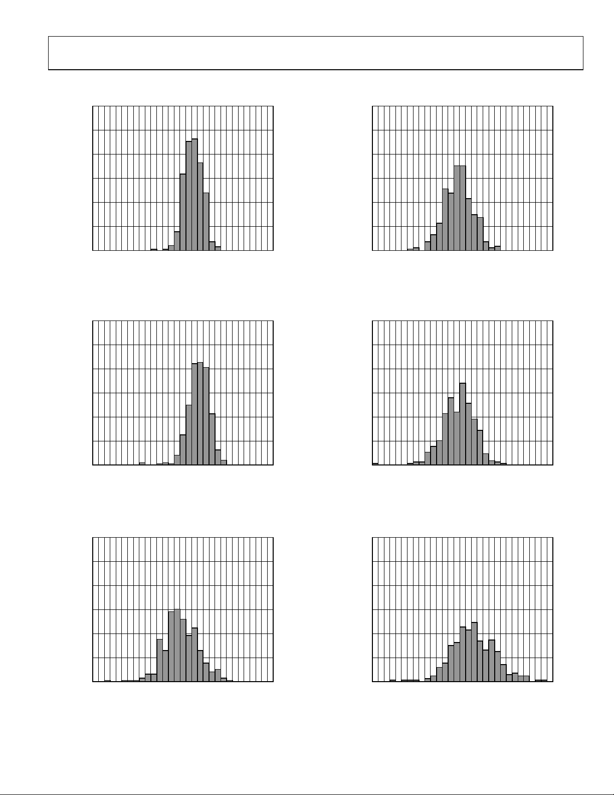
TYPICAL PERFORMANCE CHARACTERISTICS
30
30
25
20
15
10
PERCENT OF P OPULATION (%)
5
0
–150 –100 –50 0 50 100 150
ZERO g OFFSET (mg)
08167-004
25
20
TION (%)
15
10
PERCENT OF P OPUL
5
0
–150 –100 –50 0 50 100 150
ZERO g OFFSET (mg)
Figure 4. X-Axis Zero g Offset at 25°C, VS = 2.6 V Figure 7. X-Axis Zero g Offset at 25°C, VS = 1.8 V
30
25
20
15
10
30
25
20
TION (%)
15
10
08167-104
PERCENT OF P OPULATION (%)
5
0
–150 –100 –50 0 50 100 150
ZERO g OFFSET (mg)
08167-005
PERCENT OF P OPUL
5
0
–150 –100 –50 0 50 100 150
ZERO g OFFSET (mg)
Figure 5. Y-Axis Zero g Offset at 25°C, VS = 2.6 V Figure 8. Y-Axis Zero g Offset at 25°C, VS = 1.8 V
30
25
20
15
10
PERCENT OF P OPULATION (%)
5
0
–150 –100 –50 0 50 100 150
ZERO g OFFSET (mg)
Figure 6. Z-Axis Zero g Offset at 25°C, VS = 2.6 V
08167-006
30
25
20
TION (%)
15
10
PERCENT OF P OPUL
5
0
–150 –100 –50 0 50 100 150
ZERO g OFFSET (mg)
Figure 9. Z-Axis Zero g Offset at 25°C, V
= 1.8 V
S
08167-105
08167-106
Rev. 0 | Page 7 of 40

ADXL346
60
50
40
30
20
PERCENT OF POPULATION (%)
10
0
–3 –2 –1 0 1
ZERO g OFFSET TEMPERATURE COEFFICIENT (mg/°C)
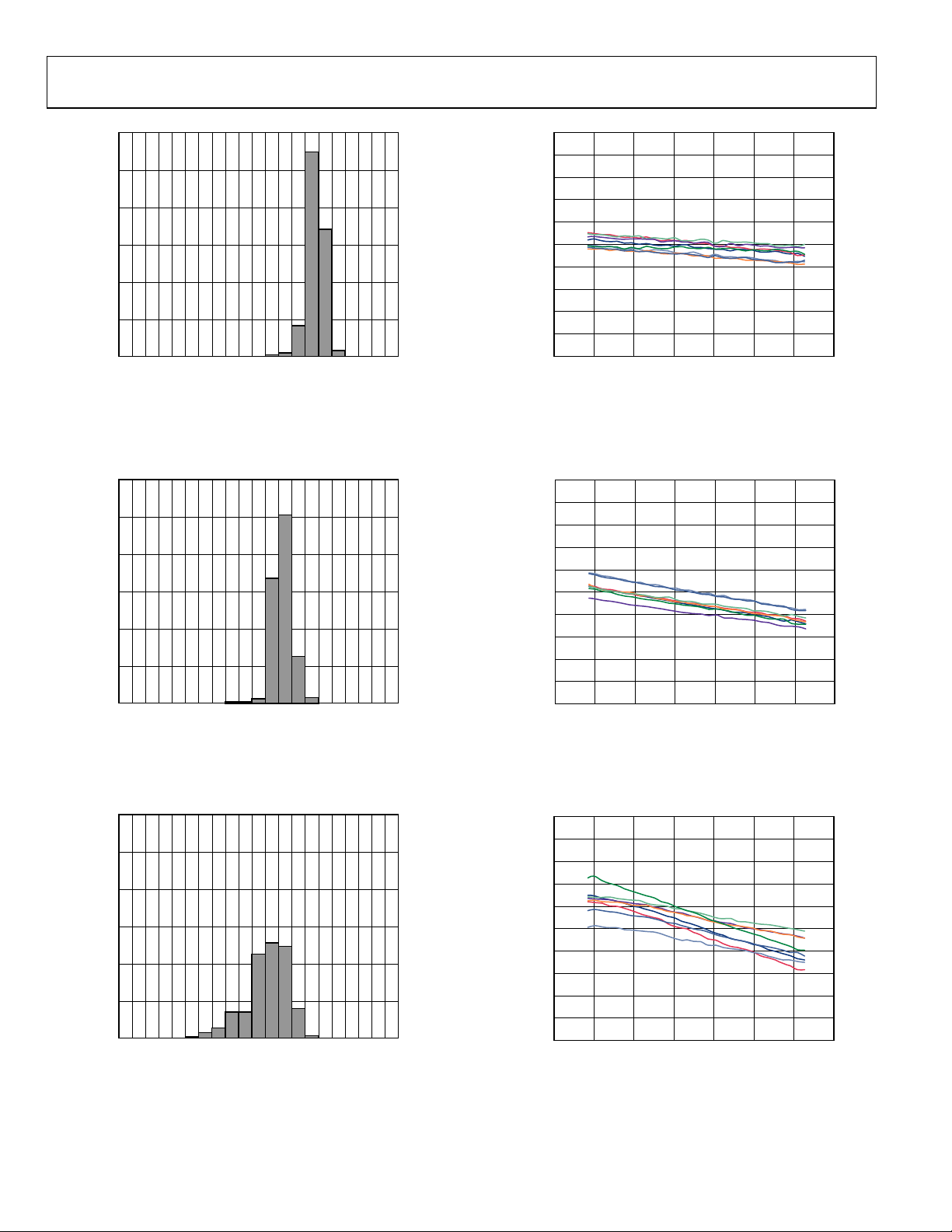
Figure 10. X-Axis Zero g Offset Temperature Coefficient, VS = 2.6 V
250
200
150
100
50
0
–50
ZERO g OFFSET (mg)
–100
–150
–200
08167-010
–250
–40 –20 0 20 40 60 80 100
TEMPERATURE (° C)
08167-013
Figure 13. X-Axis Zero g Offset vs. Temperature—
Eight Parts Soldered to PCB, V
= 2.6 V
S
60
50
40
30
20
PERCENT OF POPULATION (%)
10
0
–3 –2 –1 0 1
ZERO g OFFSET TEMPERATURE COEFFICIENT (mg/°C)
Figure 11. Y-Axis Zero g Offset Temperature Coefficient, VS = 2.6 V
60
50
40
30
20
PERCENT OF POPULATION (%)
10
0
–3 –2 –1 0 1
ZERO g OFFSET TEMPERATURE COEFFICIENT (mg/°C)
Figure 12. Z-Axis Zero g Offset Temperature Coefficient, VS = 2.6 V
250
200
150
100
50
0
–50
ZERO g OFFSET (mg)
–100
–150
–200
08167-011
–250
–40 –20 0 20 40 60 80 100
TEMPERATURE (°C)
08167-014
Figure 14. Y-Axis Zero g Offset vs. Temperature—
Eight Parts Soldered to PCB, V
250
200
150
100
50
0
–50
ZERO g OFFSET (mg)
–100
–150
–200
08167-012
–250
–40 –20 0 20 40 60 80 100
TEMPERATURE (° C)
= 2.6 V
S
08167-015
Figure 15. Z-Axis Zero g Offset vs. Temperature—
Eight Parts Soldered to PCB, V
= 2.6 V
S
Rev. 0 | Page 8 of 40

ADXL346
60
60
50
40
30
20
PERCENT OF POPUL AT I ON (%)
10
0
230 240 250 260 270 280
SENSITIVITY (LSB/g)
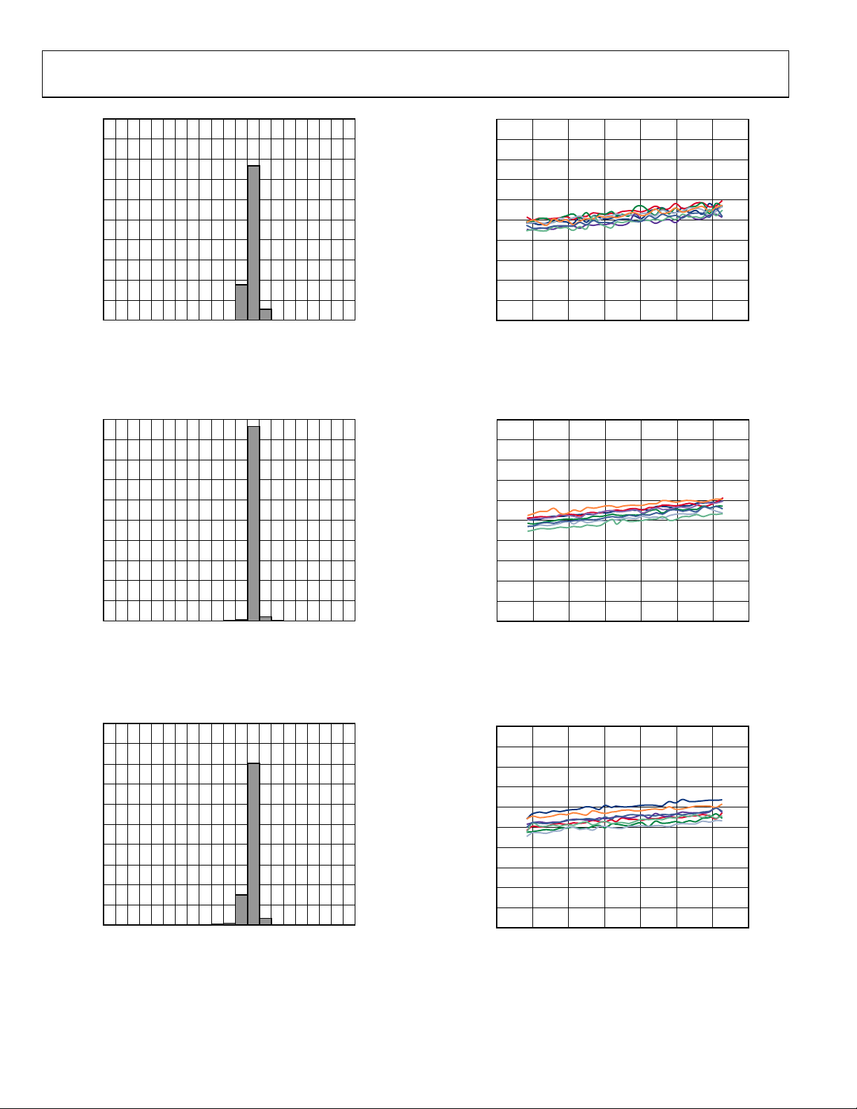
Figure 16. X-Axis Sensitivity at 25°C, VS = 2.6 V, Full Resolution
60
50
40
30
20
50
40
30
20
PERCENT OF POPUL AT I ON (%)
10
08167-016
0
230 240 250 260 270 280
SENSITIVITY (LSB/g)
08167-116
Figure 19. X-Axis Sensitivity at 25°C, VS = 1.8 V, Full Resolution
60
50
40
30
20
PERCENT OF POPUL AT I ON (%)
10
0
230 240 250 260 270 280
SENSITIVITY (LSB/g)
Figure 17. Y-Axis Sensitivity at 25°C, VS = 2.6 V, Full Resolution
60
50
40
30
20
PERCENT OF POPUL AT I ON (%)
10
0
230 240 250 260 270 280
SENSITIVITY (LSB/g)
Figure 18. Z-Axis Sensitivity at 25°C, VS = 2.6 V, Full Resolution
PERCENT OF POPUL AT I ON (%)
10
08167-017
0
230 240 250 260 270 280
SENSITIVITY (LSB/g)
08167-117
Figure 20. Y-Axis Sensitivity at 25°C, VS = 1.8 V, Full Resolution
60
50
40
30
20
PERCENT OF POPUL AT I ON (%)
10
08167-018
0
230 240 250 260 270 280
SENSITIVITY (LSB/g)
08167-118
Figure 21. Z-Axis Sensitivity at 25°C, VS = 1.8 V, Full Resolution
Rev. 0 | Page 9 of 40

ADXL346
100
90
80
70
60
50
40
30
20
PERCENT OF P OPULATION (%)
10
0
–0.10 –0.05 0 0.05 0.10
SENSITIV ITY TEMP E RATURE COEFFICIENT (%/°C)
Figure 22. X-Axis Sensitivity Temperature Coefficient, VS = 2.6 V
280
275
270
265
260
255
250
SENSITIVITY (LSB/g)
245
240
235
08167-022
230
–40 –20 0 20 40 60 80 100
TEMPERATURE (° C)
08167-025
Figure 25. X-Axis Sensitivity vs. Temperature—
Eight Parts Soldered to PCB, V
= 2.6 V, Full Resolution
S
100
90
80
70
60
50
40
30
20
PERCENT OF P OPULATION (%)
10
0
–0.10 –0.05 0 0.05 0.10
SENSITIV ITY TEMP E RATURE COEFFICIENT (%/°C)
Figure 23. Y-Axis Sensitivity Temperature Coefficient, VS = 2.6 V
100
90
80
70
60
50
40
30
20
PERCENT OF P OPULATION (%)
10
0
–0.10 –0.05 0 0.05 0.10
SENSITIV ITY TEMP E RATURE COEFFICIENT (%/°C)
Figure 24. Z-Axis Sensitivity Temperature Coefficient, VS = 2.6 V
280
275
270
265
260
255
250
SENSITIVITY (LSB/g)
245
240
235
08167-023
230
–40 –20 0 20 40 60 80 100
TEMPERATURE (°C)
08167-026
Figure 26. Y-Axis Sensitivity vs. Temperature—
Eight Parts Soldered to PCB, V
280
275
270
265
260
255
250
SENSITIVITY (LSB/g)
245
240
235
08167-024
230
–40 –20 0 20 40 60 80 100
TEMPERATURE (°C)
= 2.6 V, Full Resolution
S
08167-127
Figure 27. Z-Axis Sensitivity vs. Temperature—
Eight Parts Soldered to PCB, V
= 2.6 V, Full Resolution
S
Rev. 0 | Page 10 of 40

ADXL346
40
40
35
30
25
20
15
10
PERCENT OF POPULATION (%)
5
0
0.5 0.6 0.7 0.8 0.9 1.0
SELF-TEST SHIFT (
g)
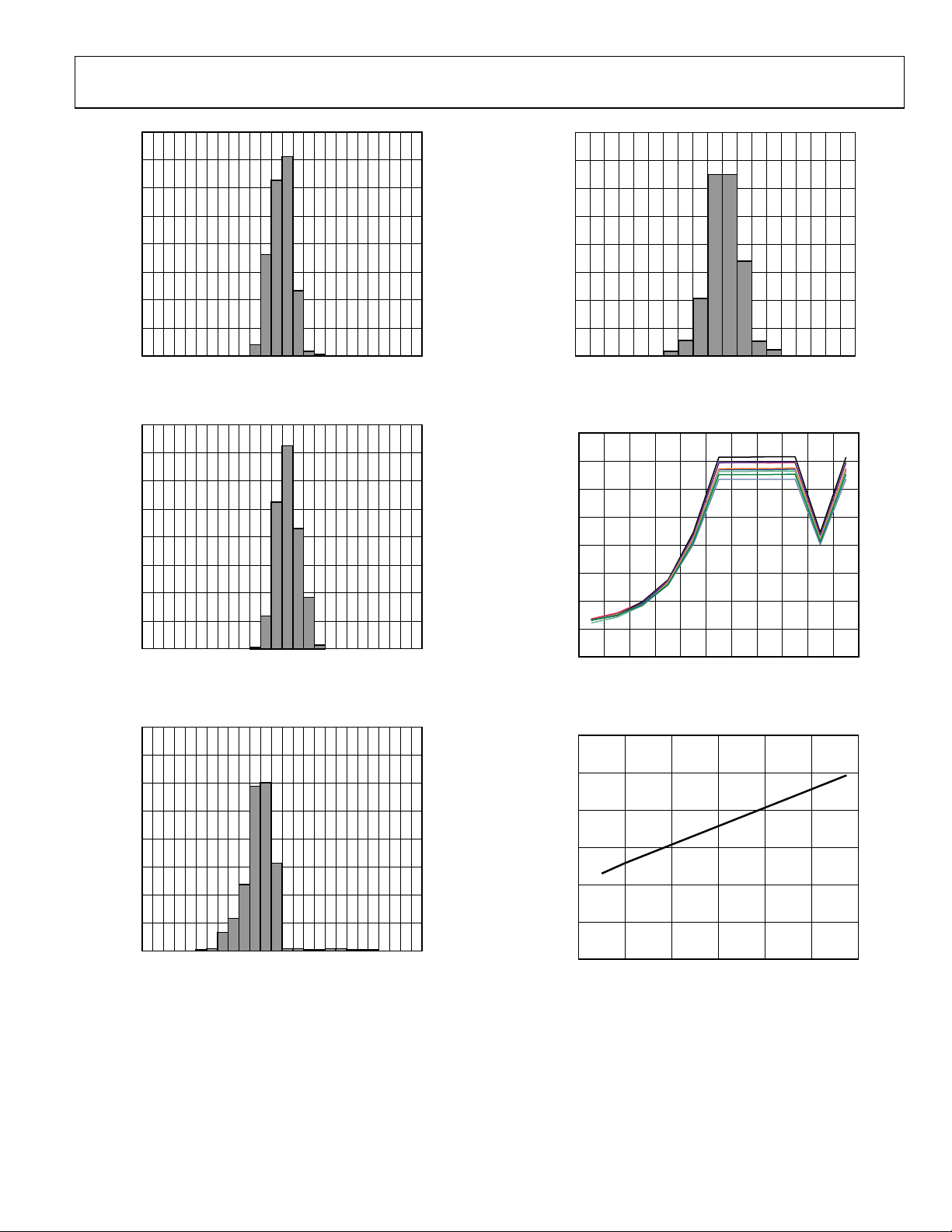
Figure 28. X-Axis Self-Test Response at 25°C, VS = 2.6 V
40
35
30
25
20
15
10
PERCENT OF POPULATION (%)
5
0
–1.0 –0.9 –0.8 –0.7 –0.6 –0.5
SELF-TEST SHIFT (
Figure 29. Y-Axis Self-Test Response at 25°C, V
40
35
30
g)
= 2.6 V
S
35
30
25
20
15
10
PERCENT OF P OPULATION (%)
5
08167-007
0
90 100 120 140 160 180110 130 150 170
OUTPUT CURRENT ( µ A)
Figure 31. Supply Current at 25°C, 100 Hz Output Data Rate, V
160
140
120
100
80
60
SUPPLY CURRENT (µA)
40
20
08167-008
0
3.13 6.25 12.50 25 50 100 200 400 1600800 3200
OUTPUT DATA RATE (Hz)
Figure 32. Supply Current vs. Output Data Rate at 25°C—10 Parts, V
150
140
= 2.6 V
S
= 2.6 V
S
08167-019
08167-020
25
20
15
10
PERCENT OF POPULATION (%)
5
0
1.0 1.1 1.2 1.3 1.51.4
SELF-TEST SHIFT (
Figure 30. Z-Axis Self-Test Response at 25°C, V
08167-009
g)
= 2.6 V
S
130
120
110
100
SUPPLY CURRENT CO NSUMPTION ( µA)
90
1.6 1.8 2.0 2.2 2.4 2.6 2.8
SUPPLY VOLTAGE, VS (V)
Figure 33. Supply Current vs. Supply Voltage at 25°C
08167-021
Rev. 0 | Page 11 of 40

ADXL346
THEORY OF OPERATION
The ADXL346 is a complete 3-axis acceleration measurement
system with a selectable measurement range of ±2 g, ±4 g, ±8 g,
or ±16 g. It measures both dynamic acceleration resulting from
motion or shock and static acceleration, such as gravity, which
allows the device to be used as a tilt sensor.
The sensor is a polysilicon surface-micromachined structure
built on top of a silicon wafer. Polysilicon springs suspend the
structure over the surface of the wafer and provide a resistance
against forces due to applied acceleration.
Deflection of the structure is measured using differential capacitors
that consist of independent fixed plates and plates attached to the
moving mass. Acceleration deflects the proof mass and unbalances
the differential capacitor, resulting in a sensor output with an
amplitude proportional to acceleration. Phase-sensitive demodulation is used to determine the magnitude and polarity
of the acceleration.
POWER SEQUENCING
Power can be applied to VS or V
damaging the ADXL346. All possible power-on modes are
summarized in Tab le 6. The interface voltage level is set with
the interface supply voltage, V
ensure that the ADXL346 does not create a conflict on the
communication bus. For single-supply operation, V
the same as the main supply, V
however, V
can differ from VS to accommodate the desired
DD I/O
interface voltage, as long as V
is applied, the device enters standby mode, where power
After V
S
consumption is minimized and the device waits for V
applied and for the command to enter measurement mode to be
received. (This command can be initiated by setting the measure
bit (Bit D3) in the POWER_CTL register (Address 0x2D).) In
addition, any register can be written to or read from to configure
the part while the device is in standby mode. It is recommended
to configure the device in standby mode and then to enable
measurement mode. Clearing the measure bit returns the
device to the standby mode.
in any sequence without
DD I/O
, which must be present to
DD I/O
DD I/O
. In a dual-supply application,
S
is greater than or equal to V
S
DD I/O
can be
DD I/O
to be
.
Table 6. Power Sequencing
Condition VS V
Power Off Off Off
Bus Disabled On Off
Bus Enabled Off On
Standby or
Measurement Mode
On On
Description
DD I/O
The device is completely off, but there is a potential for a communication
bus conflict.
The device is on in standby mode, but communication is unavailable and will
create a conflict on the communication bus. The duration of this state should
be minimized during power-up to prevent a conflict.
No functions are available, but the device will not create a conflict on the
communication bus.
At power-up, the device is in standby mode, awaiting a command to enter
measurement mode, and all sensor functions are off. After the device is
instructed to enter measurement mode, all sensor functions are available.
Rev. 0 | Page 12 of 40
 Loading...