Analog Devices ADV7173, ADV7172 Datasheet

Digital PAL/NTSC Video Encoder
with Six DACs (10 Bits), Color Control
a
FEATURES
1
ITU-R
BT601/656 YCrCb to PAL/NTSC Video Encoder
Six High Quality 10-Bit Video DACs
SSAF™ (Super Sub-Alias Filter)
Advanced Power Management Features
PC’98-Compliant (TV Detect with Polling and Auto
Shutdown to Save On Power Consumption)
Low Power DAC Mode
Individual DAC ON/OFF Control
Variable DAC Output Current (5 mA–36 mA)
Ultralow Sleep Mode Current
Hue, Brightness, Contrast and Saturation Controls
CGMS (Copy Generation Management System)
WSS (Wide Screen Signalling)
NTSC-M, PAL-M/N, PAL-B/D/G/H/I, PAL-60
YUV Betacam, MII and SMPTE Output Levels
Single 27 MHz Clock Required (ⴛ2 Oversampling)
80 dB Video SNR
32-Bit Direct Digital Synthesizer for Color Subcarrier
Multistandard Video Output Support:
Composite (CVBS)
Component S-Video (Y/C)
Component YUV
EuroSCART RGB
Component YUV + CHROMA + LUMA + CVBS
EuroSCART Output RGB + CHROMA + LUMA + CVBS
Programmable Clamping Output Signal
Advanced Programmable Power-On Reset Sequencing
Video Input Data Port Supports:
CCIR-656 4:2:2 8-Bit Parallel Input Format
SMPTE 170M NTSC-Compatible Composite Video
ITU-R BT.470 PAL-Compatible Composite Video
Luma Sharpness Control
Programmable Luma Filters (Low-Pass [PAL/NTSC],
Notch [PAL/NTSC], Extended [SSAF], CIF and QCIF)
Programmable Chroma Filters (Low-Pass [0.65 MHz,
1.0 MHz, 1.2 MHz and 2.0 MHz], CIF and QCIF)
Programmable VBI (Vertical Blanking Interval)
Programmable Subcarrier Frequency and Phase
Programmable LUMA Delay
CCIR and Square Pixel Operation
Integrated Subcarrier Locking to External Video Source
and Enhanced Power Management
ADV7172/ADV7173*
Color Signal Control/Burst Signal Control
Interlaced/Noninterlaced Operation
Complete On-Chip Video Timing Generator
Programmable Multimode Master/Slave Operation
Macrovision AntiTaping Rev 7.01 (ADV7172 Only)
Closed Captioning Support
Teletext Insertion Port (PAL-WST)
On-Board Color Bar Generation
On-Board Voltage Reference
2-Wire Serial MPU Interface (I
Single Supply +5 V or +3.3 V Operation
Small 48-Lead LQFP Package
APPLICATIONS
High Performance DVD Playback Systems, Portable
Video Equipment including Digital Still Cameras and
Laptop PCs, Video Games, PC Video/Multimedia and
Digital Satellite/Cable Systems (Set-Top Boxes/IRD)
GENERAL DESCRIPTION
The ADV7172/ADV7173 is an integrated Digital Video Encoder that converts digital CCIR-601 4:2:2 8-bit component
video data into a standard analog baseband television signal
compatible with world wide standards.
There are six DACs available on the ADV7172/ADV7173. In
addition to the Composite output signal there is the facility to
output S-VHS Y/C Video, RGB Video and YUV Video.
The on-board SSAF (Super Sub-Alias Filter), with extended
luminance frequency response and sharp stopband attenuation,
enables studio quality video playback on modern TVs, giving
optimal horizontal line resolution. An additional sharpness
control feature allows extra luminance boost on the frequency
response.
An advanced power management circuit enables optimal control
of power consumption in both normal operating modes and
power down or sleep modes. A PC’98-Compliant autodetect
feature has been added to allow the user to determine whether
or not the DACs are correctly terminated. If not, the ADV7172/
ADV7173 flags that they are not connected through the Status
bit and provides the option of automatically powering them
down, thereby reducing power consumption.
2C®
Compatible and Fast I2C)
2
NOTES
*This device is protected by U.S. Patent Numbers 4,631,603, 4,577,216, 4,819,098 and other intellectual property rights.
1
ITU-R and CCIR are used interchangeably in this document (ITU-R has replaced CCIR recommendations).
2
The Macrovision anticopy process is licensed for noncommercial home use only, which is its sole intended use in the device. Please contact sales office for latest
Macrovision version available.
SSAF is a trademark of Analog Devices, Inc.
I2C is a registered trademark of Philips Corporation.
REV. A
Information furnished by Analog Devices is believed to be accurate and
reliable. However, no responsibility is assumed by Analog Devices for its
use, nor for any infringements of patents or other rights of third parties
which may result from its use. No license is granted by implication or
otherwise under any patent or patent rights of Analog Devices.
One Technology Way, P.O. Box 9106, Norwood, MA 02062-9106, U.S.A.
Tel: 781/329-4700 World Wide Web Site: http://www.analog.com
Fax: 781/326-8703 © Analog Devices, Inc., 1999
ADV7172/ADV7173
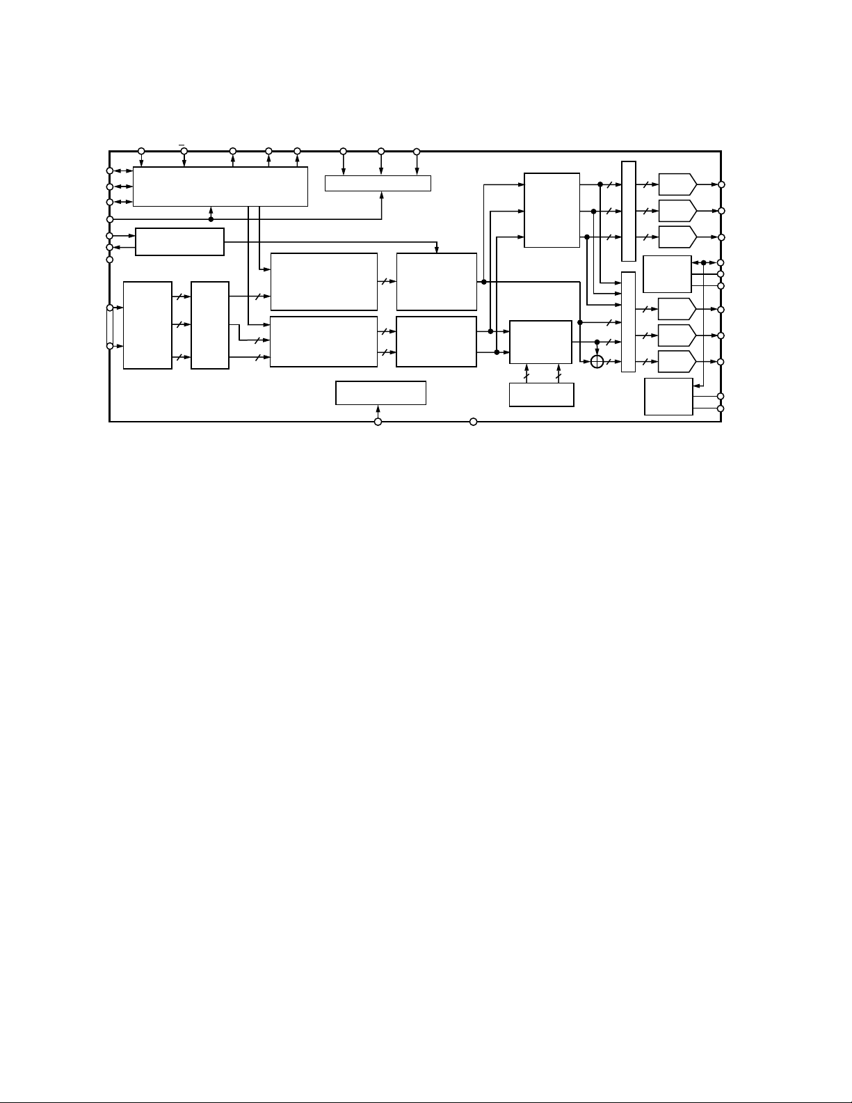
FUNCTIONAL BLOCK DIAGRAM
HSYNC
FIELD/
VSYNC
BLANK
RESET
TTX
TTXREQ
V
COLOR
DATA
CLOCK CSO_HSO VSO
PAL NTSC
VIDEO TIMING
GENERATOR
TELETEXT
INSERTION BLOCK
AA
8
P0
4:2:2 TO
INTER-
POLATOR
P7
4:4:4
8
MATRIX
8
ADV7172/ADV7173
YCrCb
TO
YUV
CLAMP
CONTRAST CONTROL
Y
8
U
V
SATURATION CONTROL
8
8
SCLOCK SDATA
I2C MPU PORT
BRIGHTNESS AND
+
ADD SYNC
+
INTERPOLATOR
+
ADD BURST
+
INTERPOLATOR
CONTROL CIRCUIT
SCRESET/RTC
REAL-TIME
ALSB
PROGRAMMABLE
10
SHARPNESS
10
PROGRAMMABLE
10
The ADV7172/ADV7173 also supports both PAL and NTSC
square pixel operation. The parts also incorporate WSS and
CGMS-A data control generation.
The ADV7172/ADV7173 is designed with four color controls
(hue, contrast, brightness and saturation). All YUV formats
(SMPTE, MII and Betacam) are supported in both PAL and
NTSC.
The output video frames are synchronized with the incoming
data Timing Reference Codes. Optionally the encoder accepts
(and can generate) HSYNC , VSYNC and FIELD timing
signals. These timing signals can be adjusted to change pulsewidth and position while the part is in the master mode. The
Encoder requires a single two times pixel rate (27 MHz) clock
for standard operation. Alternatively the Encoder requires a
24.54 MHz clock for NTSC or 29.5 MHz clock for PAL square
pixel mode operation. All internal timing is generated on-chip.
HSO/CSO and VSO TTL outputs, synchronous to the analog
output video, are also available. A programmable CLAMP
output signal is also available to enable clamping in either the
front or back porch of the video signal.
A separate teletext port enables the user to directly input teletext data during the vertical blanking interval.
The ADV7172/ADV7173 modes are set up over a two wire
serial bidirectional port (I
2
C-Compatible) with two slave addresses. Functionally the ADV7173 and ADV7172 are the same
with the exception that the ADV7172 can output the Macrovision anticopy algorithm.
The ADV7172/ADV7173 is packaged in a 48-lead LQFP package (1.4 mm thickness).
DATA PATH DESCRIPTION
For PAL B, D, G, H, I, M, N and NTSC M, N modes, YCrCb
4:2:2 Data is input via the CCIR-656-Compatible Pixel Port at
a 27 MHz Data Rate. The Pixel Data is demultiplexed to form
three data paths. Y typically has a range of 16 to 235, Cr and
M
10
10
U
L
T
I
P
L
E
X
E
R
M
U
L
T
I
P
L
E
X
E
R
10-BIT
10
10-BIT
10
10-BIT
DAC
CONTROL
BLOCK
10
10-BIT
10
10-BIT
10
10-BIT
DAC
CONTROL
BLOCK
DAC
DAC
DAC
DAC
DAC
DAC
DAC A
DAC B
DAC C
V
REF
R
SET2
COMP2
DAC E
DAC F
DAC D
R
SET1
COMP1
LUMA
FILTER
+
FILTER
CHROMA
FILTER
GND
YUV TO
RBG
MATRIX
+
YUV
LEVEL
CONTROL
BLOCK
MODULATOR
+
HUE
CONTROL
10 10
SIN/COS
DDS BLOCK
10
10
10
10
10
Cb typically have a range of 128 ± 112; however, it is possible
to input data from 1 to 254 on both Y, Cb and Cr. The ADV7172/
ADV7173 supports PAL (B, D, G, H, I, N, M) and NTSC
(with and without pedestal) standards. The Y data is then manipulated by being scaled for contrast control and a setup level
is added for brightness control. The Cr, Cb data is also scaled
and saturation control is added. The appropriate Sync, Blank
and Burst levels are then added to the YCrCb data. Macrovision AntiTaping (ADV7172 only), Closed-Captioning and
Teletext levels are also added to Y, and the resultant data is
interpolated to a rate of 27 MHz. The interpolated data is filtered and scaled by three digital FIR Filters.
The U and V Signals are modulated by the appropriate subcarrier sine/cosine phases and a phase offset may be added onto
the color subcarrier during active video to allow hue adjustment.
The resulting U and V signals are then added together to make
up the chrominance signal. The luma (Y) signal can be delayed
1–3 luma cycles (each cycle is 74 ns) with respect to the chroma
signal. The luma and chroma signals are then added together to
make up the composite video signal. All edges are slew rate
limited.
The YCrCb data is also used to generate RGB data with appropriate Sync and Blank levels. The YUV levels are also scaled to
output the suitable SMPTE or Betacam levels.
There are six DACs on the ADV7172/ADV7173. Three of these
DACs are capable of providing 34.66 mA of current. The other
three DACs provide 8.66 mA each.
The six l0-bit DACs can be used to output:
1. Composite Video + RGB Video + LUMA + CHROMA.
2. Composite Video + YUV Video + LUMA + CHROMA.
Alternatively, each DAC can be individually powered off if not
required. A complete description of DAC output configurations
is given in Appendix 8.
Video output levels are illustrated in Appendix 6.
(continued on page 11)
–2– REV. A

SPECIFICATIONS
(VAA = +5 V ⴞ 5%1, V
5 V SPECIFICATIONS
unless otherwise noted)
Parameter Test Conditions
= 1.235 V, R
REF
= 600 ⍀ unless otherwise noted. All specifications T
SET1,2
1
Min Typ Max Units
ADV7172/ADV7173
STATIC PERFORMANCE
Resolution (Each DAC) 10 Bits
Accuracy (Each DAC)
Integral Nonlinearity
Differential Nonlinearity
3
3
Guaranteed Monotonic ±1.0 LSB
±1.0 LSB
DIGITAL INPUTS
Input High Voltage, V
Input Low Voltage, V
Input Current, I
Input Capacitance, C
INL
IN
IN
INH
V
= 0.4 V or 2.4 V ±1 µA
IN
2V
0.8 V
10 pF
DIGITAL OUTPUTS
Output High Voltage, V
Output Low Voltage, V
OL
OH
I
I
= 400 µA 2.4 V
SOURCE
= 3.2 mA 0.4 V
SINK
Three-State Leakage Current 10 µA
Three-State Output Capacitance 10 pF
ANALOG OUTPUTS
Output Current (DACs A, B, C)
Output Current (DACs A, B, C)
Output Current (DACs D, E, F)
Output Current (DACs D, E, F)
DAC-to-DAC Matching (DACs A, B, C)
DAC-to-DAC Matching (DACs D, E, F)
Output Compliance, V
Output Impedance, R
Output Capacitance, C
OC
OUT
OUT
4
5
6
5
R
= 150 Ω, RL = 37.5 Ω 33 34.7 37 mA
SET1
R
= 1041 Ω, RL = 262.5 Ω 5mA
SET1
R
= 600 Ω, RL = 150 Ω 8.25 8.66 9.25 mA
SET2
R
= 1041 Ω, RL = 262.5 Ω 5mA
SET2
7
7
1 4.0 %
1 4.0 %
0 +1.4 V
30 kΩ
I
= 0 mA 30 pF
OUT
VOLTAGE REFERENCE
Reference Range, V
REF
I
VREFOUT
= 20 µA 1.112 1.235 1.359 V
POWER REQUIREMENTS
V
AA
Normal Power Mode
I
DAC
I
DAC
I
CCT
Low Power Mode
I
DAC
I
DAC
I
CCT
Sleep Mode
I
DAC
I
CCT
(max)
(min)
10
(max)
(min)
10
12
13
8, 9
8, 9
11
11
R
= 600 Ω 59 65 mA
SET1,2
R
= 1041 Ω 30 mA
SET1,2
R
= 150 Ω 64 mA
SET1
4.75 5.0 5.25 V
78 90 mA
15 mA
78 90 mA
0.1 µA
0.1 µA
Power Supply Rejection Ratio COMP = 0.1 µF 0.01 0.5 %/%
NOTES
1
The max/min specifications are guaranteed over this range. The max/min values are typical over 4.75 V to 5.25 V.
2
Temperature range T
3
Characterized by design.
4
Full
drive into 75 Ω doubly terminated load.
5
Minimum drive current (used with buffered/scaled output load).
6
Full drive into 150 Ω load.
7
Specification guaranteed by characterization.
8
I
is the total current (“min” corresponds to 5 mA output per DAC, “max” corresponds to 8.66 mA output per DAC ) to drive DACs A, B, C, D, E, F. Turning off
DAC
individual DACs reduces I
9
All six DACs on (DAC A, B, C, D, E, F).
10
I
(Circuit Current) is the continuous current required to drive the device.
CCT
11
Only large DACs (DACs A, B, C) on per low power mode.
12
Total DAC current in Sleep Mode.
13
Total continuous current during Sleep Mode.
Specifications subject to change without notice.
to T
MIN
: 0°C to +70°C.
MAX
correspondingly, also DACs A, B, C can be configured to output a max current of 37 mA but DAC D, E, F must be turned off.
DAC
MIN
to T
MAX
2
–3–REV. A

ADV7172/ADV7173–SPECIFICATIONS
(VAA = +3.0 V–3.6 V1, V
3.3 V SPECIFICATIONS
unless otherwise noted)
Parameter Test Conditions
STATIC PERFORMANCE
3
Resolution (Each DAC) 10 Bits
Accuracy (Each DAC)
Integral Nonlinearity 1.0 LSB
Differential Nonlinearity Guaranteed Monotonic 1.0 LSB
DIGITAL INPUTS
Input High Voltage, V
Input Low Voltage, V
Input Current, I
Input Capacitance, C
DIGITAL OUTPUTS
Output High Voltage, V
Output Low Voltage, V
3
INH
INL
IN
IN
3
OH
OL
V
I
I
Three-State Leakage Current 10 µA
Three-State Output Capacitance 10 pF
8
8, 9
3
OC
OUT
OUT
3, 7
4
5
6
5
R
R
R
R
3
3
I
R
R
ANALOG OUTPUTS
Output Current (DACs A, B, C)
Output Current (DACs A, B, C)
Output Current (DACs D, E, F)
Output Current (DACs D, E, F)
DAC-to-DAC Matching (DACs A, B, C)
DAC-to-DAC Matching (DACs D, E, F)
Output Compliance, V
Output Impedance, R
Output Capacitance, C
POWER REQUIREMENTS
V
AA
Normal Power Mode
(max)
I
DAC
(min)
I
DAC
10
I
CCT
Sleep Mode
11
I
DAC
12
I
CCT
Power Supply Rejection Ratio COMP = 0.1 µF 0.01 %/%
NOTES
1
The max/min specifications are guaranteed over this range. The max/min values are typical over 3.0 V to 3.6 V.
2
Temperature range T
3
Guaranteed by characterization.
4
Full
drive into 75␣ Ω doubly terminated load.
5
Minimum drive current (used with buffered/scaled output load).
6
Full Drive into 150 Ω load.
7
Power measurements are taken with Clock Frequency = 27 MHz. Max T
8
I
is the total current (“min” corresponds to 5 mA output per DAC, “max” corresponds to 8.66 mA output per DAC ) to drive DACs A, B, C, D, E, F. Turning off
DAC
individual DACs reduces I
9
DACs A, B, C can output 35 mA typically at 3.3 V (R
R
= 75 Ω).
L
10
I
(Circuit Current) is the continuous current required to drive the device.
CCT
11
Total DAC current in Sleep Mode.
12
Total continuous current during Sleep Mode.
Specifications subject to change without notice.
to T
MIN
: 0°C to +70°C.
MAX
correspondingly, also DACs A, B, C can be configured to output a max current of 37 mA.
DAC
= 150 Ω and RL = 37.5 Ω), optimum performance obtained at 18 mA DAC Current (R
SET
= 1.235 V, R
REF
= 600 ⍀ unless otherwise noted. All specifications T
SET1,2
1
Min Typ Max Units
2V
0.8 V
= 0.4 V or 2.4 V ±1 µA
IN
10 pF
= 400 µA 2.4 V
SOURCE
= 3.2 mA 0.4 V
SINK
= 150 Ω, RL = 37.5 Ω 34.7 mA
SET1
= 1041 Ω, RL = 262.5 Ω 5mA
SET1
= 600 Ω, RL = 150 Ω 8.66 mA
SET2
= 1041 Ω, RL = 262.5 Ω 5mA
SET2
1 4.0 %
1 4.0 %
+1.4 V
30 kΩ
= 0 mA 30 pF
OUT
3.0 3.3 3.6 V
= 600 Ω 58 65 mA
SET1,2
= 1041 Ω 30 mA
SET1,2
40 mA
0.1 µA
0.1 µA
= 110°C.
J
= 300 Ω and
SET
MIN
to T
MAX
2
–4– REV. A

ADV7172/ADV7173
(VAA = +5 V ⴞ 5%1, V
5 V DYNAMIC SPECIFICATIONS
Parameter Conditions
3, 4
3, 4
3, 4
3, 4
3, 4
MIN
3, 4
3, 4
3, 4
3, 4
to T
3, 4
3, 4
3, 4
3, 4
3, 4
: 0°C to +70°C.
MAX
Differential Gain
Differential Phase
Differential Gain
Differential Phase
3, 4
(Pedestal) RMS 75 dB rms
SNR
3, 4
(Pedestal) Peak Periodic 66 dB p-p
SNR
3, 4
(Ramp) RMS 60 dB rms
SNR
3, 4
(Ramp) Peak Periodic 58 dB p-p
SNR
Hue Accuracy
Color Saturation Accuracy
Chroma Nonlinear Gain
Chroma Nonlinear Phase
Chroma/Luma Intermod
Chroma/Luma Gain Inequality
Chroma/Luma Delay Inequality
Luminance Nonlinearity
Chroma AM Noise
Chroma PM Noise
NOTES
1
The max/min specifications are guaranteed over this range. The max/min values are typical over 4.75 V to 5.25 V range.
2
Temperature range T
3
These specifications are for the low-pass filter only and guaranteed by design.
4
Guaranteed by characterization.
Specifications subject to change without notice.
specifications T
1
Normal Power Mode 0.3 0.7 %
Normal Power Mode 0.4 0.7 Degrees
Lower Power Mode 0.5 1.0 %
Lower Power Mode 2.0 3.0 Degrees
Referenced to 40 IRE 1.2 ±%
MIN
to T
= 1.235 V, R
REF
2
unless otherwise noted.)
MAX
SET1,2
Min Typ Max Units
79 82 dB
79 80 dB
= 600 ⍀ unless otherwise noted. All
0.7 Degrees
0.9 %
0.3 0.5 ±Degrees
0.2 0.4 ±%
1.0 ±%
0.5 ns
1.0 1.7 ±%
(VAA = +3.0 V – 3.6 V1, V
3.3 V DYNAMIC SPECIFICATIONS
Parameter Conditions
Differential Gain
Differential Phase
Differential Gain
Differential Phase
3
(Pedestal) RMS 75 dB rms
SNR
3
(Pedestal) Peak Periodic 70 dB p-p
SNR
3
(Ramp) RMS 60 dB rms
SNR
3
(Ramp) Peak Periodic 58 dB p-p
SNR
Hue Accuracy
Color Saturation Accuracy
Luminance Nonlinearity
Chroma AM Noise
Chroma PM Noise
Chroma Nonlinear Gain
Chroma Nonlinear Phase
Chroma/Luma Intermod
NOTES
1
The max/min specification are guaranteed over this range. The max with values are typical over a 3.0 V to 3.6 V range.
2
Temperature range T
3
Guaranteed by characterization.
4
These specifications are for the low-pass filter only and guaranteed by design.
Specifications subject to change without notice.
3
3
3
3
3
3
3
3
3
3, 4
3, 4
3, 4
to T
MIN
: 0°C to +70°C.
MAX
specifications T
1
MIN
Normal Power Mode 0.6 %
Normal Power Mode 0.5 Degrees
Lower Power Mode 1.0 %
Lower Power Mode 0.5 Degrees
Referenced to 40 IRE 1.2 ±%
to T
= 1.235 V, R
REF
2
unless otherwise noted.)
MAX
SET1,2
Min Typ Max Units
= 600 ⍀ unless otherwise noted. All
1.0 Degrees
1.0 %
1.1 ±%
83 dB
79 dB
0.3 ±Degrees
0.2 ±%
–5–REV. A

ADV7172/ADV7173
5 V TIMING SPECIFICATIONS
(VAA = +5 V ⴞ 5%1, V
T
MIN
2
to T
unless otherwise noted.)
MAX
= 1.235 V, R
REF
= 600 ⍀ unless otherwise noted. All specifications
SET1
Parameter Conditions Min Typ Max Units
MPU PORT
3, 4
SCLOCK Frequency 0 400 kHz
SCLOCK High Pulsewidth, t
SCLOCK Low Pulsewidth, t
Hold Time (Start Condition), t
Setup Time (Start Condition), t
Data Setup Time, t
5
SDATA, SCLOCK Rise Time, t
SDATA, SCLOCK Fall Time, t
Setup Time (Stop Condition), t
ANALOG OUTPUTS
3, 5
1
2
After this period the 1st clock is generated 0.6 µs
3
relevant for repeated Start Condition. 0.6 µs
4
6
7
8
0.6 µs
1.3 µs
100 ns
300 ns
300 ns
0.6 µs
Analog Output Delay 7ns
DAC Analog Output Skew 0 ns
CLOCK CONTROL AND
PIXEL PORT
f
CLOCK
Clock High Time, t
Clock Low Time, t
Data Setup Time, t
Data Hold Time, t
Control Setup Time, t
Control Hold Time, t
Digital Output Access Time, t
Digital Output Hold Time, t
Pipeline Delay, t
TELETEXT PORT
Digital Output Access Time, t
Data Setup Time, t
Data Hold Time, t
RESET CONTROL
5, 6
27 MHz
9
10
11
12
11
12
13
14
15
3, 7
16
17
18
3
8ns
8ns
4.0 ns
5.0 ns
4ns
3ns
15 24 ns
10 ns
37 Clock Cycles
20 ns
2ns
6ns
RESET Low Time 3ns
NOTES
1
The max/min specifications are guaranteed over this range. The max/min values are typical over 4.75 V to 5.25 V range.
2
Temperature range T
3
TTL input values are 0 to 3 volts, with input rise/fall times ≤ 3 ns, measured between the 10% and 90% points. Timing reference points at 50% for inputs and
outputs. Analog output load ≤ 10 pF.
4
Guaranteed by characterization.
5
Output delay measured from the 50% point of the rising edge of CLOCK to the 50% point of full-scale transition.
6
Pixel Port consists of the following:
Pixel Inputs: P7–P0
Pixel Controls: HSYNC, FIELD/VSYNC, BLANK, VSO, CSO_HSO, CLAMP
Clock Input: CLOCK
7
Teletext Port consists of the following:
Teletext Output: TTXREQ
Teletext Input: TTX
Specifications subject to change without notice.
MIN
to T
: 0°C to +70°C.
MAX
–6– REV. A

ADV7172/ADV7173
to T
MAX
2
unless
3.3 V TIMING SPECIFICATIONS
(VAA = +3.0 V–3.6 V1, V
otherwise noted.)
= 1.235 V, R
REF
= 600 ⍀. All specifications T
SET1,2
MIN
Parameter Conditions Min Typ Max Units
MPU PORT
3, 4
SCLOCK Frequency 0 400 kHz
SCLOCK High Pulsewidth, t
SCLOCK Low Pulsewidth, t
Hold Time (Start Condition), t
Setup Time (Start Condition), t
Data Setup Time, t
5
SDATA, SCLOCK Rise Time, t
SDATA, SCLOCK Fall Time, t
Setup Time (Stop Condition), t
ANALOG OUTPUTS
3, 5
1
2
3
After this period the 1st clock is generated 0.6 µs
relevant for repeated Start Condition. 0.6 µs
4
6
7
8
0.6 µs
1.3 µs
100 ns
300 ns
300 ns
0.6 µs
Analog Output Delay 7ns
DAC Analog Output Skew 0 ns
CLOCK CONTROL AND
PIXEL PORT
f
CLOCK
Clock High Time, t
Clock Low Time, t
Data Setup Time, t
Data Hold Time, t
Control Setup Time, t
Control Hold Time, t
Digital Output Access Time, t
Digital Output Hold Time, t
Pipeline Delay, t
TELETEXT PORT
Digital Output Access Time, t
Data Setup Time, t
Data Hold Time, t
RESET CONTROL
4, 5, 6
15
9
10
11
12
3, 4, 7
17
18
3, 4
27 MHz
8ns
8ns
4.0 ns
5ns
11
12
13
14
5ns
3ns
20 ns
12 ns
37 Clock Cycles
16
23 ns
2ns
6ns
RESET Low Time 3ns
NOTES
1
The max/min specifications are guaranteed over this range. The max/min values are typical over 3.0 V to 3.6 V range.
2
Temperature range T
3
TTL input values are 0 to 3 volts, with input rise/fall times ≤ 3 ns, measured between the 10% and 90% points. Timing reference points at 50% for inputs and
outputs. Analog output load ≤ 10 pF.
4
Guaranteed by characterization.
5
Output delay measured from the 50% point of the rising edge of CLOCK to the 50% point of full-scale transition.
6
Pixel Port consists of the following:
Pixel Inputs: P7–P0
Pixel Controls: HSYNC, FIELD/VSYNC, BLANK, VSO, CSO_HSO, CLAMP
Clock Input: CLOCK
7
Teletext Port consists of the following:
Teletext Output: TTXREQ
Teletext Input: TTX
Specifications subject to change without notice.
MIN
to T
: 0°C to +70°C.
MAX
–7–REV. A
ADV7172/ADV7173
SDATA
SCLOCK
CLOCK
t
t
3
t
6
t
2
5
t
1
t
7
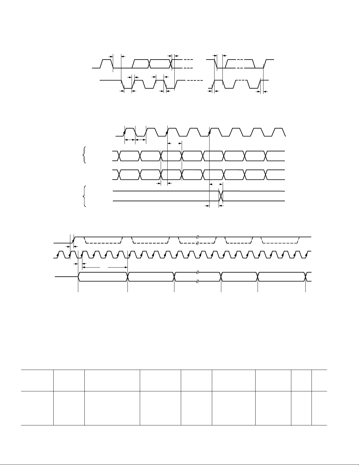
Figure 1. MPU Port Timing Diagram
t
3
t
4 t
8
TXTREQ
CLOCK
TXT
CONTROL
CONTROL
t
16
t
12
t
11
t
13
t
14
I/PS
O/PS
HSYNC,
FIELD/VSYNC,
BLANK
PIXEL INPUT
DATA
HSYNC,
FIELD/VSYNC,
BLANK,
CSO_HSO,
VSO, CLAMP
t
t
9
10
Cb Y Cr Y Cb Y
Figure 2. Pixel and Control Data Timing Diagram
t
17
t
18
4 CLOCK
CYCLES
4 CLOCK
CYCLES
4 CLOCK
CYCLES
3 CLOCK
CYCLES
4 CLOCK
CYCLES
Figure 3. Teletext Timing Diagram
DAC Average Current Consumption
DAC D, E, F: The average current consumed by each DAC is the DAC output current as determined by R
SET2/VREF
DAC A, B, C: In normal power mode the average current consumed by each DAC is the DAC output current as determined by R
(see Appendix 8).
SET1
(see Appendix 8).
In Low Power Mode the average current consumed by each DAC is approximately half the DAC output current as determined by R
SET1.
Table I. Allowable Operating Configurations
Average Average
DACs Output DAC Current DACs Output DAC Current Power
A, B, C Current Consumption D, E, F Current Consumption Mode 5 V? 3 V?
3 DACs ON 37 mA See Above 3 DACs ON 8.66 mA See Above Normal No Yes
3 DACs ON 37 mA 18.5 mA (See Above) 3 DACs ON 8.66 mA See Above Low Power No Yes
3 DACs ON 37 mA 18.5 mA (See Above) 3 DACs OFF See Above Low Power Yes Yes
3 DACs ON 8.66 mA See Above 3 DACs ON 8.66 mA See Above Normal Yes Yes
3 DACs ON 4.33 mA See Above 3 DACs ON 4.33 mA See Above Normal Yes Yes
–8– REV. A
ADV7172/ADV7173
WARNING!
ESD SENSITIVE DEVICE
ABSOLUTE MAXIMUM RATINGS
1
VAA to GND . . . . . . . . . . . . . . . . . . . . . . . . . . . . . . . . . . . 7 V
Voltage on Any Digital Input Pin . GND – 0.5 V to V
Storage Temperature (T
Junction Temperature (T
Lead Temperature (Soldering, 10 sec) . . . . . . . . . . . . +260°C
Analog Outputs to GND
NOTES
1
Stresses above those listed under Absolute Maximum Ratings may cause permanent
damage to the device. This is a stress rating only; functional operation of the device
at these or any other conditions above those listed in the operational sections of this
specification is not implied. Exposure to absolute maximum rating conditions for
extended periods may affect device reliability.
2
Analog output short circuit to any power supply or common can be of an indefinite
duration.
) . . . . . . . . . . . . . . –65°C to +150°C
S
) . . . . . . . . . . . . . . . . . . . . . +150°C
J
2
␣ . . . . . . . . . . . GND – 0.5 V to V
+ 0.5 V
AA
AA
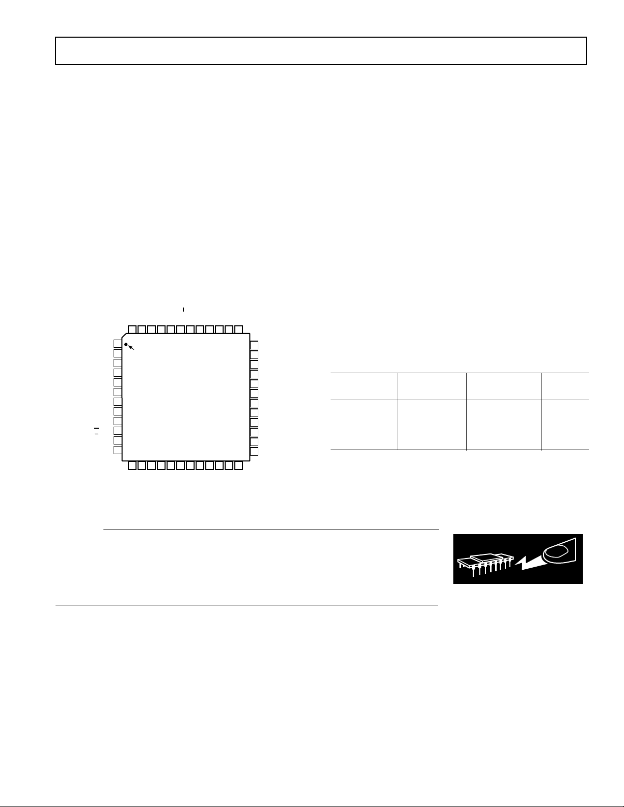
PIN CONFIGURATION
NTSC
SET1
R
SCRESET/RTC
TTXREQ
SET2
R
SDATA
COMP2
REF
V
36
35
34
33
32
31
30
29
28
27
26
25
DAC F
COMP1
DAC A
V
AA
DAC B
V
AA
GND
V
AA
DAC C
DAC D
V
AA
GND
DAC E
CSO
V
HSO
V
GND
AA
CLOCK
GND
RESET
V
48 47 46 45 44 39 38 3743 42 41 40
1
AA
2
P0
3
P1
4
P2
5
P3
6
P4
7
P5
8
P6
9
P7
10
11
AA
12
13 14 15 16 17 18 19 20 21 22 23 24
VSO
PIN 1
IDENTIFIER
ADV7172/ADV7173
TOP VIEW
(Not to Scale)
GND
HSYNC
FIELD/VSYNC
ALSB
BLANK
PAL
GND
CLAMP
TTX
AA
V
SCLOCK
PACKAGE THERMAL PERFORMANCE
The 48-lead LQFP package is used for this device. The junction-
to-ambient (θ
) thermal resistance in still air on a four layer
JA
PCB is +54.6°C/W. The junction-to-case thermal resistance
) is +16.7°C.
(θ
JC
To reduce power consumption when using this part the user is
advised to run the part on a 3.3 V supply, turn off any unused
DACs. However, if 5 V operation is required the user can enable
Low Power mode by setting MR16 to a Logic 1. Another alternative way to further reduce power is to use external buffers that
dramatically reduce the DAC currents, the current can be lowered to as low as 5 mA (see Appendix 8 for more details) from a
nominal value of 36 mA.
The user must at all times stay below the maximum junction
temperature of +110°C. The following equation shows how to
calculate this junction temperature:
J
unction Temperature = [VAA (I
DAC
+ I
CCT
) × θJA ] +70°C
where
= 10 mA + (sum of the average currents consumed by each
I
DAC
powered-on DAC).
ORDERING GUIDE
Temperature Package Package
Model Range Description Option
ADV7172KST 0°C to +70°C Plastic Thin ST-48
Quad Flatpack
ADV7173KST 0°C to +70°C Plastic Thin ST-48
Quad Flatpack
CAUTION
ESD (electrostatic discharge) sensitive device. Electrostatic charges as high as 4000 V readily
accumulate on the human body and test equipment and can discharge without detection.
Although the ADV7172/ADV7173 features proprietary ESD protection circuitry, permanent
damage may occur on devices subjected to high energy electrostatic discharges. Therefore,
proper ESD precautions are recommended to avoid performance degradation or loss of
functionality.
–9–REV. A

ADV7172/ADV7173
PIN FUNCTION DESCRIPTION
Mnemonic Input/Output Function
P7–P0 I 8-Bit 4:2:2 Multiplexed YCrCb Pixel Port (P7-P0) P0 represents the LSB.
CLOCK I TTL Clock Input. Requires a stable 27 MHz reference clock for standard operation. Alter-
natively, a 24.52 MHz (NTSC) or 29.5 MHz (PAL) can be used for square pixel operation.
HSYNC I/O HSYNC (Modes 1 and 2) Control Signal. This pin may be configured to output (Master
Mode) or as an input and accept (Slave Mode) Sync signals.
FIELD/VSYNC I/O Dual Function FIELD (Mode 1) and VSYNC (Mode 2) Control Signal. This pin may be
configured to output (Master Mode) or as an input (Slave Mode) and accept these control
signals.
BLANK I/O Video Blanking Control Signal. The pixel inputs are ignored when this is logic level “0.”
This signal is optional.
SCRESET/RTC I This pin can be configured as an input by setting MR42 and MR41 of Mode Register 4. It
can be configured as a subcarrier reset pin, in which case a high to low transition on this
pin will reset the subcarrier phase to Field 0. Alternatively it may be configured as a RealTime Control (RTC) Input.
V
REF
R
SET1
R
SET2
COMP1 O Compensation Pin for DACs A, B and C. Connect a 0.1 µF Capacitor from COMP to V
COMP2 O Compensation Pin for DACs D, E and F. Connect a 0.1 µF Capacitor from COMP to V
DAC A O GREEN/Composite/Y Analog Output. This DAC is capable of providing 34.66 mA output.
DAC B O BLUE/S-Video Y/U Analog Output. This DAC is capable of providing 34.66 mA output.
DAC C O RED/S-Video C/V Analog Output. This DAC is capable of providing 34.66 mA output.
DAC D O GREEN/Composite/Y Analog Output. This DAC is capable of providing 8.66 mA output.
DAC E O BLUE/S-Video Y/U Analog Output. This DAC is capable of providing 8.66 mA output.
DAC F O RED/S-Video C/V Analog Output. This DAC is capable of providing 8.66 mA output.
SCLOCK I MPU Port Serial Interface Clock Input.
SDATA I/O MPU Port Serial Data Input/Output.
CLAMP O TTL Output Signal to external circuitry to enable clamping of all video signals.
PAL_NTSC I Input signal to select PAL or NTSC mode of operation, pin set to Logic “1” selects PAL.
VSO O VSO TTL Output Sync Signal.
CSO_HSO O Dual function CSO or HSO TTL Output Sync Signal.
ALSB I TTL Address Input. This signal sets up the LSB of the MPU address.
RESET I The input resets the on-chip timing generator and sets the ADV7172/ADV7173 into de-
TTX I Teletext Data Input Pin.
TTXREQ O Teletext Data Request output signal used to control teletext data transfer.
V
AA
GND G Ground Pin.
I/O Voltage Reference Input for DACs or Voltage Reference Output (1.235 V).
I A 150 Ω resistor connected from this pin to GND is used to control full-scale amplitudes of
the Video Signals from DACs A, B and C (the “large” DACs).
I A 600 Ω resistor connected from this pin to GND is used to control full-scale amplitudes of
the Video Signals from DACs D, E and F (the “small” DACs).
.
AA
For Optimum Dynamic Performance in Low Power Mode, the value of the COMP1
capacitor can be lowered to as low as 2.2 nF.
.
AA
fault mode. This is NTSC operation, Timing Slave Mode 0, DACs A, B and C powered
OFF, DACs D, E and F powered ON, Composite and S-Video out.
P Power Supply (+3 V to +5 V).
–10– REV. A
FREQUENCY – MHz
0
0122
MAGNITUDE – dB
46810
–10
–20
–30
–50
–60
–40
–70
(continued from page 2)
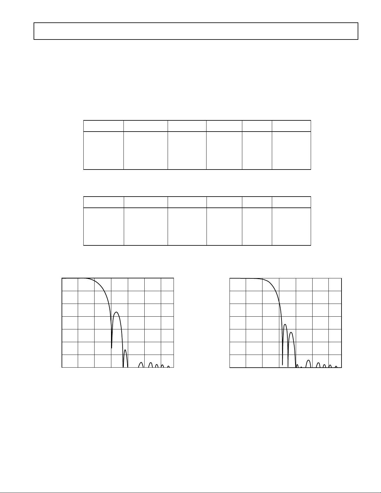
INTERNAL FILTER RESPONSE
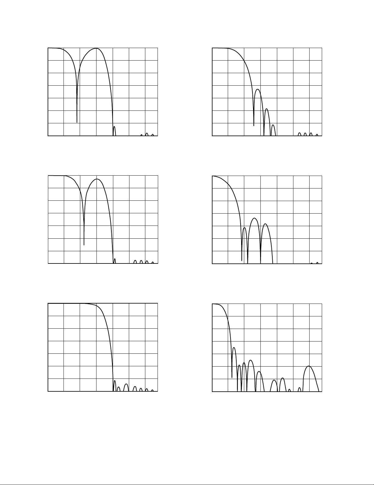
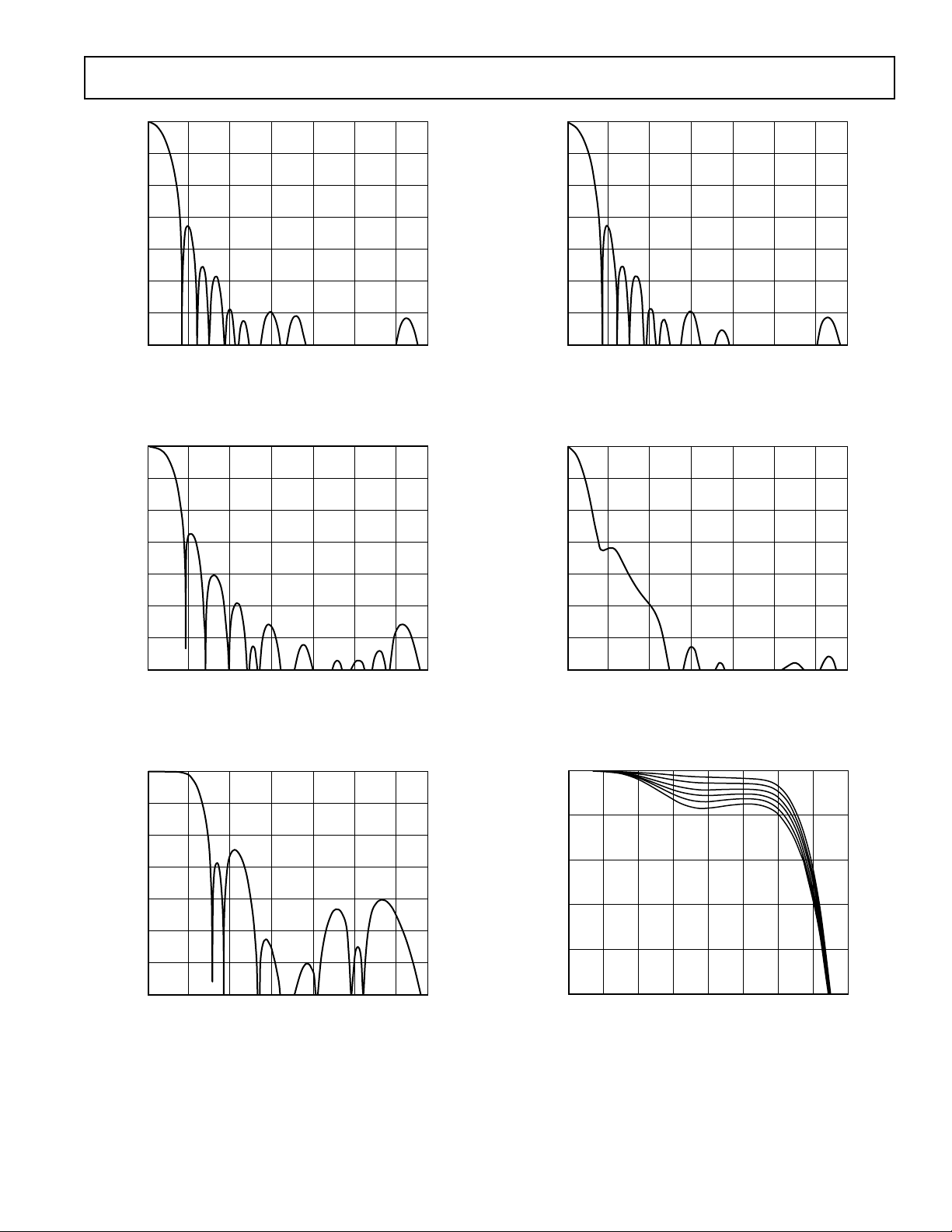
The Y Filter supports several different frequency responses,
including two low-pass responses, two notch responses, an Extended (SSAF) response with or without gain boost/attenuation, a
CIF response and a QCIF response. The UV Filter supports
several different frequency responses, including four low-pass
responses, a CIF response and a QCIF response. These can be
seen in Figures 4 to 18.
ADV7172/ADV7173
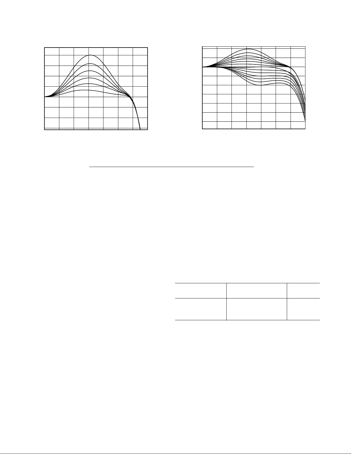
In Extended Mode there is the option of twelve responses in the
range from –4 dB to +4 dB. The desired response can be
chosen by the user by programming the correct value via the
2
C. The variation of frequency responses can be seen in
I
Figures 19 to 21.
–10
–20
FILTER TYPE FILTER SELECTION
MR04
MR03
0
LOW-PASS (NTSC)
LOW-PASS (PAL)
NOTCH (NTSC)
NOTCH (PAL)
EXTENDED (SSAF)
CIF
QCIF
0
0
0
0
1
0
1
1
0
1
0
1
1
PASSBAND RIPPLE
MR02
0
1
0
1
0
1
0
(dB)
0.091
0.15
0.015
0.095
0.051
0.018
MONOTONIC
3 dB BANDWIDTH
(MHz)
4.157
4.74
6.54
6.24
6.217
3.0
1.5
STOPBAND
CUTOFF (MHz)
7.37
7.96
8.3
8.0
8.0
7.06
7.15
STOPBAND
ATTENUATION (dB)
–56
–64
–68
–66
–61
–61
–50
Figure 4. Luminance Internal Filter Specifications
FILTER TYPE FILTER SELECTION
MR07
MR06
0
1.3 MHz LOW PASS
0.65 MHz LOW PASS
1.0 MHz LOW PASS
2.0 MHz LOW PASS
RESERVED
CIF
QCIF
0
0
0
0
1
0
1
1
0
1
0
1
1
PASSBAND RIPPLE
MR05
0
1
0
1
0
1
0
(dB)
0.084
MONOTONIC
MONOTONIC
0.0645
0.084
MONOTONIC
3 dB BANDWIDTH
(MHz)
1.395
0.65
1.0
2.2
0.7
0.5
STOPBAND
CUTOFF (MHz)
3.01
3.64
3.73
5.0
3.01
4.08
STOPBAND
ATTENUATION (dB)
–45
–58.5
–49
–40
–45
–50
Figure 5. Chrominance Internal Filter Specifications
0
–30
–40
MAGNITUDE – dB
–50
–60
–70
0122
46810
FREQUENCY – MHz
Figure 6. NTSC Low-Pass Luma Filter
Figure 7. PAL Low-Pass Luma Filter
–11–REV. A
ADV7172/ADV7173
FREQUENCY – MHz
0
0122
MAGNITUDE – dB
46810
–10
–20
–30
–50
–60
–40
–70
14
FREQUENCY – MHz
0
0122
MAGNITUDE – dB
46810
–10
–20
–30
–50
–60
–40
–70
14
FREQUENCY – MHz
0
0122
MAGNITUDE – dB
46810
–10
–20
–30
–50
–60
–40
–70
14
0
–10
–20
–30
–40
MAGNITUDE – dB
–50
–60
–70
0122
46810
FREQUENCY – MHz
Figure 8. NTSC Notch Luma Filter
0
–10
–20
–30
–40
MAGNITUDE – dB
–50
–60
–70
0122
46810
FREQUENCY – MHz
Figure 9. PAL Notch Luma Filter
0
14
Figure 11. CIF Luma Filter
14
Figure 12. QCIF Luma Filter
–10
–20
–30
–40
MAGNITUDE – dB
–50
–60
–70
0122
46810
FREQUENCY – MHz
Figure 10. Extended Mode (SSAF) Luma Filter
14
Figure 13. 1.3 MHz Low-Pass Chroma Filter
–12– REV. A
0
FREQUENCY – MHz
0
0122
MAGNITUDE – dB
46810
–10
–20
–30
–50
–60
–40
–70
14
FREQUENCY – MHz
0
0122
MAGNITUDE – dB
46810
–10
–20
–30
–50
–60
–40
–70
14
FREQUENCY – MHz
612345
8
7
0
MAGNITUDE – dB
–5
–15
–20
–10
–25
0
–10
–20
–30
–40
MAGNITUDE – dB
–50
–60
ADV7172/ADV7173
–70
0122
46810
FREQUENCY – MHz
Figure 14. 0.65 MHz Low-Pass Chroma Filter
0
–10
–20
–30
–40
MAGNITUDE – dB
–50
–60
–70
0122
46810
FREQUENCY – MHz
Figure 15. 1.0 MHz Low-Pass Chroma Filter
0
14
Figure 17. CIF Chroma Filter
14
Figure 18. QCIF Chroma Filter
–10
–20
–30
–40
MAGNITUDE – dB
–50
–60
–70
0122
46810
FREQUENCY – MHz
Figure 16. 2.0 MHz Low-Pass Chroma Filter
14
Figure 19. Extended Mode Luma Filter with Programmable
Gain, Negative Response
–13–REV. A
ADV7172/ADV7173
4
3
2
1
0
AMPLITUDE – dB
–1
–2
–3
0
FREQUENCY – MHz
Figure 20. Extended Mode Luma Filter with Programmable
Gain, Positive Response
7
612345
4
2
0
–2
–4
–6
MAGNITUDE – dB
–8
–10
–12
2345
FREQUENCY – MHz
61
Figure 21. Extended Mode Luma Filter with Programmable
Gain, Combined Response
COLOR BAR GENERATION
The ADV7172/ADV7173 can be configured to generate 75%
amplitude, 75% saturation (75/7.5/75/7.5) for NTSC or 75%
amplitude, 100% saturation (100/0/75/0) for PAL color bars.
These are enabled by setting MR46 of Mode Register 4 to
Logic “1.”
SQUARE PIXEL MODE
The ADV7172/ADV7173 can be used to operate in square pixel
mode. For NTSC operation, an input clock of 24.5454 MHz
is required. Alternatively, for PAL operation, an input clock of
29.5 MHz is required. The internal timing logic adjusts accordingly for square pixel mode operation.
COLOR SIGNAL CONTROL
The color information can be switched on and off the video
output using Bit MR44 of Mode Register 4.
BURST SIGNAL CONTROL
The burst information can be switched on and off the video
output using Bit MR45 of Mode Register 4.
NTSC PEDESTAL CONTROL
The pedestal on both odd and even fields can be controlled on
a line-by-line basis using the NTSC Pedestal Control Registers. This allows the pedestals to be controlled during the
Vertical Blanking Interval (lines 10 to 25 and lines 273 to 288).
COLOR CONTROLS
The ADV7172/ADV7173 allows the user the advantage of controlling the brightness, contrast, hue and saturation of the color.
Contrast Control
Contrast adjustment is achieved by scaling the Y input data
by a factor programmed by the user into the Contrast Control
Register Bits 5–0. This factor allows the data to be scaled
between 75% and 125%.
Brightness Control
The brightness is controlled by adding a programmable setup
level onto the scaled Y data. This brightness level may be added
onto the Y data in PAL mode, NTSC mode without pedestal or
NTSC mode with pedestal, in which case it is added directly
onto the 7.5 IRE pedestal already present.
The level added is programmed by the user into the Brightness
Control Register (Bits 4–0) and the user is capable of adding
from 0 IRE to a maximum of 14 IRE in 32 (2
5
) steps. Because
of different gains in the datapath for each mode, different values
may need to be programmed to obtain the same IRE setup level
in each mode. Maximum brightness is achieved when 31 is
programmed into the Brightness Control Register. Table II
illustrates the maximum setup/brightness amplitudes available in
the various modes. Note that if a level of less than 7.5 IRE is
required on the Y data in NTSC mode, then NTSC without
pedestal must be the mode selected.
Table II. Maximum Brightness Levels Available
Brightness Control
Mode Register Setup
NTSC No Pedestal 00011111 14 IRE
NTSC Pedestal 00011111 13 IRE
PAL 00011111 99 mV
Color Saturation Control
Color adjustment is achieved by scaling the Cr and Cb input
data by a factor programmed by the user into the Color Control
Registers 1 and 2, Bits 5–0. This factor allows the data to be
scaled between 75% and 125%.
Hue Control
The hue adjustment is achieved on the composite and chroma
outputs by adding a phase offset onto the color subcarrier in the
active video but leaving the color burst unmodified, i.e., only
the phase between the video and the color burst is modified
and hence the hue is shifted. Hue adjustment is under the control of the Hue Control Register. The ADV7172/ADV7173
provides a range of ±22° change in increments of 0.17578125°.
–14– REV. A

ADV7172/ADV7173
YUV LEVELS
This functionality is under the control of Mode Register 5, Bits
2–0. Bit 0 (MR50) allows the ADV7172/ADV7173 to output
SMPTE levels on the Y output when configured in NTSC mode,
and Betacam levels on the Y output when configured in PAL
mode and vice-versa.
Video Sync
Betacam 286 mV 714 mV
SMPTE 300 mV 700 mV
As the datapath is branched at the output of the filters, the
luma signal relating to the CVBS or S-Video Y/C output is
unaltered. Only the Y output of the YUV outputs is scaled.
Bits 2–1 (MR52–MR51) allow UV levels to have a peak-peak
amplitude of 700 mV or 1000 mV, or the default values of
934 mV in NTSC and 700 mV in PAL.
AUTODETECT CONTROL
The ADV7172/ADV7173 provides the option of automatically
powering down the DACs A, B and C if they are not correctly
terminated (i.e., the 75 Ω cable is not connected to the DAC).
The voltage at the output of DACs A and B are compared to
a selected reference level. This reference voltage (MR64) will
depend on whether the user terminates with 37.5 Ω (75 Ω connected on the DAC end and 75 Ω connected at TV end of cable,
i.e., combined load of 37.5 Ω) or 75 Ω. It cannot operate in a
DAC buffering configuration. There are two modes of autodetect operation provided by the ADV7172/ADV7173:
(1) Mode 0: The state of termination of the DAC may be read
by reading the status bits in Mode Register 6. MR67 status bit
indicates whether or not the composite DAC is terminated,
MR66 status bit indicates whether or not the luma DAC is
terminated. The user may then decide whether or not to power
down the DACs using MR15–MR0.
(2) Mode 1: The state of the DACs may be read as in Mode 0.
If either of the DACs is unterminated, they are automatically
powered down. If the luma DAC, DAC B is powered down then
DAC C, the chroma DAC, will also be powered down. The
state of termination of the DAC is checked each frame to decide
whether or not it is to be powered up or down.
Mode Register 6, Bits 3–2, indicates which mode of operation is
used. Note that Mode Register 1, Bits 5-3, must be enabled
(“1”) for autodetect functionality to work. (DACs A, B, C are
enabled.)
Vertical Blanking Data Insertion
It is possible to allow encoding of incoming YCbCr data on
those lines of VBI that do not have line sync or pre-/postequalization pulses (see Figures 24 to 25). This mode of operation is called “Partial Blanking” and is selected by setting MR32
to “1.” It allows the insertion of any VBI data (Opened VBI)
into the encoded output waveform. This data is present in digitized incoming YCbCr data stream (e.g., WSS data, CGMS,
VPS etc.). Alternatively the entire VBI may be blanked (no VBI
data inserted) on these lines by setting MR32 to “0.”
The complete VBI comprises of the following lines:
525/60 systems, Lines 525 to 21 for Field 1 and Lines 262 to
Line 284 for Field 2.
625/50 systems, Lines 624 to Line 22 and lines 311 to 335.
The “Opened VBI” consists of:
525/60 systems, Lines 10 to 21 for Field 1 and second half of
Line 273 to Line 284 for Field 2.
625/50 systems, Line 7 to Line 22 and Lines 319 to 335.
SUBCARRIER RESET
Together with the SCRESET/RTC PIN and Bits MR42 and
MR41 of Mode Register 4, the ADV7172/ADV7173 can be
used in subcarrier reset mode. The subcarrier phase will reset
to Field 0 at the start of the following field when a low to high
transition occurs on this input pin.
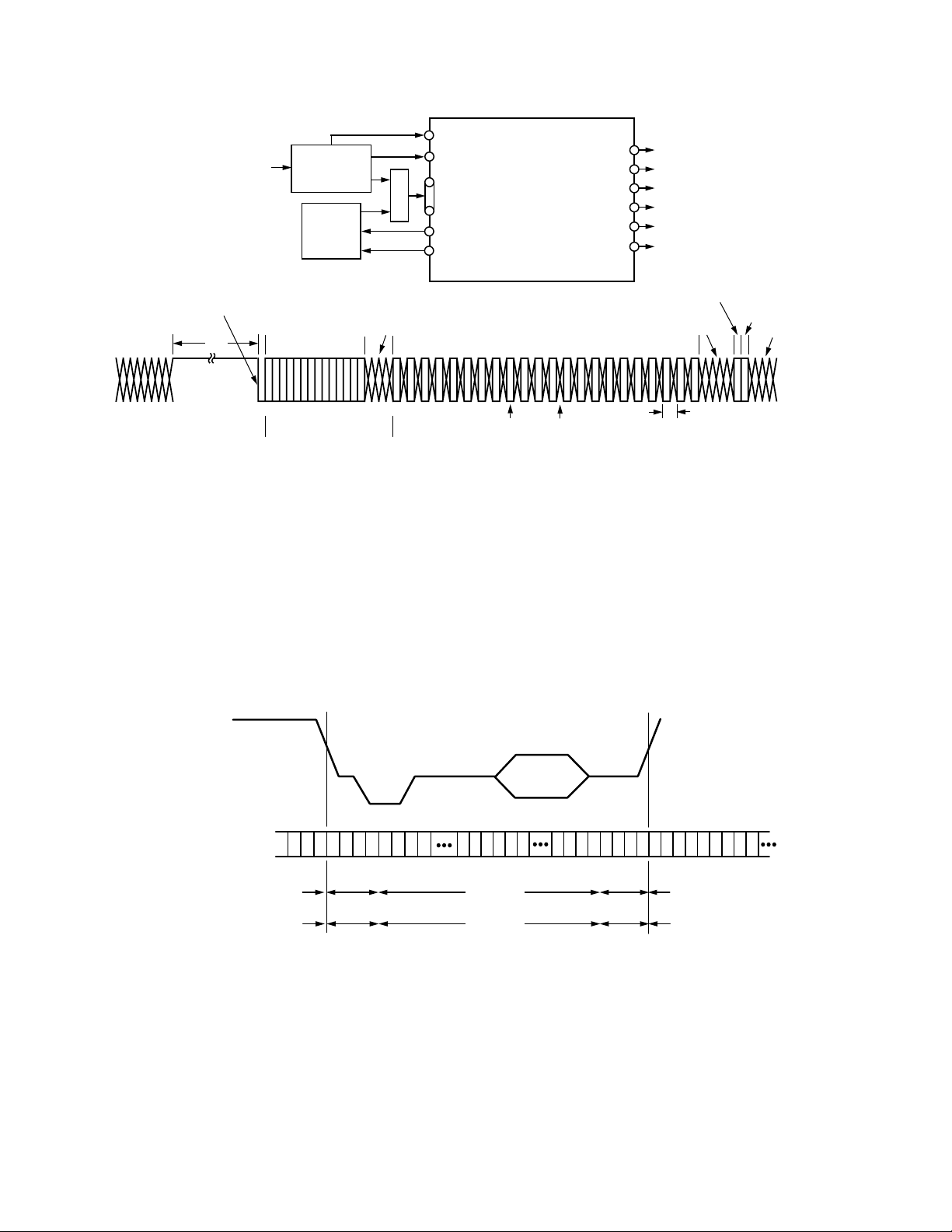
REAL-TIME CONTROL
Together with the SCRESET/RTC PIN and Bits MR42 and
MR41 of Mode Register 4, the ADV7172/ADV7173 can be
used to lock to an external video source. The real-time control
mode allows the ADV7172/ADV7173 to automatically alter the
subcarrier frequency to compensate for line length variation.
When the part is connected to a device that outputs a digital
data stream in the RTC format (such as a ADV7185 video
decoder, see Figure 22), the part will automatically change to
the compensated subcarrier frequency on a line-by-line basis.
This digital data stream is 67 bits wide and the subcarrier is
contained in Bits 0 to 21. Each bit is two clock cycles long.
00Hex should be written into all four subcarrier frequency
registers when using this mode.
VIDEO TIMING DESCRIPTION
The ADV7172/ADV7173 is intended to interface to off-theshelf MPEG1 and MPEG2 Decoders. As a consequence, the
ADV7172/ADV7173 accepts 4:2:2 YCrCb Pixel Data via a
CCIR-656 pixel port and has several video timing modes of
operation that allow it to be configured as either system master
video timing generator or a slave to the system video timing
generator. The ADV7172/ADV7173 generates all of the required horizontal and vertical timing periods and levels for the
analog video outputs.
The ADV7172/ADV7173 calculates the width and placement
of analog sync pulses, blanking levels and color burst envelopes.
Color bursts are disabled on appropriate lines and serration and
equalization pulses are inserted where required.
In addition, the ADV7172/ADV7173 supports a PAL or NTSC
square pixel operation in slave mode. The part requires an
input pixel clock of 24.5454 MHz for NTSC and an input pixel
clock of 29.5 MHz for PAL. The internal horizontal line counters
place the various video waveform sections in the correct location for the new clock frequencies.
The ADV7172/ADV7173 has four distinct master and four
distinct slave timing configurations. Timing control is established with the bidirectional SYNC, BLANK and FIELD/
VSYNC pins. Timing Mode Register 1 can also be used to
vary the timing pulsewidths and where they occur in relation to
each other.
–15–REV. A
ADV7172/ADV7173
COMPOSITE
OR CABLE
H/LTRANSITION
COUNT START
128
RTC
TIME SLOT: 01
NOTES:
1
FSC PLL INCREMENT IS 22 BITS LONG, VALUE LOADED INTO ADV7172/ADV7173 FSC DDS REGISTER IS FSC PLL INCREMENT BITS 21:0 PLUS BITS 0:9
OF SUBCARRIER FREQUENCY REGISTERS. ALL ZEROS SHOULD BE WRITTEN TO THE SUBCARRIER FREQUENCY REGISTERS OF THE
ADV7172/ADV7173.
2
SEQUENCE BIT
PAL: 0 = LINE NORMAL, 1 = LINE INVERTED
NTSC: 0 = NO CHANGE
3
RESET BIT
RESET ADV7172/ADV7173’s DDS
VIDEO
e.g., VCR
LOW
VIDEO
DECODER
(e.g., ADV7185)
MPEG
DECODER
14 BITS
RESERVED
NOT USED IN
ADV7172/ADV7173
14
4 BITS
RESERVED
013
CLOCK
GREEN/COMPOSITE/Y
BLUE/LUMA/U
RED/CHROMA/V
GREEN/COMPOSITE/Y
BLUE/LUMA/U
RED/CHROMA/V
M
U
X
SCRESET/RTC
P7–P0
HSYNC
FIELD/VSYNC
ADV7172/ADV7173
SEQUENCE
2
BIT
RESET
3
5 BITS
21
19
FSCPLL INCREMENT
VALID
SAMPLE
SAMPLE
1
INVALID
RESERVED
0
8/LLC
BIT
RESERVED
67 68
Figure 22. RTC Timing and Connections
Mode 0 (CCIR–656): Slave Option
(Timing Register 0 TR0 = X X X X X 0 0 0)
The ADV7172/ADV7173 is controlled by the SAV (Start Active Video) and EAV (End Active Video) Time Codes in the Pixel Data.
All timing information is transmitted using a 4-byte Synchronization Pattern. A synchronization pattern is sent immediately before
and after each line during active picture and retrace. Mode 0 is illustrated in Figure 23. The HSYNC, FIELD/VSYNC and BLANK
(if not used) pins should be tied high during this mode.
ANALOG
VIDEO
INPUT PIXELS
NTSC/PAL M SYSTEM
(525 LlNES/60Hz)
PAL SYSTEM
(625 LINES/50Hz)
EAV CODE
000
C
F
Y
Y
r
F
4 CLOCK
4 CLOCK
END OF ACTIVE
VIDEO LINE
10801
XY8
0
0
0
FF00FFABABA
ANCILLARY DATA
268 CLOCK
280 CLOCK
B
(HANC)
801
0
SAV CODE
10FF0
8
0
C
X
0
Y
0
b
VIDEO LINE
Y
0
4 CLOCK
4 CLOCK
START OF ACTIVE
C
C
Y
Y
b
r
1440 CLOCK
1440 CLOCK
C
C
Y
b
r
Figure 23. Timing Mode 0 (Slave Mode)
–16– REV. A
ADV7172/ADV7173
Mode 0 (CCIR–656): Master Option
(Timing Register 0 TR0 = X X X X X 0 0 1)
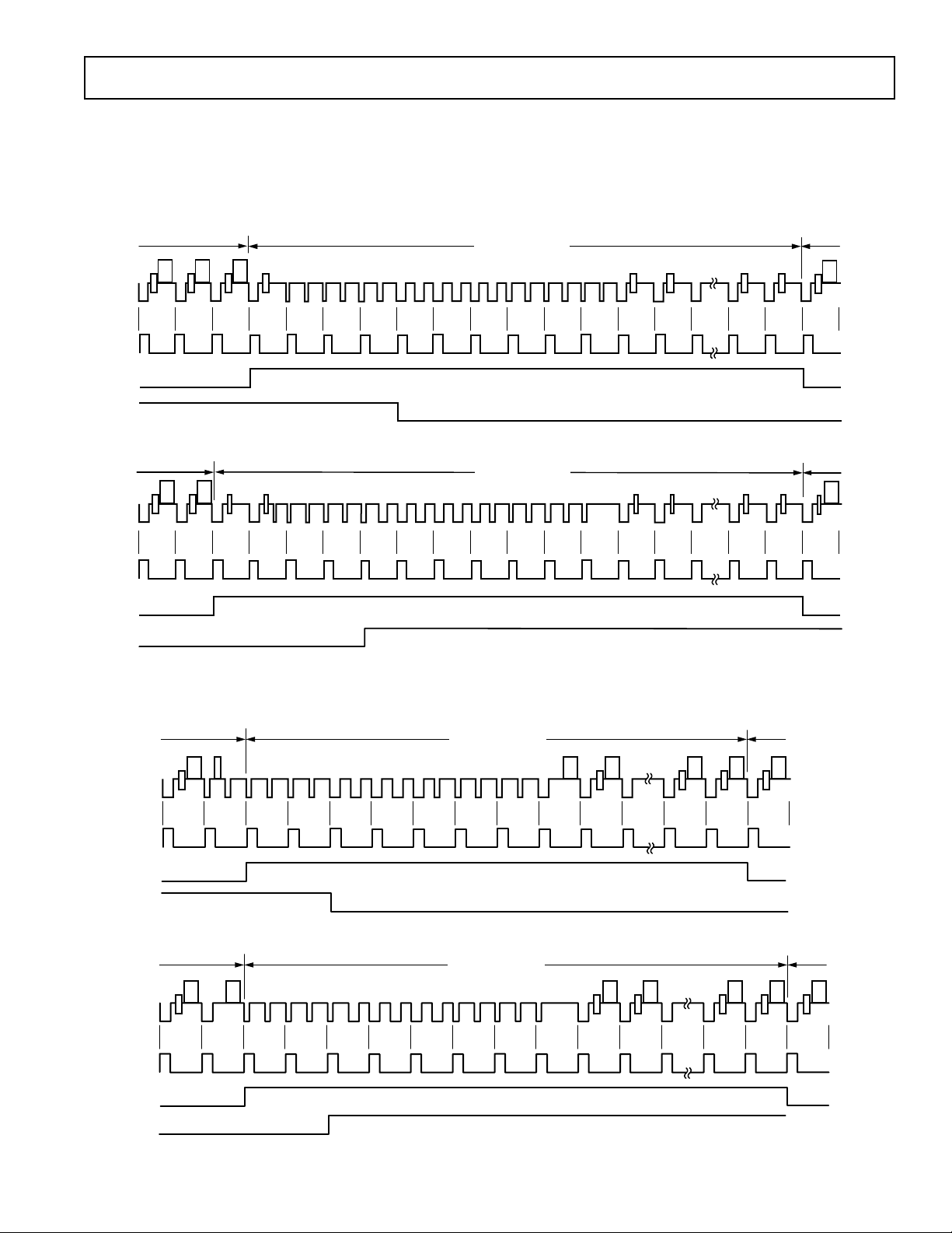
The ADV7172/ADV7173 generates H, V and F signals required for the SAV (Start Active Video) and EAV (End Active Video)
Time Codes in the CCIR656 standard. The H bit is output on the HSYNC pin, the V bit is output on the BLANK pin and the F bit
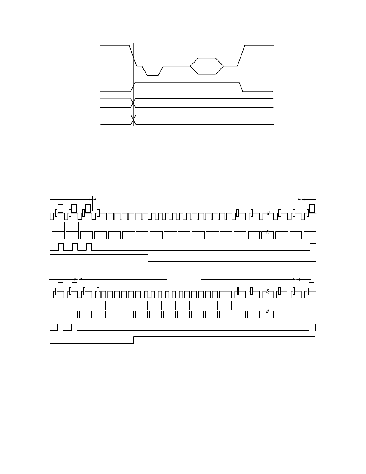
is output on the FIELD/VSYNC pin. Mode 0 is illustrated in Figure 24 (NTSC) and Figure 25 (PAL). The H, V and F transitions
relative to the video waveform are illustrated in Figure 26.
DISPLAY DISPLAY
VERTICAL BLANK
522 523 524 525 1 2 3 4
5
67
9
8
H
V
F
DISPLAY
260 261 262 263 264 265 266 267 268 269 270 271 272 273 274
EVEN FIELD
ODD FIELD
VERTICAL BLANK
H
V
F
ODD FIELD
EVEN FIELD
Figure 24. Timing Mode 0 (NTSC Master Mode)
DISPLAY
VERTICAL BLANK
10 11 20 21 22
DISPLAY
283
DISPLAY
284
285
622 623 624 625 1 2 3 4
H
V
F
DISPLAY
309 310 311 312 314 315 316 317
ODD FIELDEVEN FIELD
313
H
V
F
ODD FIELD EVEN FIELD
Figure 25. Timing Mode 0 (PAL Master Mode)
5
VERTICAL BLANK
–17–REV. A
67
318
319 320
22 23
21
DISPLAY
335 336
334
ADV7172/ADV7173
ANALOG
VIDEO
H
F
V
Figure 26. Timing Mode 0 Data Transitions (Master Mode)
Mode 1: Slave Option HSYNC, BLANK, FIELD
(Timing Register 0 TR0 = X X X X X 0 1 0)
In this mode the ADV7172/ADV7173 accepts horizontal SYNC and Odd/ Even FIELD signals. A transition of the FIELD input
when HSYNC is low indicates a new frame, i.e., Vertical Retrace. The BLANK signal is optional. When the BLANK input is dis-
abled, the ADV7172/ADV7173 automatically blanks all normally blank lines as per CCIR-624. Mode 1 is illustrated in Figure 27
(NTSC) and Figure 28 (PAL).
HSYNC
BLANK
FIELD
HSYNC
BLANK
FIELD
284
DISPLAY
285
DISPLAY
522 523 524 525
DISPLAY DISPLAY
260 261 262 263 264 265 266 267 268 269 270 271 272 273 274
1234
ODD FIELDEVEN FIELD
ODD FIELD EVEN FIELD
VERTICAL BLANK
678
5
VERTICAL BLANK
10 11
9
20 21 22
283
Figure 27. Timing Mode 1 (NTSC)
–18– REV. A
 Loading...