Analog Devices ADV7162KS140, ADV7160KS220, ADV7160KS170, ADV7160KS140, ADV7162KS220 Datasheet
...
96-Bit, 220 MHz
a
FEATURES
96-Bit Pixel Port for 1600 × 1280 × 24 Screen Resolution
220 MHz, 24-Bit (30-Bit Gamma Corrected) True-Color
Triple 10-Bit “Gamma Correcting” D/A Converters
2% (max) DAC to DAC Color Matching
Triple 256 × 10 (256 x 30) Color Palette RAM
On-Board User Definable Cursor (64 × 64 × 2)
Three Color Overlay
Cursor Palette RAM
Fully Programmable On-Board PLL
RS-343A/RS-170 Compatible RGB Analog Outputs
Tri-Level SYNC Functionality
TTL Compatible Digital Inputs
Standard MPU I/O Interface
Programmable Pixel Port: 24-Bit, 16-Bit, 15-Bit &
8-Bit (Pseudo)
Pixel Data Serializer:
Multiplexed Pixel Input Ports; 2:1, 4:1, 8:1
+5 V CMOS Monolithic Construction
160-Lead Plastic Quad Flatpack (QFP): ADV7162
160-Lead “Thermally Enhanced” QFP (PQUAD): ADV7160
ADV is a registered trademark of Analog Devices, Inc.
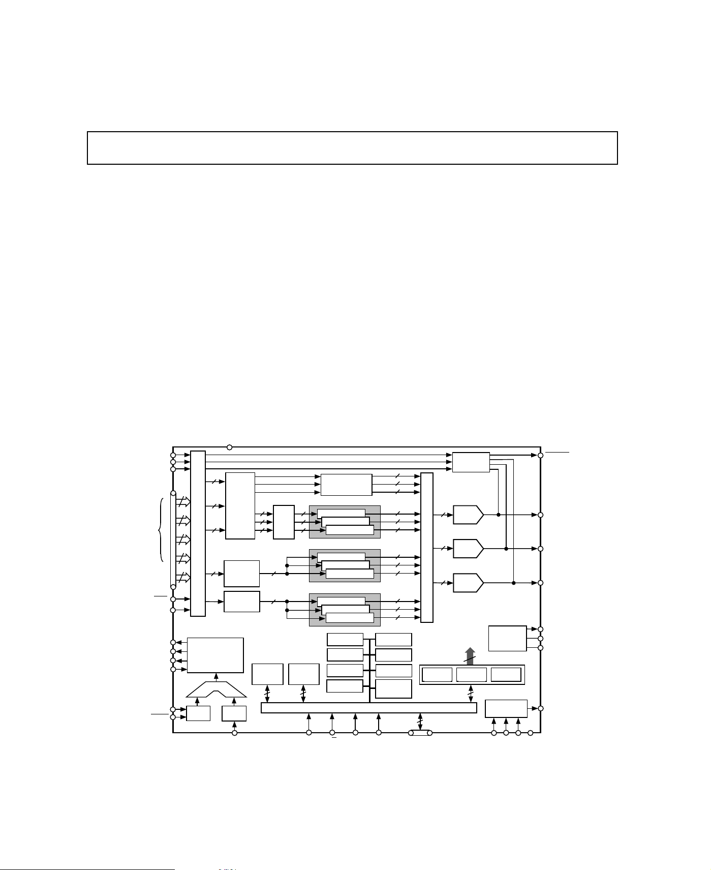
FUNCTIONAL BLOCK DIAGRAM
3 x 256 COLOR PALETTE
2
2
10
8
8
PIXEL
MASK
8
3 COLOR OVERLAY PALETTE
2 COLOR CURSOR PALETTE
CONTROL
REGISTERS
MODE
REGISTER
(MR1)
10
8
8
8
ADDRESS
REGISTER
(A10-A0)
TRISYNC
SYNC
BLANK
PIXEL
DATA
(P7-P0)
PALETTE
SELECTS
(PS0, PS1)
ODD/EVEN
LOADIN
LOADOUT
PRGCKOUT
SCKOUT
SCKIN
CLOCK
CLOCK
24
A
24
B
24
C
24
D
8
V
AA
P
I
X
8
E
L
I
8
N
P
U
T
8
M
U
L
T
I
2
P
L
E
X
E
R
CLOCK CONTROL
CLOCK DIVIDE &
SYNCHRONIZATION
÷32, ÷16, ÷8, ÷4
ECL TO
CMOS
FUNCTION
GENERATOR
CIRCUITRY
SELECTOR
PLL
COLOR
MODE
MATRIX
PS
DECODE
LOGIC
64 x 64
CURSOR
BYPASS COLOR
MODE MATRIX
RED 256 x 10
GREEN 256 x 10
BLUE 256 x 10
RED 3 x 10
GREEN 3 x 10
BLUE 3 x 10
RED 3 x 10
GREEN 3 x 10
BLUE 3 x 10
CURSOR
REGISTERS
TEST
REGISTERS
ID
REGISTER
STATUS
REGISTER
True-Color Video RAM-DAC
ADV7160/ADV7162
MODES OF OPERATION
1600 × 1200 × 30/24-Bit Resolution @ 85 Hz Screen Refresh
1600 × 1200 × 16/15-Bit Resolution @ 85 Hz Screen Refresh
1600 × 1200 × 8-Bit Resolution @ 85 Hz Screen Refresh
APPLICATIONS
Windows Accelerators
High Resolution, True Color Graphics
Professional Color Prepress Imaging
Digital TV (HDTV, Digital Video)
SPEED GRADES
@ 220 MHz
@ 170 MHz
@ 140 MHz
GENERAL DESCRIPTION
The ADV7160/ADV7162® is a 96-bit pixel port Video RAMDAC with color enhanced triple 10-bit DACs. The device also
includes a PLL and 64 × 64 hardware cursor. The ADV7160/
ADV7162 is specifically designed for use in the graphics subsystem of high performance, color graphics workstations and
windows accelerators.
(Continued on page 15)
SYNCOUT
IOR
IOG
IOB
V
REF
R
SET
COMP
TDO
MPU PORT
10
10
10
10
10
10
10
10
10
10
10
10
PIXEL MASK
REGISTER
REVISION
REGISTER
PLL
REGISTERS
COMMAND
REGISTERS
(CR1-CR5)
10
S
E
L
10
E
C
T
O
R
10
DATA TO
PALETTES
RED
REGISTER
10 (8+2)
BLANK AND
SYNC LOGIC
RED
DAC
GREEN
DAC
BLUE
DAC
ADV7160/
ADV7162
30
GREEN
REGISTER
10
VOLTAGE
REFERENCE
CIRCUIT
BLUE
REGISTER
JTAG TEST
ACCESS PORT
PLL
REF
R/W
C1
REV. 0
Information furnished by Analog Devices is believed to be accurate and
reliable. However, no responsibility is assumed by Analog Devices for its
use, nor for any infringements of patents or other rights of third parties
which may result from its use. No license is granted by implication or
otherwise under any patent or patent rights of Analog Devices.
CE
D9–D0C0
TCKTMS
GNDTDI
© Analog Devices, Inc., 1995
One Technology Way, P.O. Box 9106, Norwood. MA 02062-9106, U.S.A.
Tel: 617/329-4700 Fax: 617/326-8703

1
(V
ADV7160/ADV7162–SPECIFICATIONS
= +5 V; V
AA
C
= 10 pF). All specifications T
L
= +1.235 V; R
REF
= 280 Ω. IOR, IOG, IOB (RL = 37.5 Ω,
SET
MIN
2
to T
unless otherwise noted.)
MAX
Parameter Min Typ Max Units Test Conditions/Comments
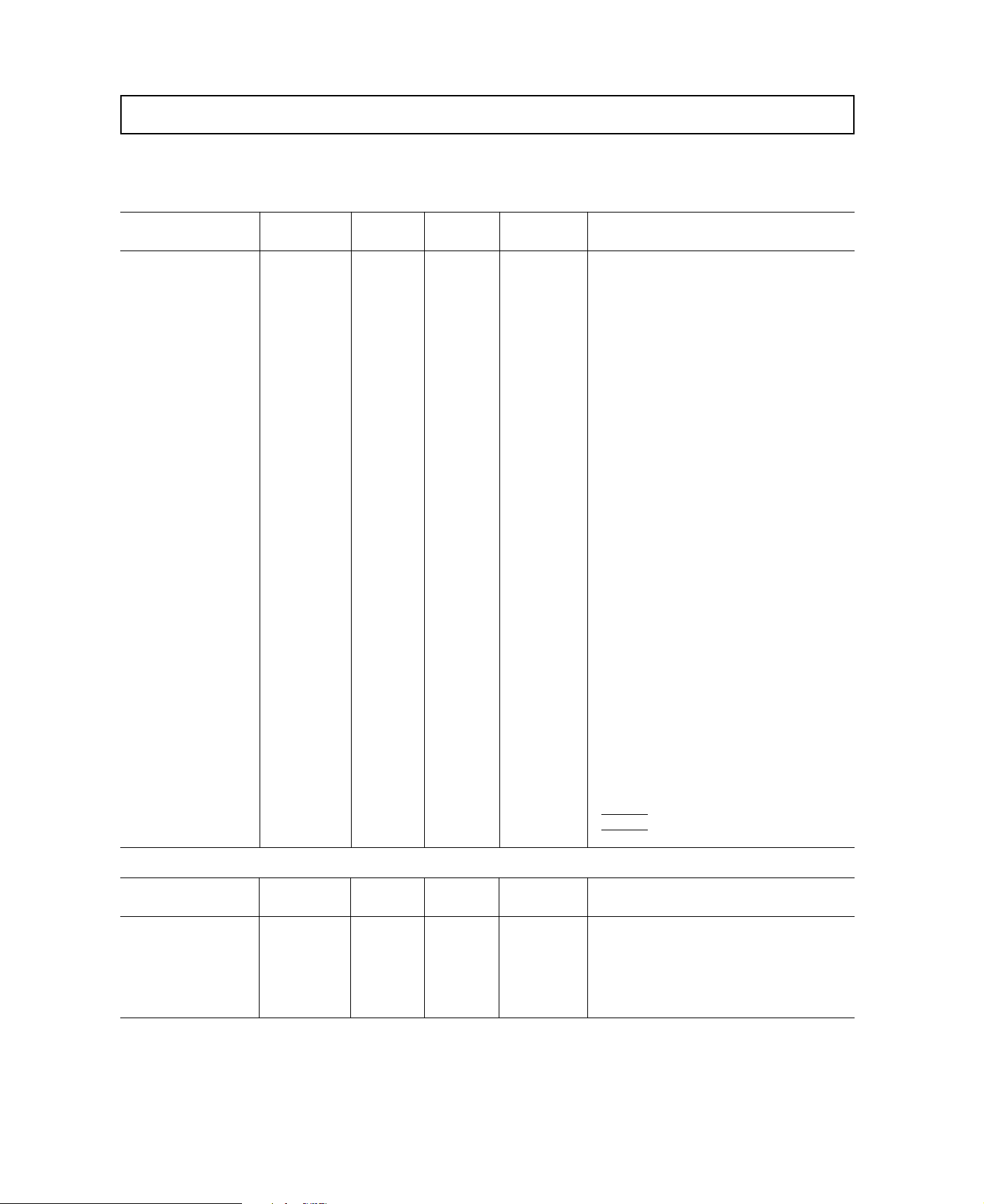
STATIC PERFORMANCE (DAC Gain Setting = 3996)
Resolution (Each DAC) 10 Bits
Accuracy (Each DAC)
Integral Nonlinearity ±1 LSB
Differential Nonlinearity ± 1 LSB Guaranteed Monotonic
Gray Scale Error ±5 % Gray Scale
Coding Binary
DIGITAL INPUTS
Input High Voltage, V
Input Low Voltage, V
Input Current, I
Input Capacitance, C
CLOCK INPUTS (CLOCK,
Input High Voltage, V
Input Low Voltage, V
Input Current, I
Input Current, I
Input Capacitance, C
INH
INL
IN
IN
CLOCK)
INH
INL
IN
(JTAG Inputs) ±50 µAV
IN
IN
2V
0.8 V
±10 µAV
= 0.4 V or 2.4 V
IN
10 pF
VAA – 1.0 V
VAA – 1.6 V
±10 µAV
= 0.4 V or 2.4 V
IN
= 0.4 V or 2.4 V
IN
10 pF
DIGITAL OUTPUTS
Output High Voltage, V
Output Low Voltage, V
OL
OH
2.4 V I
0.4 V I
SOURCE
= 3.2 mA
SINK
= 400 µA
Floating-State Leakage Current 20 µA
Floating-State Output Capacitance 20 pF
ANALOG OUTPUTS (DAC Gain Setting = 3996)
Gray Scale Current Range 15 22 mA
Output Current
White Level Relative to Blank 17.69 19.05 20.40 mA
White Level Relative to Black 16.74 17.62 18.50 mA
Black Level Relative to Blank 0.95 1.44 1.90 mA
Blank Level 0 5 50 µA Sync Disabled
Blank Level 6.29 7.62 8.96 mA Sync Enabled
Sync Level 0 5 50 µA
Tri-Sync Level Relative to Blank 6.29 7.62 8.96 mA
LSB Size 17.22 µA
DAC to DAC Matching 1 3 %
Output Compliance, V
Output Impedance, R
OC
OUT
Output Capacitance, C
OUT
0 +1.4 V
30 kΩ
30 pF I
OUT
= 0 mA
VOLTAGE REFERENCE
Voltage Reference Range, V
Input Current, I
VREF
REF
1.14 1.235 1.26 V V
5 µA
= 1.235 V for Specified Performance
REF
POWER REQUIREMENTS
V
AA
3
I
AA
5V
475 mA For 220 MHz Operation (ADV7160)
440 mA For 170 MHz Operation (ADV7160)
3
I
AA
410 mA For 140 MHz Operation (ADV7160)
450 mA For 220 MHz Operation (ADV7162)
400 mA For 170 MHz Operation (ADV7162)
360 mA For 140 MHz Operation (ADV7162)
Power Supply Rejection Ratio 0.1 %/% COMP = 0.1 µF
DYNAMIC PERFORMANCE
Clock and Data Feedthrough
Glitch Impulse 50 pV secs
DAC to DAC Crosstalk
NOTES
1
±5% for all versions.
2
Temperature range (T
3
Pixel Port is continuously clocked with data corresponding to a linear ramp. TJ = 100oC.
4
Clock and data feedthrough is a function of the amount of overshoot and undershoot on the digital inputs. Glitch impulse includes clock and data feedthrough.
5
TTL input values are 0 V to 3 V, with input rise/fall times ≤3 ns, measured the 10% and 90% points. Timing reference points at 50% for inputs and outputs.
6
DAC to DAC Crosstalk is measured by holding one DAC high while the other two are making low to high and high to low transitions.
Specifications subject to change without notice.
MIN
to T
4, 5
6
): 0°C to +70°C.
MAX
–30 dB
–23 dB
–2–
REV. 0
ADV7160/ADV7162
2
(V
= +5 V; V
AA
TIMING CHARACTERISTICS
CLOCK CONTROL AND PIXEL PORT
1
specifications T
4
Parameter 220 MHz 170 MHz 140 MHz Units Conditions/Comments
Version Version Version
= +1.235 V; R
REF
to T
MIN
MAX
= 280 Ω. IOR, IOG, IOB (RL = 37.5 Ω, CL = 10 pF). All
SET
3
unless otherwise noted.)
f
CLOCK
t
1
t
2
t
3
t
4
f
LOADIN
220 170 140 MHz max Pixel CLOCK Rate
4.5 5.88 7.14 ns min Pixel CLOCK Cycle Time
2.0 2.5 2.86 ns min Pixel CLOCK High Time
2.0 2.5 2.86 ns min Pixel CLOCK Low Time
10 10 10 ns max Pixel CLOCK to LOADOUT Delay
2:1 Multiplexing 110 85 70 MHz max
4:1 Multiplexing 55 42.5 35 MHz max
8:1 Multiplexing 27.5 21.25 17.5 MHz max
t
5
2:1 Multiplexing 9.1 11.77 14.29 ns min
4:1 Multiplexing 18.18 23.53 28.58 ns min
8:1 Multiplexing 36.36 47.1 57.16 ns min
t
6
2:1 Multiplexing 4 5 6 ns min
4:1 Multiplexing 8 9 12 ns min
8:1 Multiplexing 15 18 23 ns min
t
7
2:1 Multiplexing 4 5 6 ns min
4:1 Multiplexing 8 9 12 ns min
8:1 Multiplexing 15 18 23 ns min
t
8
t
9
0 0 0 ns min Pixel Data Setup Time
5 5 5 ns min Pixel Data Hold Time
LOADIN Clocking Rate
LOADIN Cycle Time
LOADIN High Time
LOADIN Low Time
t
10
5
τ-t
11
6
t
PD
2:1 Multiplexing 9 9 9 CLOCKs (1 × CLOCK = t
0 0 0 ns min LOADOUT to LOADIN Delay
τ-5 τ-5 τ-5 ns max LOADOUT to LOADIN Delay
Pipeline Delay
)
1
4:1 Multiplexing 11 11 11 CLOCKs
8:1 Multiplexing 15 15 15 CLOCKs
t
12
t
13
t
14
t
15
ANALOG OUTPUTS
7
10 10 10 ns max Pixel CLOCK to PRGCKOUT Delay
5 5 5 ns max SCKIN to SCKOUT Delay
5 5 5 ns min BLANK to SCKIN Setup Time
0 0 0 ns min BLANK to SCKIN Hold Time
Parameter 220 MHz 170 MHz 140 MHz Units Conditions/Comments
Version Version Version
t
16
t
17
t
18
t
SK
25 25 25 ns typ Analog Output Delay
1 1 1 ns typ Analog Output Rise/Fall Time
25 25 25 ns typ Analog Output Transition Time
2 2 2 ns max RGB Analog Output Skew
0 0 0 ns typ
REV. 0
–3–
ADV7160/ADV7162
ORT
8,9
MPU P
Parameter 220 MHz 170 MHz 140 MHz Units Conditions/Comments
Version Version Version
t
19
t
20
t
21
t
22
8
t
23
9
t
24
9
t
25
9
t
26
t
27
t
28
NOTES
General Notes
1
TTL input values are 0 to 3 volts, with input rise/fall times ≤ 3 ns, measured between the 10% and 90% points.
ECL inputs (CLOCK,
Timing reference points at 50% for inputs and outputs.
Analog output load ≤ 10 pF.
Data-Bus (D0–D9) loaded as shown in Figure 1.
Digital output load for LOADOUT, PRGCKOUT & SCKOUT ≤ 30 pF.
2
±5% for all versions
3
Temperature range (T
Notes on PIXEL PORT
4
Pixel Port consists of the following inputs:
Pixel Inputs: RED [A, B, C, D] GREEN [A, B, C, D] BLUE [A, B, C, D]
Palette Selects: PS0 [A, B, C, D]; PS1[A, B, C, D]
Pixel Controls:
Clock Inputs: CLOCK,
Clock Outputs: LOADOUT, PRGCKOUT, SCKOUT
5
τ is the LOADOUT Cycle Time and is a function of the Pixel CLOCK Rate and the Multiplexing Mode:
2:1 multiplexing; τ = CLOCK × 2= 2 × t
4:1 multiplexing; τ = CLOCK × 4= 4 × t
8:1 multiplexing; τ = CLOCK × 8= 8 × t1ns
6
These fixed values for Pipeline Delay are valid under conditions where t10 and τ-t11 are met. If either t10 or τ-t11 are not met, the part will operate but the Pipeline
Delay is increased.
Notes on ANALOG OUTPUTS
7
Output delay measured from the 50% point of the rising edge of CLOCK to the 50% point of full-scale transition.
Output rise/fall time measured between the 10% and 90% points of full-scale transition.
Transition time measured from the 50% point of full scale transition to the output remaining within 2% of the final output value. (Transition time does not include
clock and data feedthrough).
Notes on MPU PORT
8
t23 and t
9
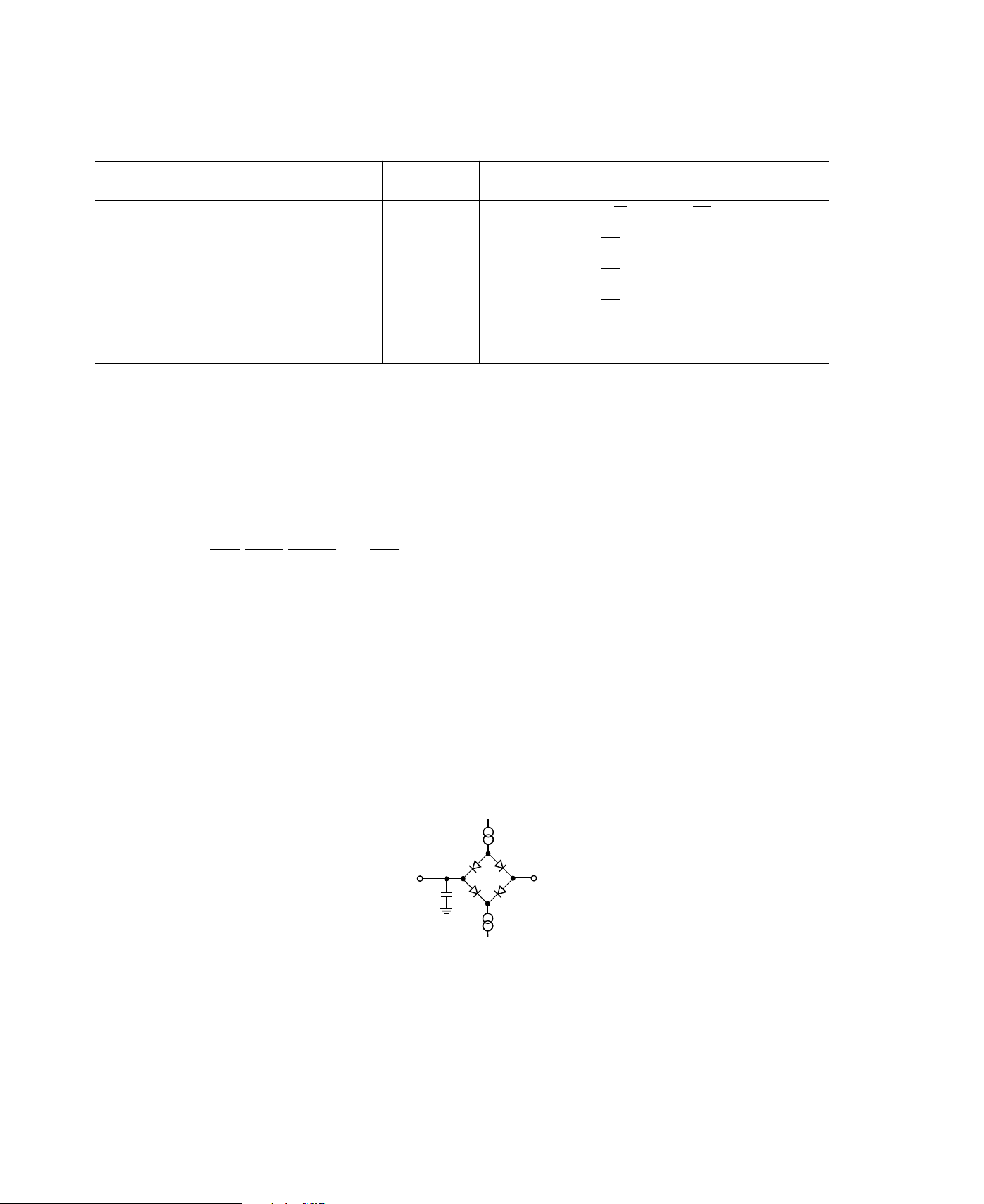
t25 and t26 are derived from the measured time taken by the data outputs to change by 0.5 V when loaded with the circuit of Figure 1. The measured numbers are
are measured with the load circuit of Figure 1 and defined as the time required for an output to cross 0.4 V or 2.4 V.
24
then extrapolated back to remove the effects of charging the 100 pF capacitor. This means that the times t
true values for the device and as such are independent of external loading capacitances.
Specifications subject to change without notice.
0 0 0 ns min R/W, C0, C1 to CE Setup Time
10 10 10 ns min R/W, C0, C1 to CE Hold Time
45 45 45 ns min CE Low Time
25 25 25 ns min CE High Time
5 5 5 ns min CE Asserted to Data-Bus Driven
45 45 45 ns max CE Asserted to Data Valid
20 20 20 ns max CE Disabled to Data-Bus Three-Stated
5 5 5 ns min CE Disabled to Data Invalid
20 20 20 ns min Write Data (D0–D9) Setup Time
5 5 5 ns min Write Data (D0–D9) Hold Time
CLOCK) are VAA–0.8 V to VAA–1.8 V, with input rise/fall times ≤ 2 ns, measured between the 10% and 90% points.
to T
MIN
SYNC, BLANK, TRISYNC, ODD/EVEN
); 0°C to +70°C.
MAX
CLOCK, LOADIN, SCKIN
ns
1
ns
1
and t26, quoted in the Timing Characteristics are the
25
I
SINK
TO OUTPUT
PIN
100pF
I
+2.1V
SOURCE
Figure 1. Load Circuit for Databus Access and Relinquish Times
–4–
REV. 0
TIMING CHARACTERISTICS (Cont.)
2
(V
= +5 V; V
AA
1
All specifications T
= +1.235 V; R
REF
to T
MIN
ADV7160/ADV7162
= 280 Ω. IOR, IOG, IOB (RL = 37.5 Ω, CL =10 pF).
SET
3
unless otherwise noted.)
MAX
JTAG P
ORT
Parameter All Versions Units Conditions/Comments
PLL PERFORMANCE
4
Jitter 250 ps rms 1σ
PLL REFERENCE INPUT
PLL
Frequency 900 kHz min
REF
40 MHz max
V
IH
V
IL
PLL
Period 25 ns min
REF
2.0 V max
0.8 V min
1.67 µs max
PLL
Duty Cycle 40 % min
REF
60 % max
JTAG PERFORMANCE
TCK Frequency, t
TCK High Time, t
TCK Low Time, t
TDI, TMS Setup Time, t
TDI, TMS Hold Time, t
Digital Input to
Digital Input to
TCLK to TDO Drive, t
TCLK to TDO Valid, t
TCLK to TDO Three-State, t
29
30
31
32
33
TCK Setup Time, t
TCK Hold Time, t
36
37
38
34
35
20 MHz max
15 ns min
15 ns min
15 ns max
15 ns max
15 ns max
15 ns max
0 ns min
20 ns min
5 ns min
15 ns max
NOTES
1
TTL input values are 0 to 3 volts, with input rise/fall times ≤ 3 ns, measured between the 10% and 90% points. Timing reference points at 50% for inputs and outputs.
2
±5% for all versions.
3
Temperature range (T
4
Jitter is measured by triggering on the output clock, delayed by 15 µs and then measuring the time period from the trigger edge to the next edge of the output clock
after the delay. This measurement is repeated multiple times and the RMS value is determined.
Specifications subject to change without notice.
MIN
to T
MAX
); 0°C to +70°C.
TCK
TMS, TDI
DIGITAL
INPUT
TDO
TDO
t
t
32
t
34
t
30
t
33
t
35
29
t
31
t
37
t
36
t
38
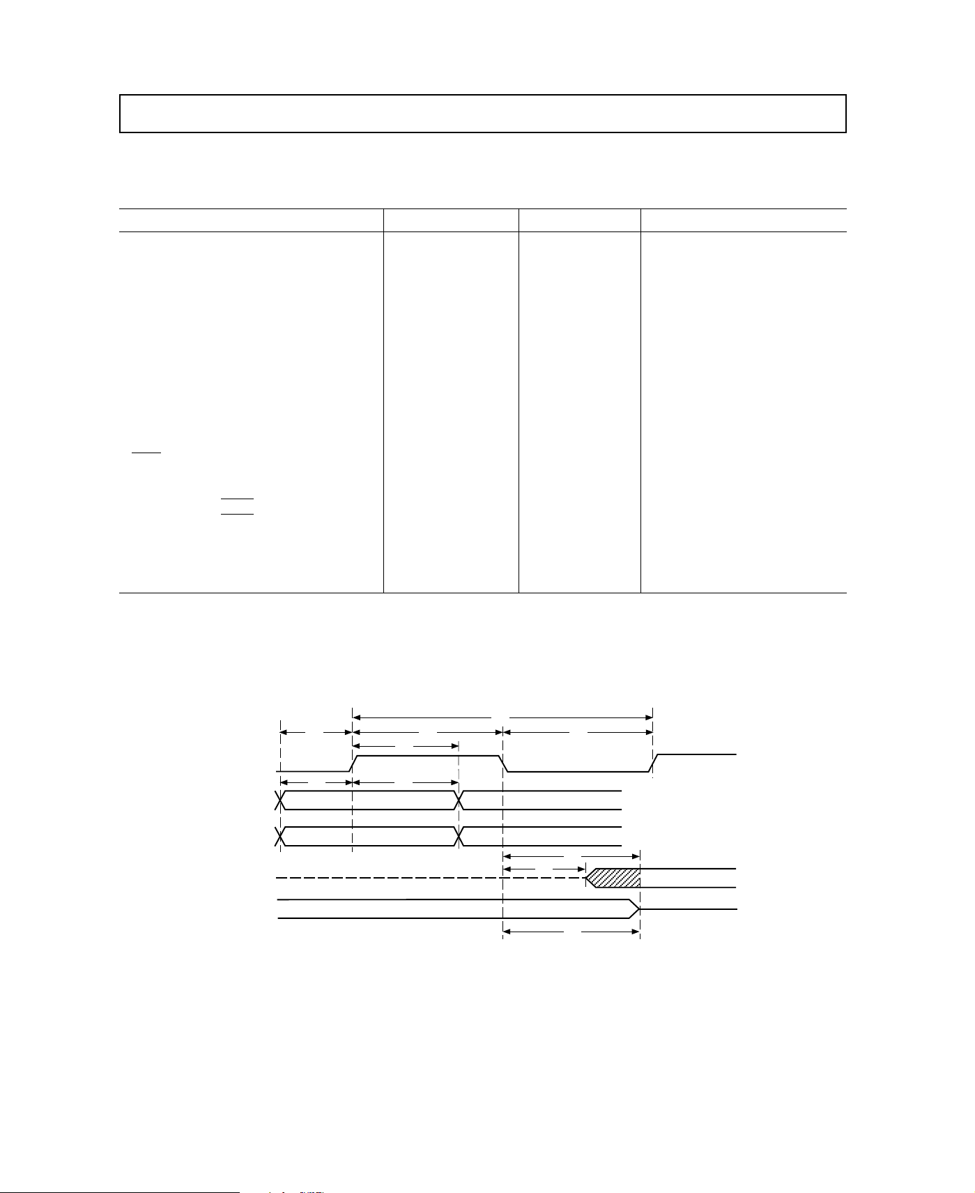
Figure 2. JTAG Timing
REV. 0
–5–
ADV7160/ADV7162
Timing Waveforms
CLOCK
CLOCK
LOADOUT
(2:1 MULTIPLEXING)
LOADOUT
(4:1 MULTIPLEXING)
LOADOUT
(8:1 MULTIPLEXING)
t
t
1
t
4
2
t
3
LOADIN
PIXEL INPUT
DATA
t
8
VALID
DATA
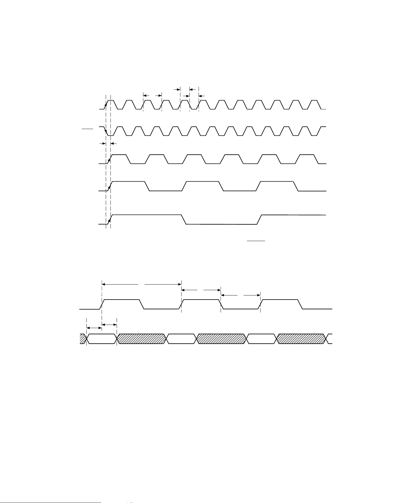
Figure 3. LOADOUT vs. Pixel Clock Input (CLOCK,
t
5
t
9
VALID
DATA
t
6
Figure 4. LOADIN vs. Pixel Input Data
t
7
CLOCK
VALID
DATA
)
–6–
REV. 0
CLOCK
LOADOUT
LOADIN
ADV7160/ADV7162
t
10
PIXEL
INPUT
DATA
ANALOG
OUTPUT
DATA
(IOR, IOG, IOB,
SYNCOUT
AN ...
H
N
DIGITAL INPUT TO ANALOG
OUTPUT PIPELINE
)
A
...
N+1
H
N+1
A
... H
N–1
N–1
t
PD
A
...
N+2
H
N+2
A
AN ... H
A
... H
N+1
N
N+1
N+2
... H
N+2
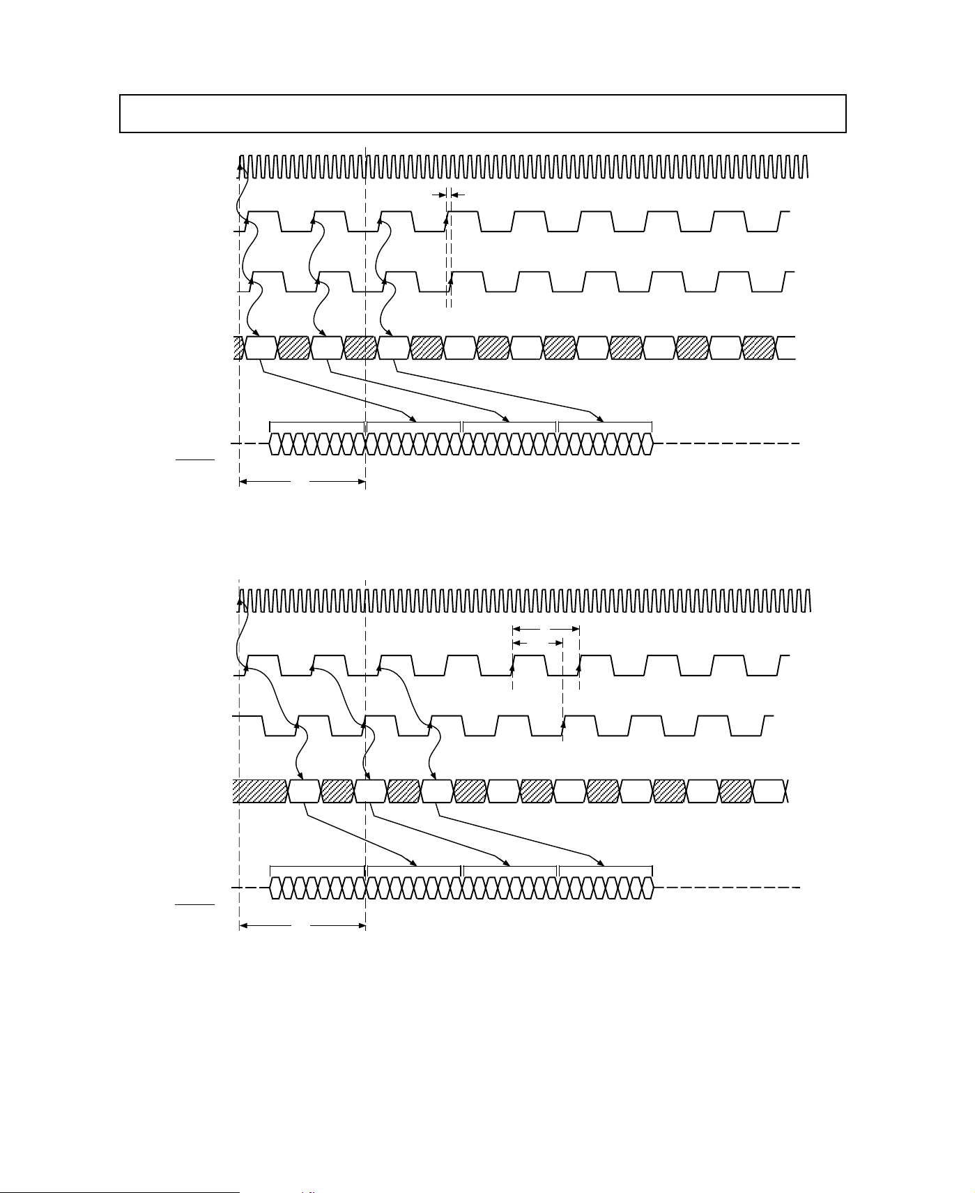
Figure 5. Pixel Input to Analog Output Pipeline with Minimum LOADOUT to LOADIN Delay (8:1 Multiplex Mode)
CLOCK
τ
τ-t
11
LOADOUT
LOADIN
PIXEL
INPUT
DATA
ANALOG
OUTPUT
DATA
(IOR, IOG, IOB,
SYNCOUT
)
AN ...
H
N
DIGITAL INPUT TO ANALOG
OUTPUT PIPELINE
A
... H
N–1
t
PD
N–1
A
N+1
H
N+1
...
AN ... H
A
...
N+2
H
N+2
A
A
... H
N+1
N
N+1
N+2
... H
N+2
Figure 6. Pixel Input to Analog Output Pipeline with Maximum LOADOUT to LOADIN Delay (8:1 Multiplex Mode)
REV. 0
–7–
ADV7160/ADV7162
CLOCK
LOADOUT
LOADIN
t
10
PIXEL
INPUT
DATA
ANALOG
OUTPUT
DATA
(IOR, IOG, IOB,
SYNCOUT
AN ...
D
N
)
A
...
N+1
D
N+1
DIGITAL INPUT TO ANALOG
OUTPUT PIPELINE
A
N–1
t
PD
A
N+2
D
... D
N+2
N–1
...
A
AN ... D
A
... D
N+1
N
N+1
N+2
... D
N+2
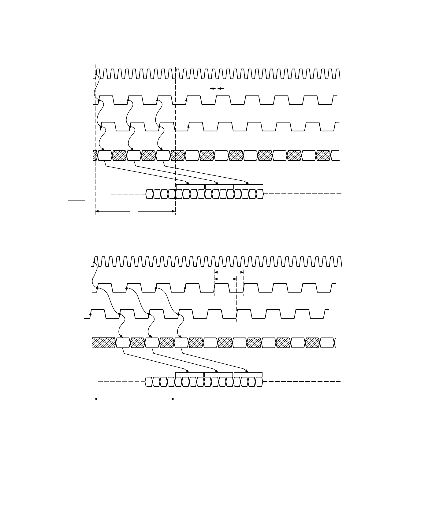
Figure 7. Pixel Input to Analog Output Pipeline with Minimum LOADOUT to LOADIN Delay (4:1 Multiplex Mode)
CLOCK
τ
τ-t
11
LOADOUT
LOADIN
PIXEL
INPUT
DATA
ANALOG
OUTPUT
DATA
(IOR, IOG, IOB,
SYNCOUT
)
AN ...
D
N
DIGITAL INPUT TO ANALOG
OUTPUT PIPELINE
A
...
N+1
D
N+1
A
N–1
t
PD
... D
N–1
A
N+2
D
N+2
...
AN ... D
A
A
... D
N+1
N
N+1
N+2
... D
N+2
Figure 8. Pixel Input to Analog Output Pipeline with Maximum LOADOUT to LOADIN Delay (4:1 Multiplex Mode)
–8–
REV. 0
CLOCK
LOADOUT
LOADIN
ADV7160/ADV7162
t
10
PIXEL
INPUT
DATA
ANALOG
OUTPUT
DATA
(IOR, IOG, IOB,
SYNCOUT
AN ...
B
N
)
A
...
N+1
B
N+1
DIGITAL INPUT TO ANALOG OUTPUT PIPELINE
A
...
N+2
B
N+2
t
PD
A
N–1BN–1AN
BNA
N+1BN+1AN+2
B
N+2
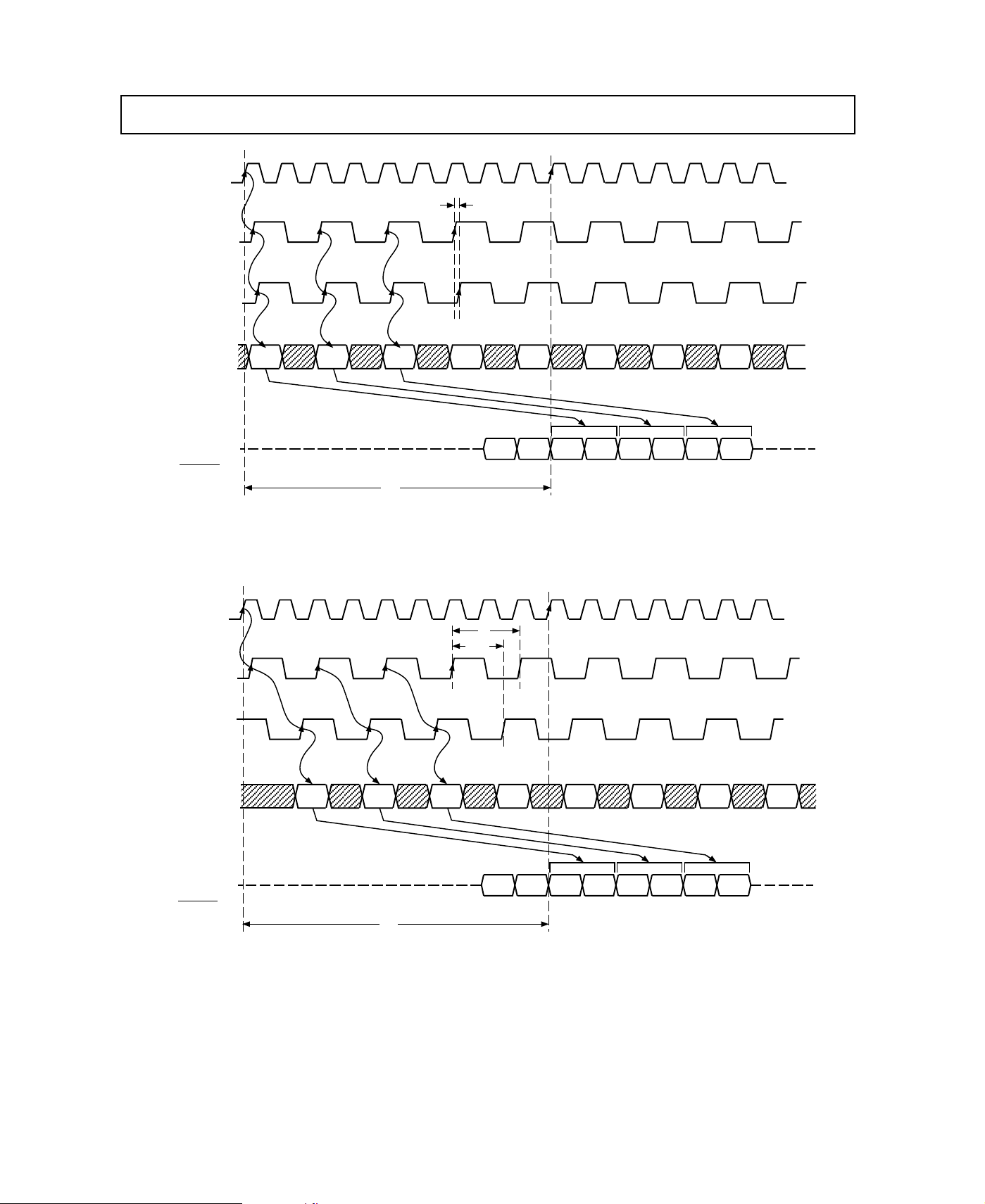
Figure 9. Pixel Input to Analog Output Pipeline with Minimum LOADOUT to LOADIN Delay (2:1 Multiplex Mode)
CLOCK
τ
τ-t
10
LOADOUT
LOADIN
PIXEL
INPUT
DATA
ANALOG
OUTPUT
DATA
(IOR, IOG, IOB,
SYNCOUT
)
AN ...
B
N
A
...
N+1
B
N+1
DIGITAL INPUT TO ANALOG OUTPUT PIPELINE
t
PD
A
B
N+2
N+2
...
A
N–1BN–1AN
A
B
N+1BN+1AN+2BN+2
N
Figure 10. Pixel Input to Analog Output Pipeline with Maximum LOADOUT to LOADIN Delay (2:1 Multiplex Mode)
REV. 0
–9–
ADV7160/ADV7162
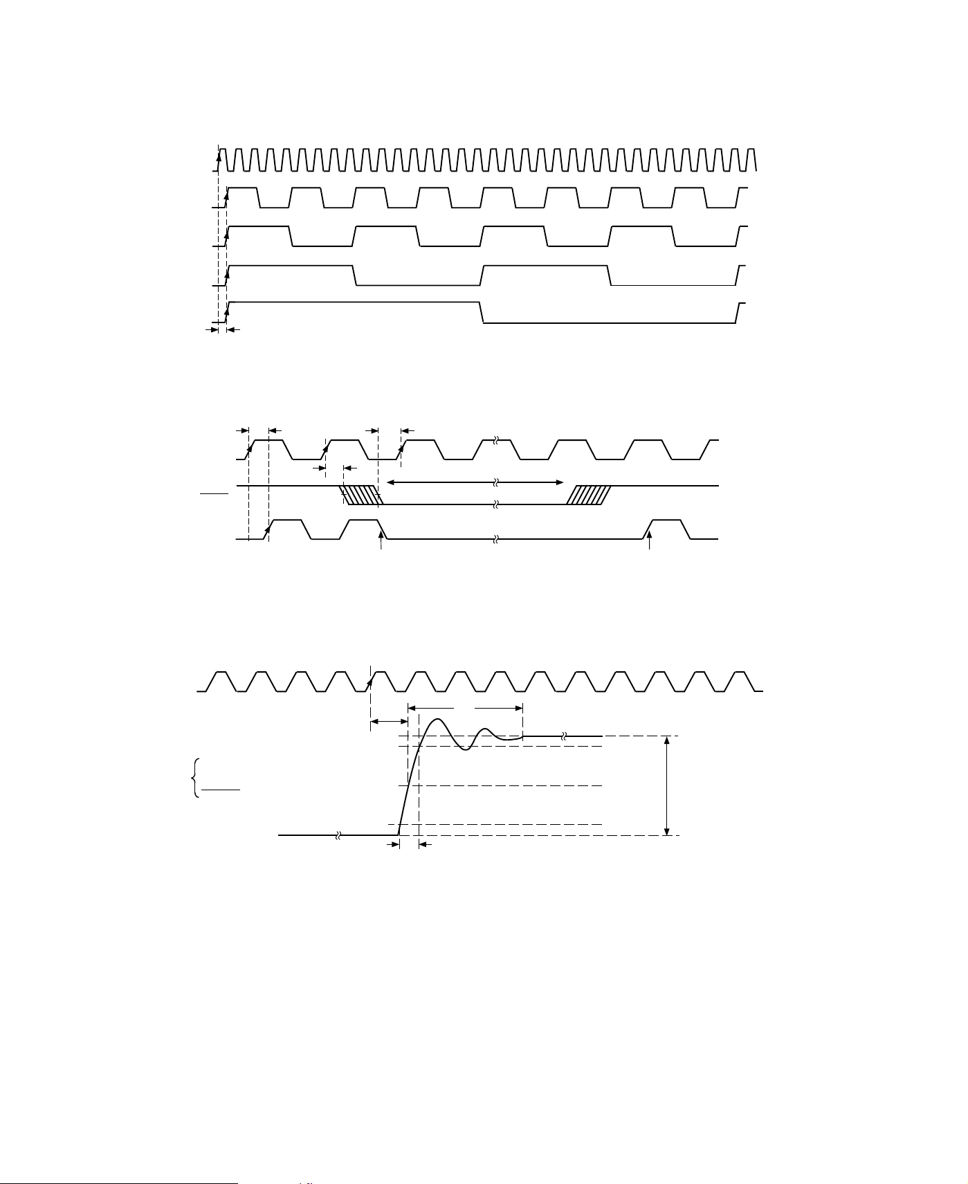
CLOCK
PRGCKOUT
(CLOCK/4)
PRGCKOUT
(CLOCK/8)
PRGCKOUT
(CLOCK/16)
PRGCKOUT
(CLOCK/32)
Figure 11. Pixel Clock Input vs. Programmable Clock Output (PRGCKOUT)
t
12
t
14
BLANKING PERIOD
START OF SCAN LINE (N+1)
SCKIN
BLANK
SCKOUT
t
13
t
15
END OF SCAN LINE (N)
Figure 12. Video Data Shift Clock Input (SCKIN) & BLANK vs. Video Data Shift Clock Output (SCKOUT)
CLOCK
t
18
WHITE LEVEL
90%
50%
10%
NOTE:
THIS DIAGRAM IS NOT TO SCALE. FOR THE PURPOSES OF CLARITY, THE
ANALOG OUTPUT WAVEFORM IS MAGNIFIED IN TIME AND AMPLLITUDE
W.R.T THE CLOCK WAVEFORM.
SYNCOUT IS A DIGITAL VIDEO OUTPUT SIGNAL.
IS THE ONLY RELEVANT TIMING SPECIFICATION FOR SYNCOUT.
t
16
FULL SCALE
TRANSITION
BLACK LEVEL
ANALOG
OUTPUTS
IOR
IOG
IOB
SYNCOUT
t
16
t
17
Figure 13. Analog Output Response vs. CLOCK
–10–
REV. 0
ADV7160/ADV7162
WARNING!
ESD SENSITIVE DEVICE
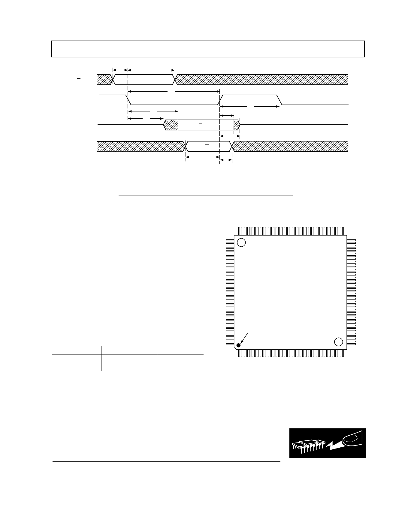
, C0, C1
R/W
CE
D0–D9
(READ MODE)
D0–D9
(WRITE MODE)
t
19
t
20
VALID
CONTROL DATA
t
24
t
23
t
21
R/W = 1
R/W
t
27
Figure 14. Microprocessor Port (MPU) Interface Timing
ABSOLUTE MAXIMUM RATINGS
1
VAA to GND . . . . . . . . . . . . . . . . . . . . . . . . . . . . . . . . . . . . 7 V
Voltage on Any Digital Pin . . . . . GND – 0.5 V to V
Ambient Operating Temperature (T
Storage Temperature (T
Junction Temperature (T
) . . . . . . . . . . . . . . . –65°C to +150°C
S
) . . . . . . . . . . . . . . . . . . . . . +150°C
J
) . . . . . . . . 0°C to +70°C
A
+ 0.5 V
AA
Lead Temperature (Soldering, 10 secs) . . . . . . . . . . . . +260°C
Vapor Phase Soldering (1 minute) . . . . . . . . . . . . . . . . +220°C
Analog Outputs to GND
NOTES
1
Stresses above those listed under “Absolute Maximum Ratings” may cause
permanent damage to the device. This is a stress rating only and functional
operation of the device at these or any other conditions above those listed in the
operational sections of this specification is not implied. Exposure to absolute
maximum rating conditions for extended periods may affect device reliability.
2
Analog Output Short Circuit to any Power Supply or Common can be of an
indefinite duration.
2
. . . . . . . . . . . . GND – 0.5 V to V
AA
= 0
121
t
t
25
t
26
t
28
22
160-Lead QFP Configuration
120 81
ROW C
ADV7160/ADV7162
QFP
ROW D
TOP VIEW
(NOT TO SCALE)
80
ROW B
ORDERING INFORMATION
Dot Clock Speed
1, 2, 3
160
PIN NO. 1
IDENTIFIER
220 MHz 170 MHz 140 MHz
3
ADV7160KS220
ADV7160KS1703ADV7160KS140
ADV7162KS2204ADV7162KS1704ADV7162KS140
NOTES
1
All devices are specified for 0°C to +70°C operation.
2
Contact Sales Office for latest information on package design.
3
ADV7160 is packaged in a 160-pin plastic power quad flatpack, QFP with
heatsink embedded.
4
ADV7162 is packaged in a standard 160-pin plastic quad flatpack, QFP.
3
4
1
CAUTION
ESD (electrostatic discharge) sensitive device. Electrostatic charges as high as 4000 V readily
accumulate on the human body and test equipment and can discharge without detection.
Although the ADV7160/ADV7162 features proprietary ESD protection circuitry, permanent
damage may occur on devices subjected to high energy electrostatic discharges. Therefore, proper
ESD precautions are recommended to avoid performance degradation or loss of functionality.
REV. 0
–11–
ROW A
41
40
ADV7160/ADV7162
ADV7160/ADV7162 PIN ASSIGNMENTS
Pin No. Mnemonic Pin No. Mnemonic Pin No. Mnemonic Pin No. Mnemonic
1G2
2G2
3G2
4G2
5G3
6G3
7G3
8G3
9G4
10 G4
11 G4
12 G4
13 G5
14 G5
15 G5
16 G5
17 G6
18 G6
19 G6
20 G6
21 G7
22 V
23 V
A
B
C
D
A
B
C
D
A
B
C
D
A
B
C
D
A
B
C
D
A
AA
AA
41 CLOCK 81 D9 121 R1
42 SCKIN 82 D8 122 R1
43 SCKOUT 83 D7 123 R2
44 V
45 PRGCKOUT 85 D5 125 R2
46 GND 86 D4 126 R2
47 LOADOUT 87 D3 127 R3
48 LOADIN 88 D2 128 R3
49 B0
50 B0
51 B0
52 B0
53 B1
54 B1
55 B1
56 B1
57 B2
58 B2
59 B2
60 B2
61 B3
62 B3
63 B3
24 GND 64 B3
25 GND 65 B4
26 V
AA
66 B4
27 GND 67 B4
28 PLL
29 G7
30 G7
31 G7
32 PS0
33 PS0
34 PS0
35 PS0
36 PS1
37 PS1
38 PS1
39 PS1
REF
B
C
D
A
B
C
D
A
B
C
D
68 B4
69 B5
70 B5
71 B5
72 B5
73 B6
74 B6
75 B6
76 B6
77 B7
78 B7
79 B7
40 CLOCK 80 B7
AA
C
D
84 D6 124 R2
A
B
C
D
A
B
C
D
A
B
C
D
A
B
C
D
A
B
C
D
A
B
C
D
A
B
C
D
A
B
C
D
89 D1 129 R3
90 D0 130 R3
91 C1 131 R4
92 C0 132 V
93 R/W 133 V
94 CE 134 GND
95 TCK 135 GND
96 TMS 136 R4
97 GND 137 R4
98 V
AA
138 R4
99 TDO 139 R5
100 TDI 140 R5
101 SYNCOUT 141 R5
102 TRISYNC 142 R5
103 ODD/EVEN 143 R6
104 SYNC 144 R6
105 BLANK 145 R6
106 V
REF
146 R6
107 IOB 147 R7
108 COMP 148 R7
109 R
110 V
111 V
SET
AA
AA
149 R7
150 GND
151 V
112 GND 152 R7
113 IOG 153 G0
114 IOR 154 G0
115 R0
116 R0
117 R0
118 R0
119 R1
120 R1
A
B
C
D
A
B
155 G0
156 G0
157 G1
158 G1
159 G1
160 G1
A
B
C
D
A
B
C
D
A
AA
AA
B
C
D
A
B
C
D
A
B
C
D
A
B
C
AA
D
A
B
C
D
A
B
C
D
–12–
REV. 0

Mnemonic Function
ADV7160/ADV7162
PIN FUNCTION DESCRIPTION
RED (R0
...R0B – R7A...R7D), GREEN (G0A...G0D – G7A...G7D), BLUE (B0A...B0D – B7A...B7D):
A
Pixel Port (TTL Compatible Inputs): 96 pixel select inputs, with 8 bits each for Red, Green and Blue.
Each bit is multiplexed [A-D] 4:1 or 2:1. It can be configured for 24-Bit True-Color Data, 8-Bit
Pseudo-Color Data, 16-Bit True-Color and 15-Bit True-Color Data formats. In 8-Bit Pseudo-Color
Mode, there is a special case whereby 8:1 multiplexing is also available. It will be explained in more
detail later. Pixel Data is latched into the device on the rising edge of LOADIN.
. . . PS0D, PS1A ...PS1
PS0
A
D
Palette Priority Selects (TTL Compatible Inputs): The eight PS inputs provide two Bits after input
multiplexing. These pixel port select inputs can be configured for three separate functions. In Overlay
Mode, these inputs provide a three color overlay function. With any value other than “00” on the
overlay inputs, the color displayed comes from the overlay palette instead of the main pixel inputs.
For the ADV7160, in Bypass Mode, PS1 specifies for each pixel whether it should pass through the
Color Matrix and Color Palette or bypass the Matrix and Palette. PS0 acts as an overlay input. (This
mode is not available for the ADV7162.) Palette Select Mode is used to multiplex the RGB outputs of
a number of devices. When the palette mode inputs match the PS bits in the mode register, the part
operates as normal. When there is a mismatch, the RGB outputs are switched to zero, allowing the
RGB outputs of another device to drive the monitor.
LOADIN Pixel Data Load Input (TTL Compatible Input): This input latches the multiplexed pixel data, in-
cluding PS0-PS1,
BLANK, TRISYNC, SYNC and ODD/EVEN into the device.
LOADOUT Pixel Data Load Output (TTL Compatible Output): This output control signal runs at a divided
down frequency of the pixel clock. Its frequency is a function of the multiplex rate. It can be used to
directly or indirectly drive LOADIN.
f
LOADOUT
= f
CLOCK
/M
where
(M = 2 for 2:1 Multiplex Mode)
(M = 4 for 4:1 Multiplex Mode)
(M = 8 for 8:1 Multiplex Mode)
PRGCKOUT Programmable Clock Output (TTL Compatible Output): This output control signal runs at a divided
down frequency of the pixel Clock. Its frequency is user programmable and is determined by bits
CR30 and CR31 of Command Register 3.
f
PRGCKOUT
= f
CLOCK
/N
where N = 4, 8, 16 & 32
SCKIN Video Shift Clock Input (TTL Compatible Input): The signal on this input is internally gated syn-
chronously with the
BLANK signal. The resultant output, SCKOUT, is a video clocking signal that
is stopped during video blanking periods. It is normally driven by a divided down version of the
CLOCK frequency.
SCKOUT Video Shift Clock Output (TTL Compatible Output): This output is a synchronously gated version of
SCKIN and
BLANK. SCKOUT is a video clocking signal that is stopped during video blanking
periods.
CLOCK,
CLOCK Clock Inputs (ECL Compatible Inputs): These differential clock inputs are designed to be driven by
ECL logic levels configured for single supply (+5 V) operation. The clock rate is normally the pixel
clock rate of the system.
PLL
REF
PLL Clock Input (TTL Compatible Input): This clock input is designed to be driven by TTL logic
levels. The PLL is then configured to output a specific frequency depending on the PLL Registers.
See PLL section for more detail.
BLANK Composite Blank (TTL Compatible Input): This video control signal drives the analog outputs to the
blanking level.
SYNC Composite-Sync Input (TTL Compatible Input): This video control signal drives any of the analog
outputs to the
Register 2 must be set if
Register 4 must be set if
Register 4 must be set if
SYNC level. It is only asserted during the blanking period. CR22 in Command
SYNC is to be decoded onto the IOG analog output, CR41 in Command
SYNC is to be decoded onto the IOR analog output, CR42 in Command
SYNC is to be decoded onto the IOB analog output, otherwise the SYNC
input is ignored.
REV. 0
–13–

ADV7160/ADV7162
Mnemonic Function
SYNCOUT Composite-Sync Output (TTL Compatible Output). This video output is a delayed version of
SYNC. The delay corresponds to the number of pipeline stages of the device.
TRISYNC Composite-Sync HDTV Control (TTL Compatible Output). This video input is enabled using Bit
CR17 in Command Register 1. When
goes to the tri-sync level. As with the
D9–D0 Data Bus (TTL Compatible Input/Output Bus). Data, including color palette values and device con-
trol information is written to and read from the device over this 10-bit, bidirectional databus. 10-bit
data or 8-bit data can be used. The databus can be configured for either 10-bit parallel data or byte
data (8+2) as well as standard 8-bit data. Any unused bits of the data bus should be terminated
through a resistor to either the digital power plane (V
ODD/
EVEN Odd/Even Control (TTL Compatible Input). This input indicates which field of the frame is being
displayed. It is required to ensure proper operation of the ADV7160/ADV7162 cursor when interlaced display mode is selected. It is ignored when noninterlaced display mode is selected. This input
should change only during the vertical blank period. It is assumed that an odd field will always follow
an even field and vice versa.
CE Chip Enable (TTL Compatible Input). This input must be at Logic “0” when writing to or reading
from the device over the data bus (D0–D9). Internally, data is latched on the rising edge of
R/
W Read/Write Control (TTL Compatible Input). This input determines whether data is written to or
read from the device’s registers and color palette RAM. R/
data to the part. R/
W must be at Logic “1” and CE at Logic “0” to read from the device.
C0, C1 Command Controls (TTL Compatible Inputs). These inputs determine the type of read or write op-
eration being performed on the device over the data bus, (see Interface Truth Table). Data on these
inputs is latched on the falling edge of
IOR, IOG, IOB Red, Green & Blue Current Outputs (High Impedance Current Sources). These RGB video outputs
are specified to directly drive RS-343A and RS-170 video levels into doubly terminated 75 Ω loads.
V
REF
Voltage Reference Input (Analog Input): An external 1.235 V voltage reference is required to drive
this input. An AD589 (2-terminal voltage reference) or equivalent is recommended. (Note: It is not
recommended to use a resistor network to generate the voltage reference.)
R
SET
Output Full Scale Adjust Control (Analog Input). A resistor connected between this pin and analog
ground controls the absolute amplitude of the output video signal. For a value of R
280 Ω, with 37.5 Ω termination and using CR43 and CR44 of Command Register 4 to set the DAC
Gain as shown, the required Video Standard can be achieved.
CR44 CR43 Video Standard DAC Gain Black to White
0 0 RS343A, Sync & Pedestal 3996 660 mV 17.62 mA
0 1 RS343A, Sync & No Pedestal 4224 699 mV 18.63 mA
1 0 RS343A, No Sync & No Pedestal 4311 714 mV 19.05 mA
1 1 RS170, Sync & Pedestal 5592 925 mV 24.67 mA
Alternatively, R
can be calculated by the following equation:
SET
COMP Compensation Pin. A 0.1 µF capacitor should be connected between this pin and V
V
AA
Power Supply (+5 V ± 5%). The part contains multiple power supply pins, all should be connected
together to one common +5 V filtered analog power supply.
GND: Analog Ground. The part contains multiple ground pins, all should be connected together to the
system’s ground plane.
TMS, TCK, These four pins control the JTAG test access port.
TDI, TDO See Appendix 6 for more detail
TRISYNC is low, any DAC output which has Sync enabled,
SYNC input, it should only be activated while BLANK is low.
) or GND.
CC
CE.
W and CE must be at Logic “0” to write
CE.
of nominally
SET
R
DAC Gain ×V
SET
Black to White Current
REF
AA
.
–14–
REV. 0
 Loading...