现货库存、技术资料、百科信息、热点资讯,精彩尽在鼎好!
CMOS 220 MHz True-Color Graphics
a
FEATURES
220 MHz, 24-Bit (30-Bit Gamma Corrected) True Color
Triple 10-Bit “Gamma Correcting” D/A Converters
Triple 256 3 10 (256 3 30) Color Palette RAM
On-Chip Clock Control Circuit
Palette Priority Select Registers
RS-343A/RS-170 Compatible Analog Outputs
TTL Compatible Digital Inputs
Standard MPU l/O Interface
10-Bit Parallel Structure
8+2 Byte Structure
Programmable Pixel Port: 24-Bit and 8-Bit (Pseudo)
Pixel Data Serializer
Multiplexed Pixel Input Ports; 1:1, 2:1
+5 V CMOS Monolithic Construction
100-Lead Plastic Quad Flatpack (QFP)
Thermally Enhanced to Achieve u
MODES OF OPERATION
24-Bit True Color (30-Bit Gamma Corrected)
@ 220 MHz
@ 170 MHz
@ 135 MHz
@ 110 MHz
@ 85 MHz
8-Bit Pseudo Color
15-Bit True Color
24
PALETTE
SELECTS
(PS0, PS1)
LOADIN
LOADOUT
SCKIN
SCKOUT
SYNC
BLANK
CLOCK
CLOCK
A
24
B
4
CLOCK CONTROL
SYNCHRONIZATION
÷32, ÷16, ÷8, ÷4, ÷2
ECL TO CMOS
RED (R0–R7),
GREEN (G0–G7),
BLUE (B0–B7)
COLOR DATA
PRGCKOUT
REV. B
Information furnished by Analog Devices is believed to be accurate and
reliable. However, no responsibility is assumed by Analog Devices for its
use, nor for any infringements of patents or other rights of third parties
which may result from its use. No license is granted by implication or
otherwise under any patent or patent rights of Analog Devices.
JC
V
AA
P
48
I
X
E
L
P
O
R
4
T
CLOCK DIVIDE
&
CIRCUIT
< 1.08C/W
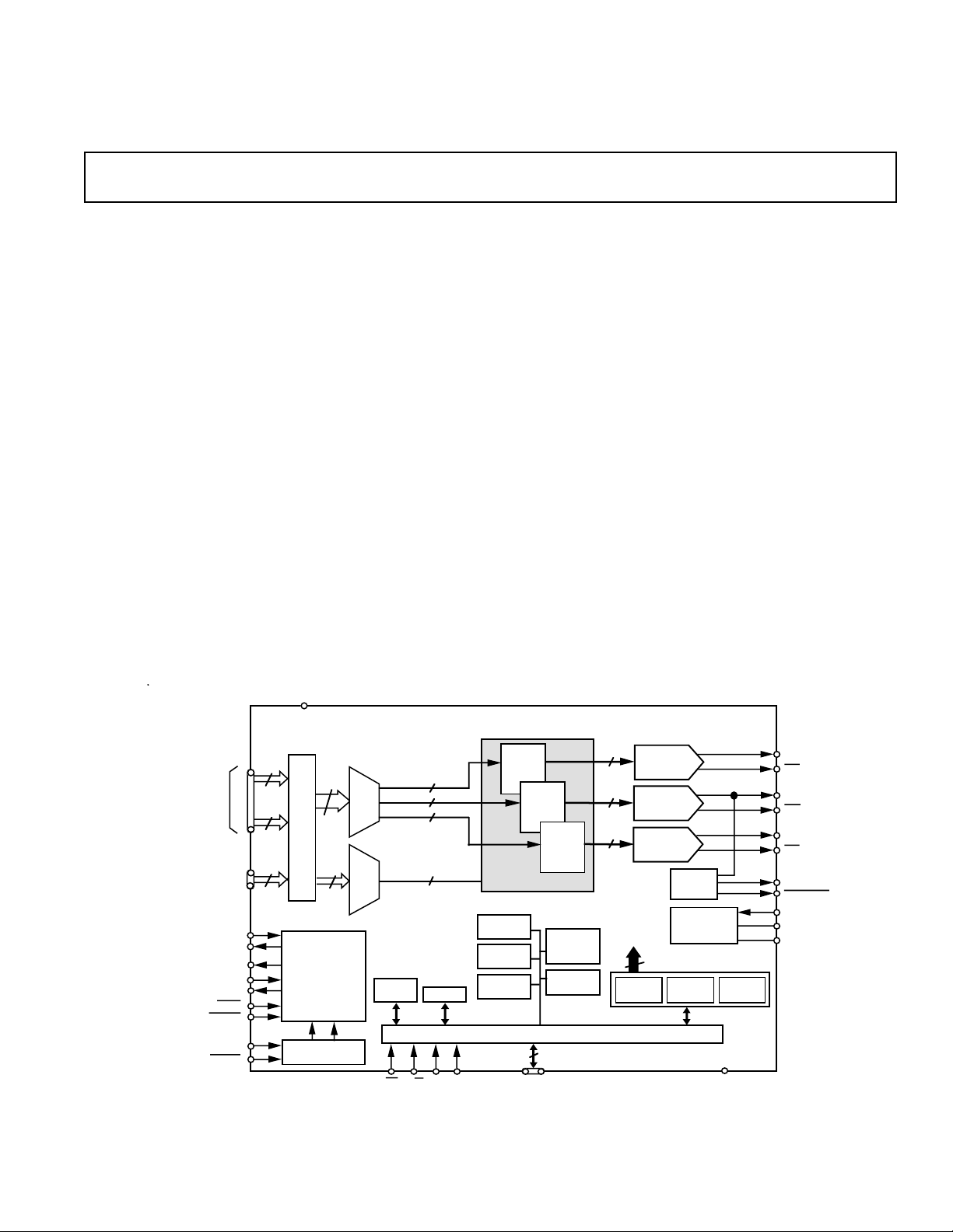
FUNCTIONAL BLOCK DIAGRAM
8
ADDRESS
ADDR
(A0-–A15)
CE
R/W
8
8
2
MODE
REGISTER
(MR1)
C0 C1
MUX
2:1
MUX
2:1
REGISTER
Triple 10-Bit Video RAM-DAC
ADV7152
APPLICATIONS
High Resolution, True Color Graphics
Professional Color Prepress Imaging
GENERAL DESCRIPTION
The ADV7152 (ADV®) is a complete analog output, Video
RAM-DAC on a single CMOS monolithic chip. The part is specifically designed for use in high performance, color graphics
workstations. The ADV7152 integrates a number of graphic
functions onto one device allowing 24-bit direct True-Color operation at the maximum screen update rate of 220 MHz. The
ADV7152 implements 30-bit True Color in 24-bit frame buffer
designs. The part also supports other modes, including 15-bit
True Color and 8-bit Pseudo or Indexed Color. Either the Red,
Green or Blue input pixel ports can be used for Pseudo Color.
The device consists of three, high speed, 10-bit, video D/A converters (RGB), three 256 3 10 (one 256 3 30) color look-up
tables, palette priority selects, a pixel input data multiplexer/
serializer and a clock generator/divider circuit. The ADV7152
implements 1:1 and 2:1 pixel data multiplexing. The onboard
palette priority select inputs enable multiple palette devices to
be connected together for use in multipalette and window
(Continued on page 10)
ADV is a registered trademark of Analog Devices, Inc.
256-COLOR/GAMMA
PALETTE RAM
RED
256 x 10
GREEN
256 x 10
BLUE
256 x 10
CONTROL REGISTERS
PIXEL MASK
REGISTER
TEST
REGISTERS
ID
REGISTER
REGISTERS
MPU PORT
10 (8+2)
D9 – D0
COMMAND
(CR1-CR3)
REGISTER
10 IOR
10
10
REVISION
RED DAC
GREEN DAC
BLUE DAC
DATA TO
PALETTES
30
RED
REGISTER
10-BIT
10-BIT
10-BIT
One Technology Way, P.O. Box 9106, Norwood, MA 02062-9106, U.S.A.
Tel: 617/329-4700 Fax: 617/326-8703
ADV7152
SYNC
OUTPUT
VOLTAGE
REFERENCE
CIRCUIT
COLOR REGISTERS
REGISTER
GND
BLUE
GREEN
REGISTER
IOR
IOG
IOG
IOB
IOB
I
PLL
SYNCOUT
V
REF
R
SET
C
OMP

ADV7152–SPECIFICATIONS
CL = 10 pF); IOR, IOG, IOB = GND. All specifications T
MIN
1
(V
= +5 V; V
AA
2
to T
unless otherwise noted.)
MAX
= +1.235 V; R
REF
= 280 V. IOR, IOG, IOB (RL = 37.5 V,
SET
Parameter All Versions Unit Test Conditions/Comments
STATIC PERFORMANCE
Resolution (Each DAC) 10 Bits
Accuracy (Each DAC)
Integral Nonlinearity ±1 LSB max
Differential Nonlinearity ±1 LSB max Guaranteed Monotonic
Gray Scale Error ±5 % Gray Scale max
Coding Binary
DIGITAL INPUTS (Excluding CLOCK, CLOCK)
Input High Voltage, V
Input Low Voltage, V
Input Current, I
Input Capacitance, C
INL
IN
IN
INH
2 V min
0.8 V max
±10 µA max VIN = 0.4 V or 2.4 V
10 pF typ
CLOCK INPUTS (CLOCK, CLOCK)
Input High Voltage, V
Input Low Voltage, V
Input Current, I
Input Capacitance, C
INL
IN
IN
INH
VAA – 1.0 V min
VAA – 1.6 V max
±10 µA max VIN = 0.4 V or 2.4 V
10 pF typ
DIGITAL OUTPUTS
Output High Voltage, V
Output Low Voltage, V
OL
OH
2.4 V min I
0.4 V max I
SOURCE
= 3.2 mA
SINK
= 400 µA
Floating-State Leakage Current 20 µA max
Floating-State Output Capacitance 20 pF typ
ANALOG OUTPUTS
Gray Scale Current Range 15/22 mA min/max
Output Current
White Level Relative to Blank 17.69/20.40 mA min/max Typically 19.05 mA
White Level Relative to Black 16.74/18.50 mA min/max Typically 17.62 mA
Black Level Relative to Blank 0.95/1.90 mA min/max Typically 1.44 mA
Blank Level on IOR, IOB 0/50 µA min Typically 5 µA
Blank Level on IOG 6.29/8.96 mA min/max Typically 7.62 mA
Sync Level on IOG 0/50 µA min/max Typically 5 µA
LSB Size 17.22 µA typ
DAC-to-DAC Matching 3 % max Typically 1%
Output Compliance, V
Output Impedance, R
OUT
Output Capacitance, C
OC
OUT
0/+1.4 V min/V max
100 kΩ typ
30 pF max I
OUT
= 0 mA
VOLTAGE REFERENCE
Voltage Reference Range, V
Input Current, I
VREF
REF
1.14/1.26 V min/V max V
+5 µA typ
= 1.235 V for Specified Performance
REF
POWER REQUIREMENTS
V
AA
3
I
AA
I
AA
I
AA
I
AA
I
AA
5 V nom
400 mA max 220 MHz Parts
370 mA max 170 MHz Parts
350 mA max 135 MHz Parts
330 mA max 110 MHz Parts
315 mA max 85 MHz Parts
Power Supply Rejection Ratio 0.5 %/% max Typically 0.12%/%, COMP = 0.1 µF
DYNAMIC PERFORMANCE
Clock and Data Feedthrough
Glitch Impulse 50 pV secs typ
DAC-to-DAC Crosstalk
NOTES
1
±5% for all versions.
2
Temperature range (T
3
Pixel Port is continuously clocked with data corresponding to a linear ramp. TJ = 100°C.
4
Clock and data feedthrough is a function of the amount of overshoot and undershoot on the digital inputs. Glitch impulse includes clock and data feedthrough.
5
TTL input values are 0 to 3 volts, with input rise/fall times ≤ 3 ns, measured the 10% and 90% points. Timing reference points at 50% for inputs and outputs.
6
DAC-to-DAC crosstalk is measured by holding one DAC high while the other two are making low-to-high and high-to-low transitions.
Specifications subject to change without notice.
MIN
to T
4, 5
6
): 0°C to +70°C; TJ (Silicon Junction Temperature) ≤ 100°C.
MAX
–30 dB typ
–23 dB typ
–2–
REV. B
ADV7152
1
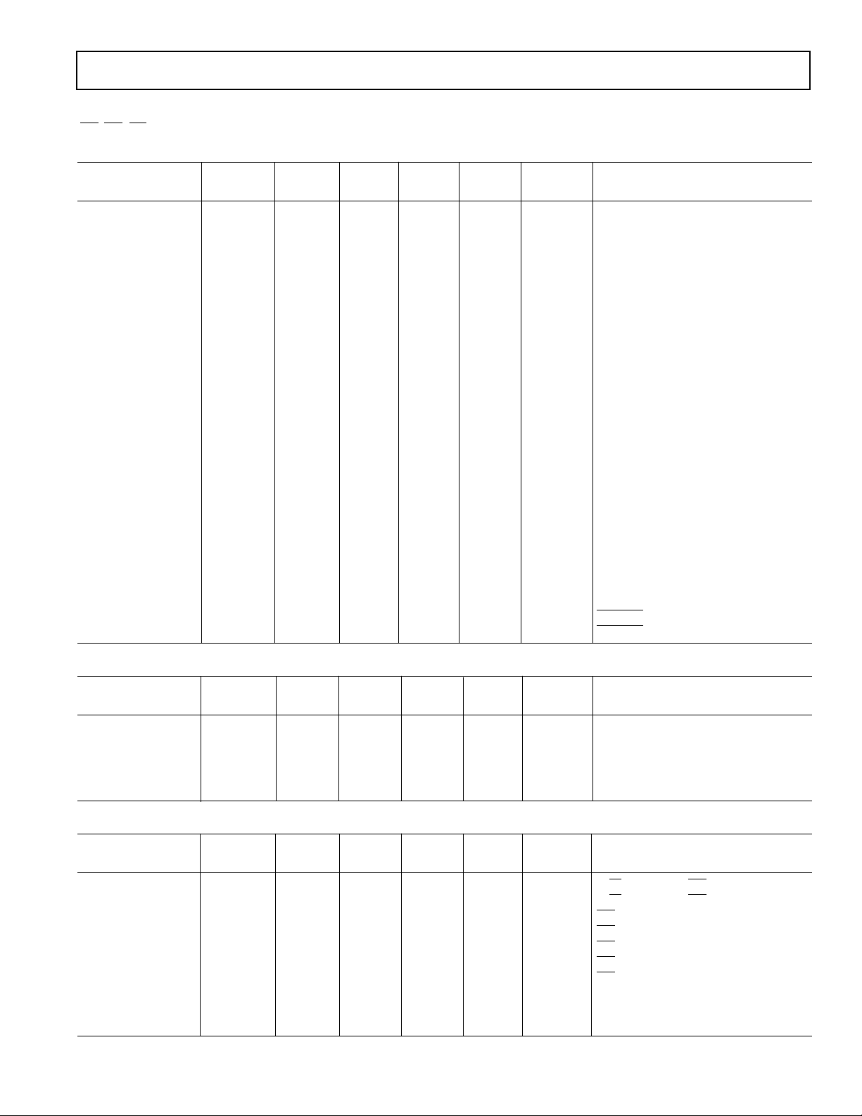
TIMING CHARACTERISTICS
IOR, IOG, I0B = GND. All specifications T
CLOCK CONTROL AND PIXEL PORT
220 MHz 170 MHz 135 MHz 110 MHz 85 MHz
Parameter Version Version Version Version Version Units Conditions/Comments
MIN
2
(V
= +5 V; V
AA
3
to T
unless otherwise noted.)
MAX
4
= +1.235 V; R
REF
= 280 V. IOR, IOG, IOB (RL = 37.5 V, CL = 10 pF);
SET
f
CLOCK
t
1
t
2
t
3
t
4
f
LOADIN
220 170 135 110 85 MHz max Pixel CLOCK Rate
4.55 5.88 7.4 9.1 11.77 ns min Pixel CLOCK Cycle Time
2 2.5 3 4 4 ns min Pixel CLOCK High Time
2 2.5 3.2 4 4 ns min Pixel CLOCK Low Time
10 10 10 10 10 ns max Pixel CLOCK to LOADOUT Delay
LOADIN Clocking Rate
1:1 Multiplexing 110 110 110 110 85 MHz max
2:1 Multiplexing 110 85 67.5 55 42.5 MHz max
t
5
LOADIN Cycle Time
1:1 Multiplexing 9.1 9.1 9.1 9.1 11.76 ns min
2:1 Multiplexing 9.1 11.76 14.8 18.18 23.53 ns min
t
6
LOADIN High Time
1:1 Multiplexing 44444ns min
2:1 Multiplexing 45689ns min
t
7
LOADIN Low Time
1:1 Multiplexing 44444ns min
2:1 Multiplexing 45689ns min
t
8
t
9
t
10
5
τ–t
11
6
t
PD
00000ns minPixel Data Setup Time
55555ns minPixel Data Hold Time
00000ns minLOADOUT to LOADIN Delay
τ–5 τ–5 τ–5 τ–5 τ–5 ns max LOADOUT to LOADIN Delay
Pipeline Delay
1:1 Multiplexing 55555CLOCKs (1 × CLOCK = t
2:1 Multiplexing 66666CLOCKs
t
12
t
13
t
14
t
15
10 10 10 10 10 ns max Pixel CLOCK to PRGCKOUT Delay
55555ns maxSCKIN to SCKOUT Delay
55555ns minBLANK to SCKIN Setup Time
11111ns minBLANK to SCKIN Hold Time
)
1
ANALOG OUTPUTS
7
220 MHz 170 MHz 135 MHz 110 MHz 85 MHz
Parameter Version Version Version Version Version Units Conditions/Comments
t
16
t
17
t
18
t
SK
15 15 15 15 15 ns typ Analog Output Delay
11111ns typAnalog Output Rise/Fall Time
15 15 15 15 15 ns typ Analog Output Transition Time
22222ns maxAnalog Output Skew (IOR, IOG, IOB)
00000ns typ
MPU PORTS
8, 9
220 MHz 170 MHz 135 MHz 110 MHz 85 MHz
Parameter Version Version Version Version Version Units Conditions/Comments
t
19
t
20
t
21
t
22
8
t
23
9
t
24
9
t
25
33333ns minR/W, C0, C1 to CE Setup Time
10 10 10 10 10 ns min R/W, C0, C1 to CE Hold Time
45 45 45 45 45 ns min CE Low Time
25 25 25 25 25 ns min CE High Time
55555ns minCE Asserted to Databus Driven
45 45 45 45 45 ns max CE Asserted to Data Valid
20 20 20 20 20 ns max CE Disabled to Databus Three-Stated
55555ns min
t
26
t
27
20 20 20 20 20 ns min Write Data (D0–D9) Setup Time
55555ns minWrite Data (D0–D9) Hold Time
REV. B
–3–
ADV7152
NOTES
1
TTL input values are 0 to 3 volts, with input rise/fall times ≤ 3 ns, measured between the 10% and 90% points. ECL inputs (CLOCK, CLOCK) are
VAA–0.8 V to VAA–1.8 V, with input rise/fall times ≤ 2 ns, measured between the 10% and 90% points. Timing reference points at 50% for inputs and outputs. Analog output load ≤ 10 pF. Databus (D0–D9) loaded as shown in Figure 1. Digital output load for LOADOUT, PRGCKOUT, SCKOUT, I
SYNCOUT ≤ 30 pF.
2
±5% for all versions.
3
Temperature range (T
4
Pixel Port consists of the following inputs: Pixel Inputs: RED [A, B]; GREEN [A, B]; BLUE [A, B], Palette Selects: PS0 [A, B]; PS1 [A, B]; Pixel Controls:
SYNC, BLANK; Clock Inputs: CLOCK, CLOCK, LOADIN, SCKIN; Clock Outputs: LOADOUT, PRGCKOUT, SCKOUT.
5
τ is the LOADOUT Cycle Time and is a function of the Pixel CLOCK Rate and the Multiplexing Mode: 1:1 multiplexing; τ = CLOCK = t1 ns; 2:1 multi-
plexing, τ = CLOCK × 2 = 2 × t1 ns.
6
These fixed values for Pipeline Delay are valid under conditions where t10 and τ–t11 are met. If either t10 or τ–t11 are not met, the part will operate but the Pipe-
line Delay is increased by 2 clock cycles for 2:1 mode after calibration cycle is performed.
7
Output delay measured from the 50% point of the rising edge of CLOCK to the 50% point of full-scale transition. Output rise/fall time measured between the
MIN
to T
): 0°C to +70°C; TJ (Silicon Junction Temperature) ≤ 100°C.
MAX
10% and 90% points of full-scale transition. Settling time measured from the 50% point of full-scale transition to the output remaining within ±1 LSB. (Settling time
does not include clock and data feedthrough.)
8
t23 and t24 are measured with the load circuit of Figure 1 and defined as the time required for an output to cross 0.4 V or 2.4 V.
9
t25 is derived from the measured time taken by the data outputs to change by 0.5 V when loaded with the circuit of Figure 1. The measured number is then extrapo-
lated back to remove the effects of charging the 100 pF capacitor. This means that the time, t25, quoted in the Timing Characteristics is the true value for the device
and as such is independent of external databus loading capacitances.
Specifications subject to change without notice.
I
SINK
PLL
and
CLOCK
CLOCK
LOADOUT
(1:1 MULTIPLEXING)
LOADOUT
(2:1 MULTIPLEXING)
LOADIN
PIXEL INPUT
DATA*
TO
OUTPUT
PIN
100pF
I
SOURCE
+2.1V
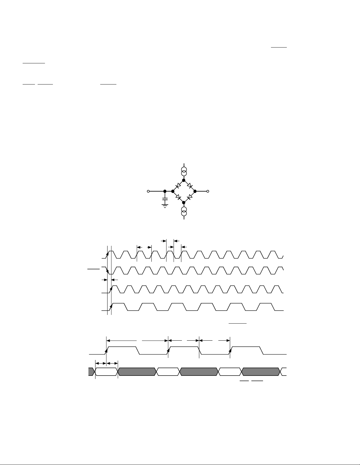
Figure 1. Load Circuit for Databus Access and Relinquish Times
t
2
VALID
DATA
t
3
t
t
6
CLOCK
7
VALID
DATA
)
t
1
t
4
Figure 2. LOADOUT vs. Pixel Clock Input (CLOCK,
t
5
t8t
9
VALID
DATA
*INCLUDES PIXEL DATA (R0-R7, G0-G7, B0-B7); PALETTE SELECT INPUTS (PS0-PS1); SYNC; BLANK
Figure 3. LOADIN vs. Pixel Input Data
–4–
REV. B
CLOCK
LOADOUT
LOADIN
ADV7152
t
10
PIXEL INPUT
DATA*
ANALOG
OUTPUT
DATA
A
N
B
N
IOR, IOR
IOG, IOG
IOB, IOB
I
A
N+1BN+1
DIGITAL INPUT TO ANALOG OUTPUT PIPELINE
, SYNCOUT
PLL
t
PD
A
N+2BN+2
A
N-1BN-1
A
N
A
B
N+1
N
A
B
N+2BN+2
N+1
*INCLUDES PIXEL DATA (R0–R7, G0–G7, B0–B7); PALETTE SELECT INPUTS (PS0-PS1); SYNC; BLANK
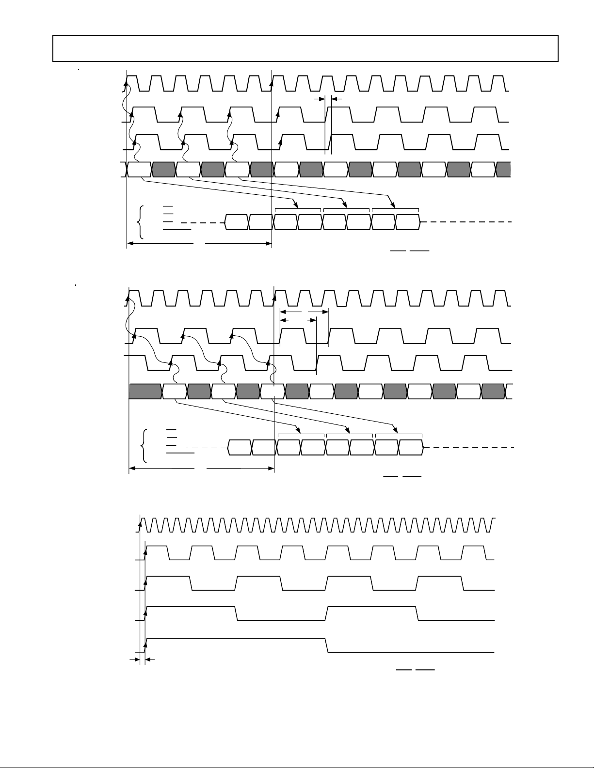
Figure 4. Pixel Input to Analog Output Pipeline with Minimum LOADOUT to LOADIN Delay (2:1 Multiplex Mode)
CLOCK
τ
τ- t
11
LOADOUT
LOADIN
PIXEL INPUT
DATA*
ANALOG
OUTPUT
DATA
*INCLUDES PIXEL DATA (R0–R7, G0–G7, B0–B7); PALETTE SELECT INPUTS (PS0–PS1); SYNC; BLANK
A
B
N
N
DIGITAL INPUT TO ANALOG OUTPUT PIPELINE
A
N+1BN+1
IOR, IOR
IOG, IOG
IOB, IOB
I
, SYNCOUT
PLL
t
PD
A
N-1BN-1
A
N+2BN+2
B
A
BNA
N
N+1
N+1
A
N+2BN+2
Figure 5. Pixel Input to Analog Output Pipeline with Maximum LOADOUT to LOADIN Delay (2:1 Multiplex Mode)
CLOCK
PRGCKOUT
(CLOCK/4)
PRGCKOUT
(CLOCK/8)
PRGCKOUT
(CLOCK/16)
PRGCKOUT
(CLOCK/32)
t
12
*INLCUDES PIXEL DATA (R0-R7, G0-G7, B0-B7); PALETTE SELECT INPUTS (PS0-PS1); SYNC; BLANK
Figure 6. Pixel Clock Input vs. Programmable Clock Output (PRGCKOUT)
REV. B
–5–
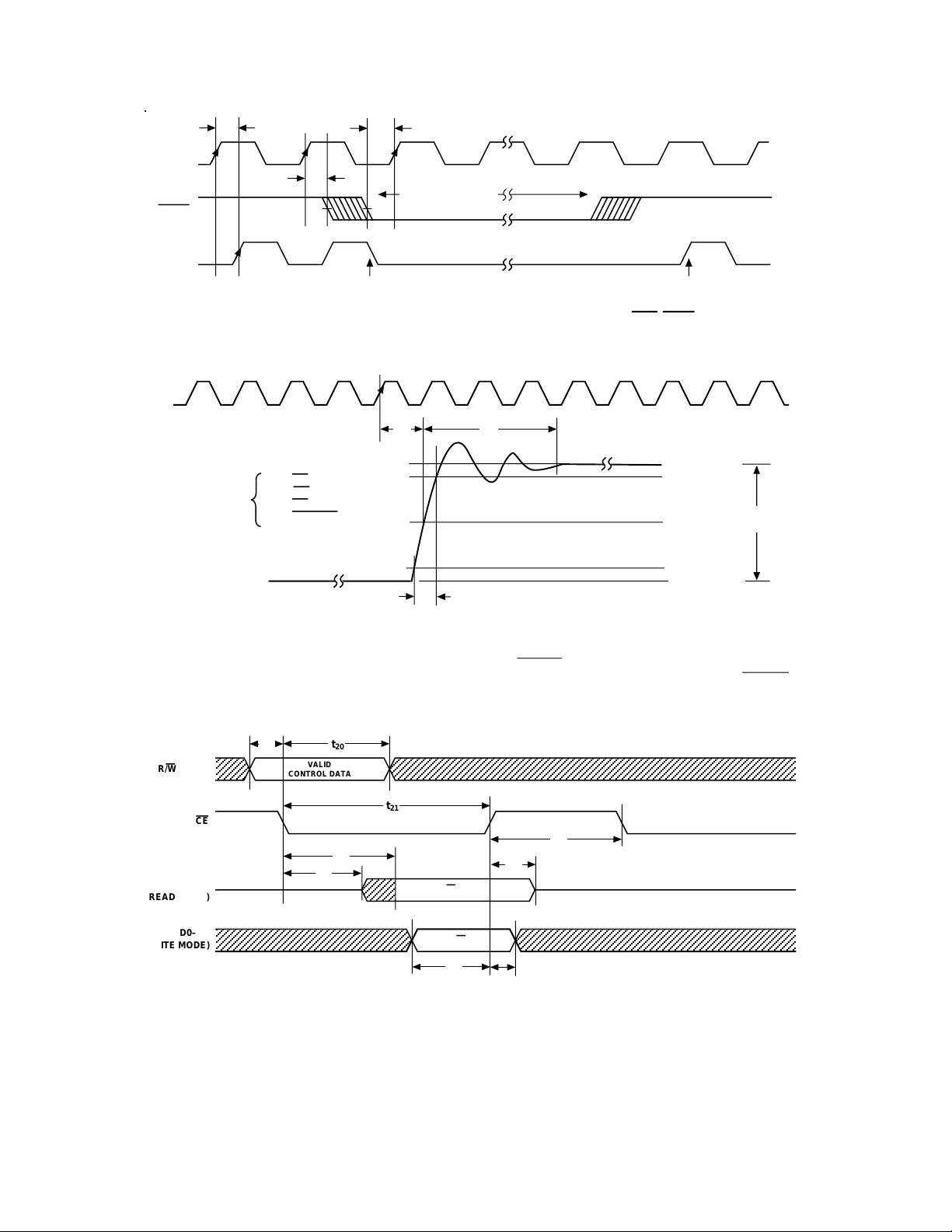
ADV7152
t
14
END OF SCAN
LINE (N)
BLANKING PERIOD
START OF SCAN
LINE (N+1)
SCKIN
BLANK
SCKOUT
t
13
t
15
*INCLUDES PIXEL DATA (R0-R7, G0-G7, B0-B7); PALETTE SELECT INPUTS (PS0-PS1); SYNC; BLANK
Figure 7. Video Data Shift Clock Input (SCKIN) & BLANK vs. Video Data Shift Clock Output (SCKOUT)
CLOCK
t
18
WHITE LEVEL
90 %
50 %
10 %
BLACK LEVEL
NOTE:
THIS DIAGRAM IS NOT TO SCALE. FOR THE PURPOSES OF CLARITY,
THE ANALOG OUTPUT WAVEFORM IS MAGNIFIED IN TIME AND
AMPLITUDE W.R.T. THE CLOCK WAVEFORM.
AND SYNCOUT ARE DIGITAL OUTPUT SIGNALS. t16 IS THE ONLY
I
PLL
RELEVANT OUTPUT TIMING SPECIFICATION FOR I
FULL SCALE
TRANSITION
AND SYNCOUT.
PLL
ANALOG
OUTPUTS
IOR, IOR
IOG, IOG
IOB, IOB
I
, SYNCOUT
PLL
t
16
t
17
R/W, C0, C1
CE
D0–D9
(READ MODE)
D0–D9
(WRITE MODE)
Figure 8. Analog Output Response vs. CLOCK
t
19
t
20
VALID
CONTROL DATA
t
t
23
t
21
t
22
24
R/W = 1
R/W = 0
t
26
t
25
t
27
Figure 9. Microprocessor Port (MPU) Interface Timing
–6–
REV. B
ADV7152
WARNING!
ESD SENSITIVE DEVICE
RECOMMENDED OPERATING CONDITIONS
Parameter Symbol Min Typ Max Units
Power Supply V
Ambient Operating Temperature T
Reference Voltage V
Output Load R
CAUTION
ESD (electrostatic discharge) sensitive device. Electrostatic charges as high as 4000 V readily
accumulate on the human body and test equipment and can discharge without detection.
Although the ADV7152 features proprietary ESD protection circuitry, permanent damage may
occur on devices subjected to high energy electrostatic discharges. Therefore, proper ESD
precautions are recommended to avoid performance degradation or loss of functionality.
ABSOLUTE MAXIMUM RATINGS
VAA to GND . . . . . . . . . . . . . . . . . . . . . . . . . . . . . . . . . . . 7 V
Voltage on Any Digital Pin . . . . GND – 0.5 V to V
Ambient Operating Temperature (T
Storage Temperature (T
Junction Temperature (T
Lead Temperature (Soldering, 10 secs) . . . . . . . . . . . +260°C
Vapor Phase Soldering (1 minute) . . . . . . . . . . . . . . . +220°C
Analog Outputs to GND
NOTES
1
Stresses above those listed under “Absolute Maximum Ratings” may cause
permanent damage to the device. This is a stress rating only and functional
operation of the device at these or any other conditions above those listed in the
operational sections of this specification is not implied. Exposure to absolute
maximum rating conditions for extended periods may affect device reliability.
2
Analog Output Short Circuit to any Power Supply or Common can be of an
indefinite duration.
220 MHz ADV7152LS220 110 MHz ADV7152LS110
170 MHz ADV7152LS170 85 MHz ADV7152LS85
135 MHz ADV7152LS135
NOTES
1
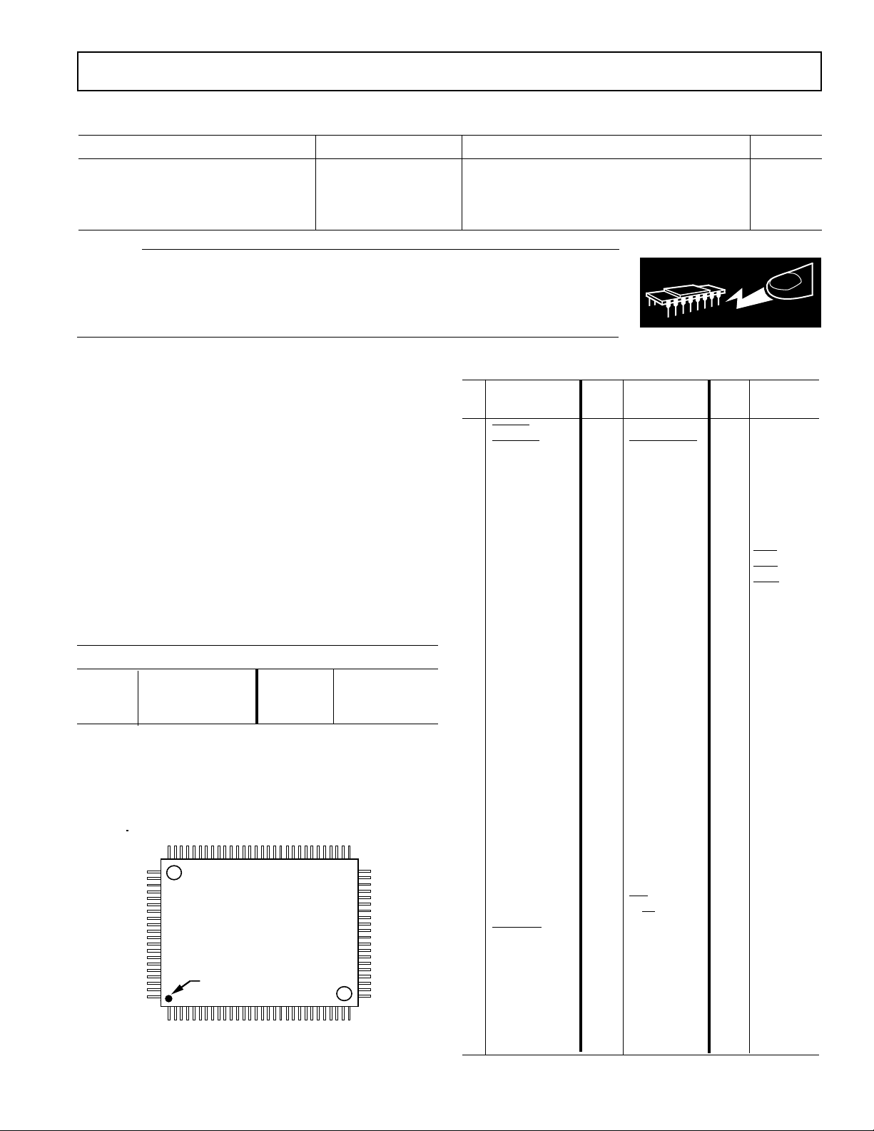
ADV7152 is packaged in a 100-pin plastic quad flatpack, QFP.
2
All devices are specified for 0°C to +70°C operation.
3
Contact sales office for latest information on package design.
REV. B
100
) . . . . . . . . . . . . . . –65°C to +150°C
S
) . . . . . . . . . . . . . . . . . . . . +150°C
J
2
. . . . . . . . . . . . . GND – 0.5 to V
ORDERING GUIDE
Speed
100-Lead QFP Configuration
80
81
ROW D
PIN NO. 1 IDENTIFIER
1
ROW C
ADV7152
QFP
Top View
(Not to Scale)
ROW A
AA
A
REF
L
1
+ 0.5 V
) . . . . . –55°C to +125°C
A
1, 2, 3
AA
51
50
ROW B
31
30
4.75 5.00 5.25 Volts
0 +70 °C
1.14 1.235 1.26 Volts
37.5 Ω
PIN ASSIGNMENTS
Pin Pin Pin
No. Mnemonic No. Mnemonic No. Mnemonic
1 SYNC 41 SCKOUT 81 D5
2
BLANK 42 SYNCOUT 82 V
3R0
4R0
AA
5 GND 45 GND 85 D8
6R1
7R1
8R2
9R2
10 R3
11 R3
12 R4
13 R4
14 R5
15 R5
16 R6
17 R6
18 R7
19 R7
20 G0
21 G0
22 G1
23 G1
24 G2
25 G2
A
B
A
B
A
B
A
B
A
B
A
B
A
B
A
B
A
B
A
B
A
B
26 NC 66 B5
27 G3
28 G3
29 G4
30 G4
31 G5
32 G5
33
A
B
A
B
A
B
CLOCK 73 C0
43 GND 83 D6
44 GND 84 D7
46 GND 86 D9
47 G6
48 G6
49 G7
50 G7
51 PS0
52 PS0
53 PS1
54 PS1
55 B0
56 B0
57 B1
5 8 B1
5 9 B2
60 B2
61 B3
62 B3
63 B4
64 B4
65 B5
67 B6
68 B6
69 B7
70 B7
A
B
A
B
A
B
A
B
A
B
A
B
A
B
A
B
A
B
A
B
A
B
A
B
87 GND
88 GND
89 IOB
90 IOR
91 IOG
92 IOB
93 IOG
94 V
95 I
96 IOR
97 COMP
98 V
99 R
100 V
71 CE
72 R/W
34 CLOCK 74 C1
35 LOADIN 75 D0
36 LOADOUT 76 D1
37 V
38 V
AA
AA
77 D2
78 GND
39 PRGCKOUT 79 D3
40 SCKIN 80 D4
NC = NO CONNECT.
–7–
AA
AA
PLL
REF
SET
AA
ADV7152
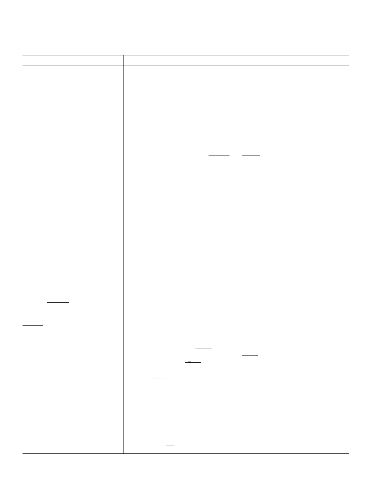
PIN FUNCTION DESCRIPTION
Mnemonic Function
RED (R0A . . . R0B–R7A . . . R7B), Pixel Port (TTL Compatible Inputs). 48 pixel select inputs, with 8 bits each for Red, 8
GREEN (G0
BLUE (B0
PS0
. . . PS0B, PS1A . . . PS1
A
LOADIN Pixel Data Load Input (TTL Compatible Input). This input latches the multiplexed
LOADOUT Pixel Data Load Output (TTL Compatible Output). This output control signal runs at a
PRGCKOUT Programmable Clock Output (TTL Compatible Output). This output control signal
SCKIN Video Shift Clock Input (TTL Compatible Input). The signal on this input is internally
SCKOUT Video Shift Clock Output (TTL Compatible Output). This output is a synchronously
CLOCK,
BLANK Composite Blank (TTL Compatible Input). This video control signal drives the analog
SYNC Composite-Sync Input (TTL Compatible Input). This video control signal drives the
SYNCOUT Composite SYNC O/P (TTL Compatible Output). This video output is a delayed ver-
D0–D9 Databus (TTL Compatible Input/Output Bus). Data, including color palette values and
CE Chip Enable (TTL Compatible Input). This input must be at Logic “0” when writing to
. . . G0B–G7A. . . G7B), bits for Green and 8 bits for Blue. Each bit is multiplexed [A-B] 2:1 or 1:1. It can be
A
. . . B0B–B7A . . . B7B) c onfigured for 24-Bit True-Color Data, 8-Bit Pseudo-Color Data and 15-Bit True-Color
A
Data formats. Pixel Data is latched into the device on the rising edge of LOADIN.
B
Palette Priority Selects (TTL Compatible Inputs): These pixel port select inputs determine whether or not the device’s pixel data port is selected on a pixel by pixel basis. The
palette selects allow switching between multiple palette devices. The device can be preprogrammed to completely shut off the DAC analog outputs. If the values of PS0 and
PS1 match the values programmed into bits MR16 and MR17 of the Mode Register,
then the device is selected. Each bit is multiplexed [A-B] 2:1 or 1:1. PS0 and PS1 are
latched into the device on the rising edge of LOADIN.
pixel data, including PS0–PS1,
BLANK and SYNC into the device.
divided down frequency of the pixel CLOCK input. Its frequency is a function of the
multiplex rate. It can be used to directly or indirectly drive LOADIN
f
LOADOUT
= f
CLOCK
/M
where (M = 1 for 1:1 Multiplex Mode)
where (M = 2 for 2:1 Multiplex Mode).
runs at a divided down frequency of the pixel CLOCK input. Its frequency is user
programmable and is determined by bits CR30 and CR31 of Command Register 3
f
PRGCKOUT
= f
CLOCK
/N
where N = 4, 8, 16 and 32.
gated synchronously with the
BLANK signal. The resultant output, SCKOUT, is a
video clocking signal that is stopped during video blanking periods.
gated version of SCKIN and
BLANK. SCKOUT, is a video clocking signal that is
stopped during video blanking periods.
CLOCK Clock Inputs (ECL Compatible Inputs). These differential clock inputs are designed to
be driven by ECL logic levels configured for single supply (+5 V) operation. The clock
rate is normally the pixel clock rate of the system.
outputs to the blanking level.
IOG analog output to the
CR22 in Command Re
output, otherwise the
sion of
SYNC. The delay corresponds to the number of pipeline stages of the device.
SYNC level. It is only asserted during the blanking period.
gister 2 must be set if SYNC is to be decoded onto the analog
SYNC input is ignored.
device control information is written to and read from the device over this 10-bit, bidirectional databus. 10-bit data or 8-bit data can be used. The databus can be configured
for either 10-bit parallel data or byte data (8+2) as well as standard 8-bit data. Any unused bits of the databus should be terminated through a resistor to either he digital
power plane (V
) or GND.
CC
or reading from the device over the databus (D0–D9). Internally, data is latched on the
rising edge of CE.
–8–
REV. B

ADV7152
Mnemonic Function
R/
W Read/Write Control (TTL Compatible Input). This input determines whether data is
written to or read from the device’s registers and color palette RAM. R/
be at Logic “0” to write data to the part. R/
W must be at Logic “1” and CE at Logic
“0” to read from the device.
C0, C1 Command Controls (TTL Compatible Inputs). These inputs determine the type of read
or write operation being performed on the device over the databus (see Interface Truth
Table). Data on these inputs is latched on the falling edge of
IOR, IOG; IOG, IOB; Red, Green and Blue Current Outputs (High Impedance Current Sources). These RGB
IOR;
CE.
IOB video outputs are specified to directly drive RS-343A and RS-170 video levels into dou-
bly terminated 75 Ω loads.
IOR, IOG and IOB are the complementary outputs of IOR, IOG and IOB. These out-
puts can be tied to GND if it is not required to use differential outputs.
V
REF
Voltage Reference Input (Analog Input). An external 1.235 V voltage reference is required to drive this input. An AD589 (2-terminal voltage reference) or equivalent is recommended. (Note: It is not recommended to use a resistor network to generate the
voltage reference.)
R
SET
Output Full-Scale Adjust Control (Analog Input). A resistor connected between this pin
and analog ground controls the absolute amplitude of the output video signal. The value
of R
is derived from the full-scale output current on IOG according to the following
SET
equations:
R
(Ω) = C1 × R
SET
R
(Ω) = C2 × R
SET
/IOG (mA); SYNC on GREEN
REF
/IOG (mA); No SYNC on GREEN.
REF
Full-Scale output currents on IOR and IOB for a particular value of R
IOR (mA)= C2 × R
REF
(V)/R
SET
(Ω)
and
IOB (mA) = C2 × R
REF
(V)/R
SET
(Ω)
where C1 = 6,050: PEDESTAL = 7.5 IRE
where C1 = 5,723: PEDESTAL = 0 IRE
and
where C2 = 4,323: PEDESTAL = 7.5 IRE
where C1 = 3,996: PEDESTAL = 0 IRE.
COMP Compensation Pin. A 0.1 µF capacitor should be connected between this pin and VAA.
I
PLL
Phase Lock Loop Output Current (High Impedance Current Source). This output is
used to enable multiple ADV7150/ADV7152s along with ADV7151s to be synchronized
together with subpixel resolution when using an external PLL. This output is triggered
either from the falling edge of
SYNC or BLANK as determined by bit CR21 of Com-
mand Register 2. When activated, it supplies a current corresponding to
I
(mA) = 1,728 × R
PLL
When not using the I
V
AA
Power Supply (+5 V ± 5%). The part contains multiple power supply pins, all should be
function, this output pin should be tied to GND.
PLL
REF
(V)/R
SET
(Ω)
connected together to one common +5 V filtered analog power supply.
GND Analog Ground. The part contains multiple ground pins, all should be connected
together to the system’s ground plane.
W and CE must
are given by:
SET
REV. B
–9–
ADV7152
(Continued from page 1)
applications. The part is controlled and programmed through
the microprocessor (MPU) port. The part also contains a number of onboard test registers, associated with self diagnostic testing of the device.
The individual Red, Green and Blue pixel input ports allow
True-Color, image rendition. True-Color image rendition, at
speeds of up to 220 MHz, is achieved through the use of the
onboard data multiplexer/serializer. The pixel input ports flexibility allows for direct interface to most standard frame buffer
memory configurations.
The 30 bits of resolution, associated with the color look-up
table and triple 10-bit DAC, realizes 24-bit True-Color resolution, while also allowing for the onboard implementation of linearization algorithms, such as Gamma-Correction. This allows
effective 30-bit True-Color operation.
The on-chip video clock controller circuit generates all the internal clocking and some additional external clocking signals.
CIRCUIT DETAILS AND OPERATION
OVERVIEW
Digital video or pixel data is latched into the ADV7152 over the
devices Pixel Port. This data acts as a pointer to the onboard
Color Palette RAM. The data at the RAM address pointed to is
latched into the digital-to-analog converters (DACs) and output
as an RGB analog video signal.
For the purposes of clarity of description, the ADV7152 is broken down into three separate functional blocks. These are:
1. Pixel port and clock control circuit
2. MPU port, registers and color palette
3. Digital-to-analog converters and video outputs
Table I shows the architectural and packaging differences be-
tween other devices in the ADV715x series of workstation parts.
(For more details consult the relevant data sheets.)
Table I. Architectural and Packaging Differences of the
ADV715x Series
Description ADV7150* ADV7152 ADV7151*
24-Bit “Gamma” True Color • •
24-Bit “Standard” True Color • •
8-Bit “Gamma” Pseudo Color • • •
8-Bit “Standard” Pseudo Color • • •
15-Bit True Color • •
220 MHz – True Color • •
220 MHz – Pseudo Color • • •
Triple 10-Bit DACs • • •
4:1 Multiplexing • •
2:1 Multiplexing • • •
1:1 Multiplexing • • •
160-Lead QFP •
100-Lead QFP • •
*See ADV7151 and ADV7150 data sheets for more information on these parts.
An external ECL oscillator source with differential outputs is all
that is required to drive the CLOCK and
CLOCK inputs of the
ADV7152. The part can also be driven by an external clock
generator chip circuit, such as the AD730.
The ADV7152 is capable of generating RGB video output signals which are compatible with RS-343A and RS-170 video
standards, without requiring external buffering.
Test diagnostic circuitry has been included to complement the
users system level debugging.
The ADV7152 is fabricated in a +5 V CMOS process. Its
monolithic CMOS construction ensures greater functionality
with low power dissipation.
The ADV7152 is packaged in a plastic 100-pin power quad flatpack (QFP). Superior thermal dissipation is achieved by inclusion of a copper heatslug, within the standard package outline
to which the die is attached.
Pixel Port and Clock Control Circuit
The Pixel Port of the ADV7152 is directly interfaced to the
video/graphics pipeline of a computer graphics subsystem. It is
connected directly or through a gate array to the video RAM of
the systems Frame-Buffer (video memory). The pixel port on
the device consists of:
Color Data RED, GREEN, BLUE
Pixel Controls
SYNC, BLANK
Palette Selects PS0–PS1
The associated clocking signals for the pixel port include:
Clock Inputs CLOCK, CLOCK,
LOADIN, SCKIN
Clock Outputs LOADOUT, PRGCKOUT,
SCKOUT
These onboard clock control signals are included to simplify
interfacing between the part and the frame buffer. Only two
control input signals are necessary to get the part operational,
CLOCK and
CLOCK (ECL Levels). No additional signals or
external glue logic are required to get the Pixel Port & Clock
Control Circuit of the part operational.
Pixel Port (Color Data)
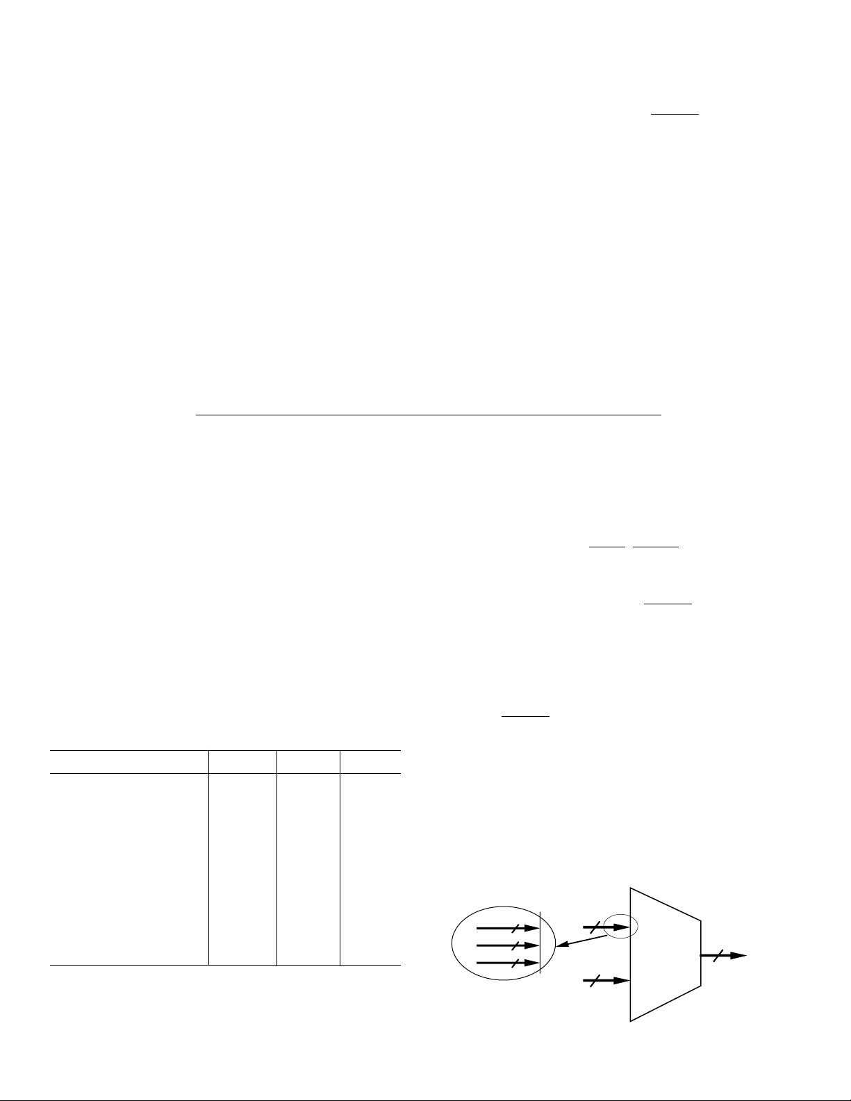
The ADV7152 has 48 color data inputs. The part has two (for
2:1 multiplexing) 24-bit wide direct color data inputs. These
are user programmed to support a number of color data formats including 24-Bit True Color, 15-Bit True Color and
8-Bit Pseudo Color (see “Color Data Formats” section) in 2:1
and 1:1 multiplex modes.
RED
GREEN
BLUE
8
8
8
24
A
MULTIPLEXER
24
B
24
–10–
Figure 10. Multiplexed Color Inputs for the ADV7152
REV. B
 Loading...