192-Bit, 360 MHz True-Color
a
FEATURES
192-Bit Pixel Port Allows 2048 3 2048 3 24 Screen
Resolution
360 MHz, 24-Bit True-Color Operation
Triple 8-Bit D/A Converters
8:1 Multiplexing
Onboard PLL
RS-343A/RS-170 Compatible Analog Outputs
TTL Compatible Digital Inputs
Internal Voltage Reference
Standard 8-Bit MPU I/O Interface
DAC-DAC Matching: Typ 2%, Adjustable to 0.02%
+5 V CMOS Monolithic Construction
304-Pin PQFP Package
APPLICATIONS
Ultrahigh Resolution Color Graphics
Image Processing
Drives 24-Bit Color 2K 3 2K Monitors
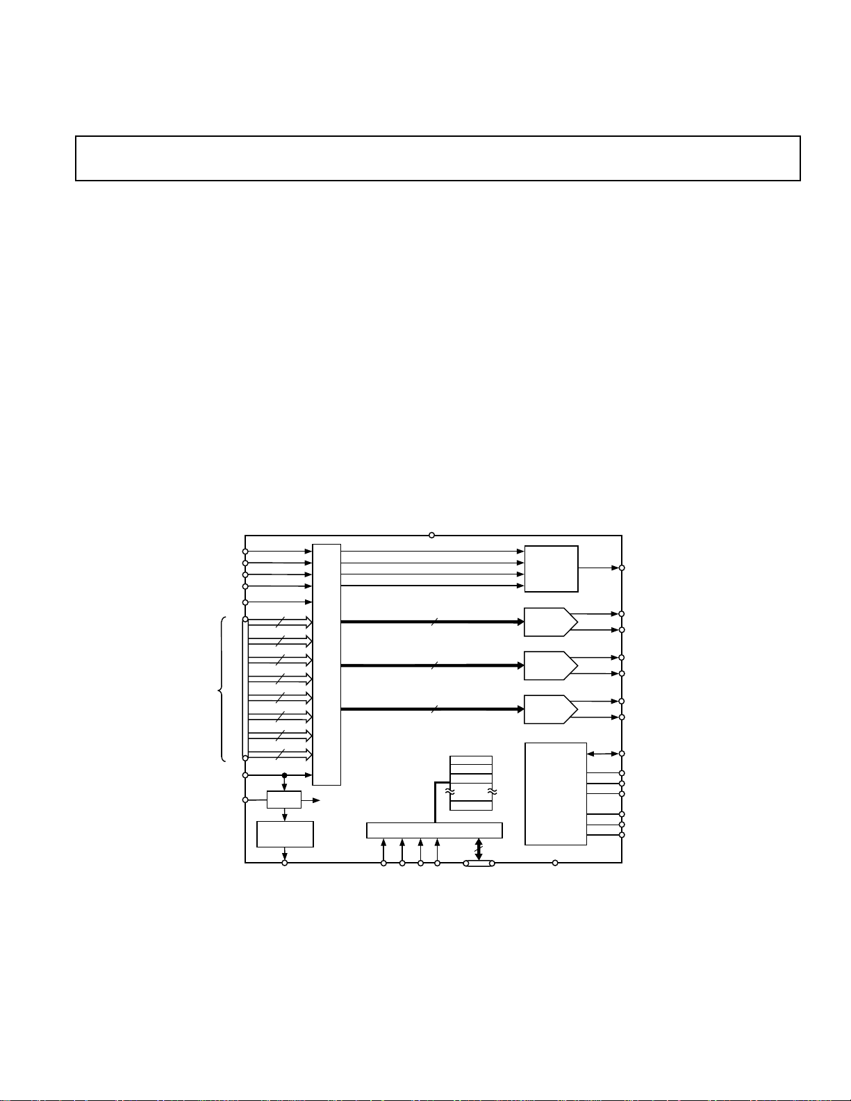
FUNCTIONAL BLOCK DIAGRAM
Video DAC with Onboard PLL
ADV7129
GENERAL DESCRIPTION
The ADV7129 is a complete analog output, video DAC on a single
CMOS (ADV®) monolithic chip. The part is specifically designed
for use in the highest resolution graphics and imaging systems.
The ultimate level of integration, comprised of 360 MHz triple
8-bit DACs, a programmable pixel port, an internal voltage reference and an onboard PLL, makes the ADV7129 the only choice
for the very highest level of performance and functionality.
The device consists of three high speed, 8-bit, video D/A converters (RGB). An onboard phase locked loop clock generator
is provided to provide high speed operation without requiring
high speed external crystal or clock circuitry.
The part is fully controlled through the MPU port by the onboard command registers. This MPU port may be updated at
any time without causing sparkle effects on the screen.
ADV is a registered trademark of Analog Devices, Inc.
(continued on page 10)
V
AA
VSYNC
HSYNC
CSYNC
BLANK
ODD/EVEN
PIXEL
DATA
(RED,
GREEN,
BLUE)
LOADIN
LPF
ADV is a registered trademark of Analog Devices, Inc..
24
A
24
B
24
C
24
D
24
E
24
F
24
G
24
H
CLOCK
CONTROL
LOADOUT
MUX
PLL
8:1
INT PIXEL
CLOCK
ADV7129
CONTROL
REGISTERS
8
8
8
MPU PORT
BLANK
AND SYNC
LOGIC
RED
DAC
GREEN
DAC
BLUE
DAC
VOLTAGE
REFERENCE
8
D7–D0CE R/W C0 C1
GND
SENSE/SYNCOUT
IOR
IOR
IOG
IOG
IOB
IOB
V
REF
R
RSET
R
GSET
R
BSET
RCOMP
GCOMP
BCOMP
REV. 0
Information furnished by Analog Devices is believed to be accurate and
reliable. However, no responsibility is assumed by Analog Devices for its
use, nor for any infringements of patents or other rights of third parties
which may result from its use. No license is granted by implication or
otherwise under any patent or patent rights of Analog Devices.
One Technology Way, P.O. Box 9106, Norwood, MA 02062-9106, U.S.A.
Tel: 617/329-4700 World Wide Web Site: http://www.analog.com
Fax: 617/326-8703 © Analog Devices, Inc., 1996

1
(V
ADV7129–SPECIFICATIONS
All specifications T
All Versions Conditions
STATIC PERFORMANCE
3
= +5 V, V
AA
1
= +1.235 V, R
REF
to T
MIN
, R
RSET
GSET, RBSET
unless otherwise noted.)
MAX
2
= 280 V, RL = 25 V, CL = 10 pF.
Min Typ Max Units
Resolution (Each DAC) 8 Bits
Accuracy (Each DAC)
Integral Nonlinearity ± 1 LSB
Differential Nonlinearity Guaranteed Monotonic ± 1 LSB
Gray Scale Error ±5 % Gray Scale
Binary Coding
DIGITAL INPUTS
Input High Voltage, V
Input Low Voltage, V
Input Current, I
Input Capacitance, C
INL
IN
IN
INH
V
= 0.4 V or 2.4 V ±10 µA
IN
2.0 VAA + 0.5 V
GND – 0.5 0.8 V
10 pF
DIGITAL OUTPUTS
Output High Voltage, V
Output Low Voltage, V
OL
OH
I
= –400 µA 2.4 V
OH
IOL = 3.2 mA 0.4 V
Floating-State Leakage Current ±10 µA
Floating-State Output Capacitance 10 pF
ANALOG OUTPUTS
Gray Scale Current Range 10 60 mA
Output Current
White Level Relative to Black 50.16 52.80 55.44 mA
Black Level Relative to Blank 4.1 4.32 4.54 mA
Blank Level, Sync Disabled 0 5 50 µA
LSB Size 223 µA
DAC to DAC Matching 2 5 %
Output Compliance, V
Output Impedance, R
OC
OUT
Output Capacitance, C
OUT
0 1.4 V
10 kΩ
20 pF
VOLTAGE REFERENCE
Voltage Reference Range, V
Input Current, I
VREF
REF
V
= 1.234 V for Specified 1.14 1.235 1.30 V
REF
Performance 5 µA
POWER REQUIREMENTS
V
AA
4
I
AA
4
I
AA
Analog Current 160 200 mA
Digital Current @ 360 MHz 360 400 mA
5V
Power Supply Rejection Ratio 0.12 %/%
DYNAMIC PERFORMANCE
Clock and Data Feedthrough
Glitch Impulse 50 pV secs
DAC to DAC Crosstalk
NOTES
1
±5%
for all versions.
2
Temperature range (T
3
Static performance is measured with the Gain Error Registers set to 00H (disabled).
4
IAA is measured with a typical dynamic pattern, satisfying the absolute maximum current spec for the DACs.
5
Clock and Data Feedthrough is a function of the amount of overshoot and undershoot on the digital inputs. Glitch impulse includes clock and data
feedthrough. TTL input values are 0 V to 3 V, with input rise/fall times ≥3 ns, measured at the 10% and 90% points. Timing reference points are at 50% for
inputs and outputs.
6
DAC to DAC crosstalk is measured by holding one DAC high while the other two DACs are making low to high and high to low transitions.
Specifications subject to change without notice.
MIN
to T
5
6
), 0°C to +70°C, TJ (Silicon Junction Temperature) ≤100oC.
MAX
–2–
–30 dB
–23 dB
REV. 0

ADV7129
2
(V
= +5 V, V
TIMING SPECIFICATIONS
AA
All specifications T
Parameter Conditions Min Typ Max Units
CLOCK CONTROL & PIXEL PORT
LOADIN Clocking Rate, f
LOADIN Cycle Time, t
LOADIN Low Time, t
LOADIN High Time, t
LCLK
1
2
3
LOADIN to LOADOUT Delay, t
Pixel Setup Time, t
Pixel Hold Time, t
5
6
4
4
MPU PORT
R/
W, C0, C1 Setup Time, t
R/
W, C0, C1 Hold Time, t
CE Low Time, t
CE High Time, t
9
10
CE Asserted to Data-Bus Driven, t
CE Asserted to Data-Bus Valid, t
CE Negated to Data-Bus Invalid, t
CE Negated to Data-Bus Three Stated, t
Write Data (D7–D0) Setup Time, t
Write Data (D7–D0) Hold Time, t
ANALOG OUTPUTS
Analog Output Delay, t
Analog Output Rise/Fall Time, t
Analog Output Transition Time, t
RGB Analog Output Skew, t
Pipeline Delay, t
PD
PLL PERFORMANCE
7
8
11
12
13
14
15
16
5
17
18
19
SK
6
Jitter (1σ) (LOADIN = 45 MHz) 55 ps rms
NOTES
1
TTL inputs values are 0 V to 3 V with input rise/fall times ≥3 ns, measured between the 10% and 90% points. Timing reference points at 50% for inputs and outputs. Analog output load ≤10 pF. Databus (D7–D0) loaded as shown in Figure 1. Digital output load for SENSE ≤30 pF.
2
±5% for all versions.
3
Temperature range (T
4
Pixel Port consists of the following inputs: Pixel Inputs: RED [A-H], BLUE [A-H], GREEN [A-H].
5
Output Delay is measured from the 50% rising edge of LOADIN to the 50% point of full-scale transition on the A pixel. t17 includes the analog delay due to DACs
and internal gate transitions plus the pipeline stages delay. The output delay for pixels B-H will be the output delay to the A pixel (t17) plus the appropriate number
of clock cycles. Output rise/fall time is measured between the 10% and 90% points of full-scale transition. Settling time is measured from the 50% point of full-scale
transition to the output remaining within 1%. (Settling Time does not include clock and data feedthrough.)
6
Jitter is measured by triggering on the output clock, delayed by 15 µs and then measuring the time period from the trigger edge to the next edge of the output clock
after the delay. This measurement is repeated multiple times and the rms value is determined.
Specifications subject to change without notice.
MIN
to T
MAX
), 0°C to +70°C.
= +1.235 V, R
REF
to T
MIN
MAX
, R
RSET
3
GSET, RBSET
unless otherwise noted.)
= 280 V, RL = 25 V for IOG, IOR, IOB, CL = 10 pF.
10 45 MHz
16.67 ns
6.67 ns
6.67 ns
5ns
10 ns
42 ns
10 2.5 ns
10 0.5 ns
25 ns
25 ns
25 ns
20 ns
1ns
15 ns
10 ns
10 ns
@ 360 MHz 5 ns
0.8 ns
25 ns
1.5 ns
19 PCLKs
REV. 0
I
SINK
TO OUTPUT PIN +2.1V
100pF
I
SOURCE
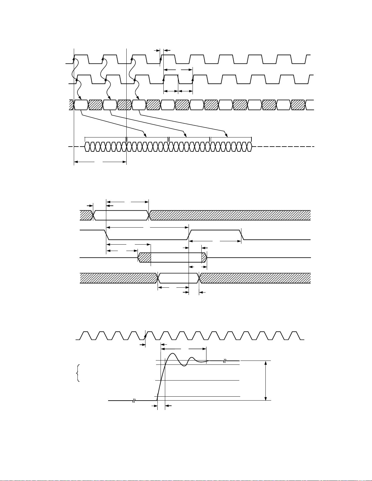
Figure 1. LOADIN vs. Pixel Input Data
–3–

ADV7129
LOADOUT
LOADIN
t
4
t
1
t2 t
3
PIXEL
INPUT
DATA
ANALOG
OUTPUT
DATA
R/W, C0, C1
D7–D0
(READ MODE)
D7–D0
(WRITE MODE)
AN ...
H
N
DIGITAL INPUT TO ANALOG
OUTPUT PIPELINE
CE
A
... H
N–1
t
PD
t
7
A
N+1
H
N+1
N–1
CONTROL DATA
...
A
...
N+2
H
N+2
A
AN ... H
N
N+1
... H
N+1
Figure 2. LOADIN vs. Pixel Input Data
t
8
VALID
t
9
t
12
t
11
R/W = 1
R/W = 0
t
15
t
13
t
t
16
A
... H
N+2
N+2
t
10
14
Figure 3. Microprocessor Port (MPU) Interface Timing
PCLK
t
17
IOR
ANALOG
OUTPUTS
NOTE:
THIS DIAGRAM IS NOT TO SCALE.
FOR THE PURPOSES OF CLARITY, THE ANALOG OUTPUT WAVEFORM IS MAGNIFIED IN TIME AND AMPLITUDE W.R.T THE CLOCK WAVEFORM.
SYNCOUT IS A DIGITAL VIDEO OUTPUT SIGNAL.
t
17
IOG
IOB
SYNCOUT
t
18
IS THE ONLY RELEVENT TIMING SPECIFICATION FOR SYNCOUT.
t
19
WHITE LEVEL
90 %
50 %
10 %
FULL-SCALE
TRANSITION
BLACK LEVEL
Figure 4. Analog Output Response vs. LOADIN
–4–
REV. 0

ADV7129
77
152
PIN NO. 1 IDENTIFIER
1
304
76
153228
229
ROW A
ROW BROW D
ADV7129
PQFP
TOP VIEW
(Not to Scale)
ROW C
WARNING!
ESD SENSITIVE DEVICE
ABSOLUTE MAXIMUM RATINGS
V
to GND . . . . . . . . . . . . . . . . . . . . . . . . . . . . . . . . . . . . . 7 V
AA
Voltage on Any Digital Pin . . . . GND – 0.5 V to V
Ambient Operating Temperature (T
Storage Temperature (T
Junction Temperature (T
) . . . . . . . . . . . . . . –65°C to +150°C
S
) . . . . . . . . . . . . . . . . . . . . . +150°C
J
1
+ 0.5 V
) . . . . . . . . 0°C to +70°C
A
AA
Lead Temperature (Soldering, 10 sec) . . . . . . . . . . . . . +260°C
Vapor Phase Soldering (1 minute) . . . . . . . . . . . . . . . . +220°C
Analog Outputs to GND
2
. . . . . . . . . . . GND – 0.5 V to V
AA
Current on Any DAC Output . . . . . . . . . . . . . . . . . . . . 60 mA
NOTES
1
Stresses above those listed under “Absolute Maximum Ratings” may cause
permanent damage to the device. This is a stress rating only and functional
operation of the device at these or any other conditions above those listed in the
operational sections of this specification is not implied. Exposure to absolute
maximum rating conditions for extended periods may affect device reliability.
2
Analog Output Short Circuit to any Power Supply or Common can be of an
indefinite duration.
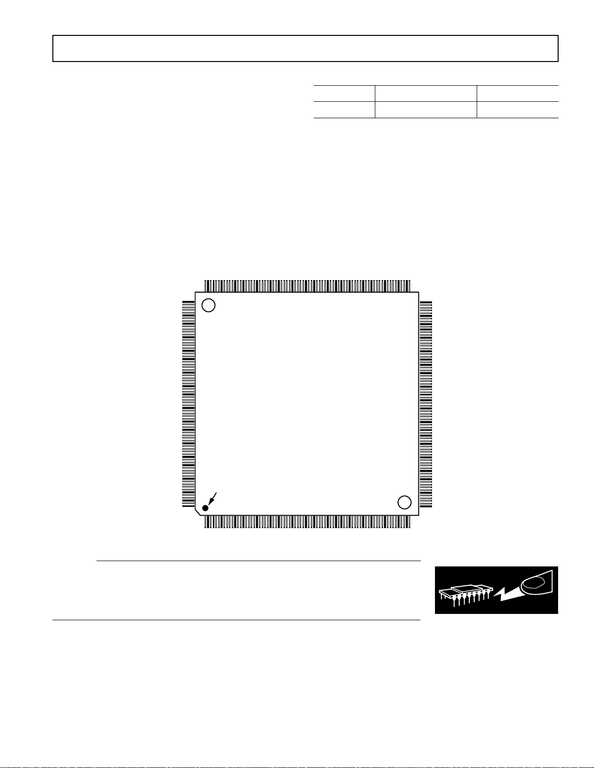
304-LEAD PQFP PIN CONFIGURATION
ORDERING GUIDE*
Model Temperature Range Package Option
ADV7129KS 0°C to +70°C S-304
*Due to the specialized nature and application of this part, it is not automati-
cally available to order. Please contact your local sales office for details.
CAUTION
ESD (electrostatic discharge) sensitive device. Electrostatic charges as high as 4000 V readily
accumulate on the human body and test equipment and can discharge without detection.
Although the ADV7129 features proprietary ESD protection circuitry, permanent damage may
occur on devices subjected to high energy electrostatic discharges. Therefore, proper ESD
precautions are recommended to avoid performance degradation or loss of functionality.
REV. 0
–5–

ADV7129
PIN ASSIGNMENTS
Pin No. Mnemonic Pin No. Mnemonic Pin No. Mnemonic Pin No. Mnemonic
1 GND 41 G4
2 GND 42 G4
3 GND 43 G4
4 GND 44 V
C
B
A
AA
81 GND 121 B4
82 GND 122 B4
83 G1
84 G0
5 GND 45 GND 85 G0
6 GND 46 V
7R0
8R0
9R0
10 R0
11 R0
12 G7
13 G7
14 G7
15 G7
16 G7
17 G7
18 G7
19 G7
20 G6
21 G6
22 G6
23 G6
24 G6
25 G6
26 G6
27 G6
28 G5
29 G5
30 G5
31 G5
32 G5
33 G5
34 G5
35 G5
36 G4
37 G4
38 G4
39 G4
40 G4
*No Connect.
E
D
C
B
A
H
G
F
E
D
C
B
A
H
G
F
E
D
C
B
A
H
G
F
E
D
C
B
A
H
G
F
E
D
47 GND 87 G0
48 G3
49 G3
50 G3
51 G3
52 G3
53 G3
54 G3
55 G3
56 G2
57 G2
58 G2
59 G2
60 G2
61 G2
62 G2
63 G2
64 G1
65 G1
66 G1
67 G1
68 G1
69 G1
70 G1
71 GND 111 B5
72 GND 112 B5
73 GND 113 B5
74 GND 114 B5
75 GND 115 B5
76 GND 116 V
77 GND 117 GND 157 GND
78 GND 118 B4
79 GND 119 B4
80 GND 120 B4
AA
H
G
F
E
D
C
B
A
H
G
F
E
D
C
B
A
H
G
F
E
D
C
B
86 G0
88 G0
89 G0
90 G0
91 G0
92 B7
93 B7
94 B7
95 B7
96 B7
97 B7
98 B7
99 B7
100 B6
101 B6
102 B6
103 B6
104 B6
105 B6
106 B6
107 B6
108 B5
109 B5
110 B5
AA
E
A
H
G
F
E
D
C
B
A
H
G
F
E
D
C
B
A
H
G
F
E
D
C
B
A
H
G
F
E
D
C
B
A
123 B4
124 B4
125 B4
126 B3
127 B3
128 B3
129 B3
130 B3
131 B3
132 B3
133 B3
134 B2
135 B2
136 B2
137 B2
138 B2
139 B2
140 B2
141 B2
142 B1
143 B1
144 B1
145 B1
146 B1
147 GND
148 GND
149 GND
150 GND
151 GND
152 GND
153 GND
154 GND
155 GND
D
C
B
A
H
G
F
E
D
C
B
A
H
G
F
E
D
C
B
A
H
G
F
E
D
156 GND
H
G
F
158 GND
159 B1
160 B1
C
B
–6–
REV. 0
 Loading...