Analog Devices ADV7127 Datasheet
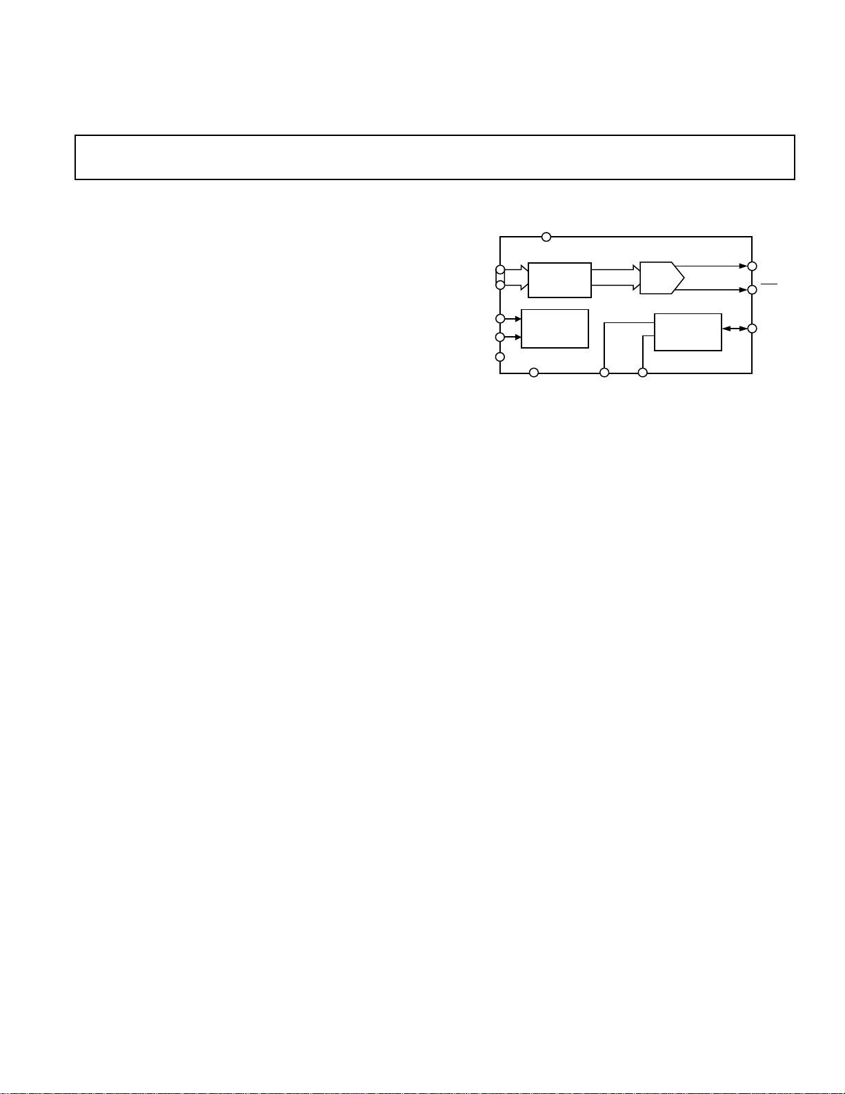
CMOS, 240 MHz
D9–D0
GND R
SET
I
OUT
I
OUT
COMP
ADV7127
V
REF
VOLTAGE*
REFERENCE
CIRCUIT
PDOWN*
POWER–
DOWN
MODE
V
AA
10
DAC
10
DATA
REGISTER
CLOCK
PSAVE
*ON TSSOP VERSION ONLY
a
FEATURES
240 MSPS Throughput Rate
10-Bit D/A Converters
SFDR
–70 dB typ: f
–53 dB typ: f
RS-343A/RS-170 Compatible Output
Complementary Outputs
DAC Output Current Range: 2 mA to 26 mA
TTL Compatible Inputs
Internal Voltage Reference (1.23 V) on TSSOP Package
Single Supply +5 V/+3.3 V Operation
28-Lead SOIC Package and 24-Lead TSSOP Package
Low Power Dissipation (30 mW min @ 3 V)
Low Power Standby Mode (10 mW min @ 3 V)
Power-Down Mode (60 mW min @ 3 V)
Power-Down Mode Available on TSSOP Package
Industrial Temperature Range (–408C to +858C)
APPLICATIONS
Digital Video Systems (1600 3 1200 @ 100 Hz)
High Resolution Color Graphics
Digital Radio Modulation
Image Processing
Instrumentation
Video Signal Reconstruction
Direct Digital Synthesis (DDS)
Wireless LAN
= 50 MHz; f
CLK
= 140 MHz; f
CLK
= 1 MHz
OUT
= 40 MHz
OUT
10-Bit High Speed Video DAC
ADV7127
FUNCTIONAL BLOCK DIAGRAM
GENERAL DESCRIPTION
The ADV7127 (ADV®) is a high speed, digital-to-analog convertor on a single monolithic chip. It consists of a 10-bit,
video D/A converter with on-board voltage reference, complementary outputs, a standard TTL input interface and high
impedance analog output current sources.
The ADV7127 has a 10-bit wide input port. A single +5 V/
+3.3 V power supply and clock are all that are required to make
the part functional.
The ADV7127 is fabricated in a CMOS process. Its monolithic
CMOS construction ensures greater functionality with lower
power dissipation. The ADV7127 is available in a small outline
28-lead SOIC or 24-lead TSSOP package.
ADV is a registered trademark of Analog Devices, Inc.
REV. 0
Information furnished by Analog Devices is believed to be accurate and
reliable. However, no responsibility is assumed by Analog Devices for its
use, nor for any infringements of patents or other rights of third parties
which may result from its use. No license is granted by implication or
otherwise under any patent or patent rights of Analog Devices.
The ADV7127 TSSOP package also has a power-down mode.
Both ADV7127 packages have a power standby mode.
The ADV7127 TSSOP package has an on-board voltage reference circuit. The ADV7127 SOIC package requires an external
reference.
PRODUCT HIGHLIGHTS
1. 240 MSPS Throughput.
2. Guaranteed monotonic to 10 bits.
3. Compatible with a wide variety of high resolution color
graphics systems including RS-343A and RS-170A.
One Technology Way, P.O. Box 9106, Norwood, MA 02062-9106, U.S.A.
Tel: 781/329-4700 World Wide Web Site: http://www.analog.com
Fax: 781/326-8703 © Analog Devices, Inc., 1998

ADV7127–SPECIFICATIONS
(VAA = +5 V 6 5%, V
5 V SOIC SPECIFICATIONS
otherwise noted, TJ
Parameter Min Typ Max Units Test Conditions
STATIC PERFORMANCE
Resolution (Each DAC) 10 Bits
Integral Nonlinearity (BSL) –1 0.4 +1 LSB
Differential Nonlinearity –1 0.25 +1 LSB Guaranteed Monotonic
DIGITAL AND CONTROL INPUTS
Input High Voltage, V
Input Low Voltage, V
Input Current, I
IL
IN
IH
2V
–1 +1 µAV
PSAVE Pull-Up Current 20 µA
Input Capacitance, C
IN
ANALOG OUTPUTS
Output Current 2.0 18.5 mA
Output Compliance Range, V
Output Impedance, R
OUT
Output Capacitance, C
Offset Error –0.025 +0.025 % FSR Tested with DAC Output = 0 V
Gain Error
2
OC
OUT
0 +1.4 V
–5.0 +5.0 % FSR FSR = 17.62 mA
VOLTAGE REFERENCE (Ext.)
Reference Range, V
REF
POWER DISSIPATION
Digital Supply Current
Digital Supply Current
Digital Supply Current
3
3
3
1.12 1.235 1.35 V
Analog Supply Current 33 37 mA R
Analog Supply Current 5 mA R
Standby Supply Current
4
Power Supply Rejection Ratio 0.1 0.5 %/%
NOTES
1
Temperature range T
2
Gain error = ((Measured (FSC)/Ideal (FSC) –1) × 100), where Ideal = V
3
Digital supply is measured with continuous clock with data input corresponding to a ramp pattern and with an input level at 0 V and VDD.
4
These max/min specifications are guaranteed by characterization to be over 4.75 V to 5.25 V range.
Specifications subject to change without notice.
MIN
to T
: –40°C to +85°C at 50 MHz and 140 MHz, 0°C to +70° C at 240 MHz.
MAX
= 1.235 V, R
REF
= 1108C)
MAX
= 560 V, CL = 10 pF. All specifications T
SET
MIN
to T
MAX1
0.8 V
= 0.0 V or V
IN
AA
10 pF
100 kΩ
10 pF I
3.4 9 mA f
10.5 15 mA f
18 25 mA f
= 0 mA
OUT
= 50 MHz
CLK
= 140 MHz
CLK
= 240 MHz
CLK
= 560 Ω
SET
= 4933 Ω
SET
2.1 5.0 mA PSAVE = Low, Digital and Control
× K × (3FFH) and K = 7.9896.
REF /RSET
Inputs at V
AA
unless
–2– REV. 0

ADV7127
(VAA = +5 V 6 5%, V
5 V TSSOP SPECIFICATIONS
otherwise noted, TJ
Parameter Min Typ Max Units Test Conditions
STATIC PERFORMANCE
Resolution (Each DAC) 10 Bits
Integral Nonlinearity (BSL) –1 0.4 +1 LSB
Differential Nonlinearity –1 0.25 +1 LSB Guaranteed Monotonic
DIGITAL AND CONTROL INPUTS
Input High Voltage, V
Input Low Voltage, V
PDOWN Input High Voltage
PDOWN Input Low Voltage
Input Current, I
IH
IL
2
2
IN
2V
–1 +1 µAV
PSAVE Pull-Up Current 20 µA
PDOWN Pull-Up Current 20 µA
Input Capacitance, C
IN
ANALOG OUTPUTS
Output Current 2.0 18.5 mA
Output Compliance Range, V
Output Impedance, R
OUT
Output Capacitance, C
Offset Error –0.025 +0.025 % FSR Tested with DAC Output = 0 V
Gain Error
3
OC
OUT
VOLTAGE REFERENCE (Ext. and Int.)
Reference Range, V
POWER DISSIPATION
Digital Supply Current
Digital Supply Current
Digital Supply Current
REF
5
5
5
0 +1.4 V
–5.0 +5.0 % FSR FSR = 17.62 mA
4
1.12 1.235 1.35 V
Analog Supply Current 23 27 mA R
Analog Supply Current 5 mA R
Standby Supply Current
PDOWN Supply Current
6
2
Power Supply Rejection Ratio 0.1 0.5 %/%
NOTES
1
Temperature range T
2
This power-down feature is only available on the ADV7127 in the TSSOP package.
3
Gain error = ((Measured (FSC)/Ideal (FSC) –1) × 100), where Ideal = V
4
Internal voltage reference is available only on the ADV7127 TSSOP package.
5
Digital supply is measured with continuous clock with data input corresponding to a ramp pattern and with an input level at 0 V and VDD.
6
These max/min specifications are guaranteed by characterization to be over 4.75 V to 5.25 V range.
Specifications subject to change without notice.
MIN
to T
: –40°C to +85°C at 50 MHz and 140 MHz, 0°C to +70° C at 240 MHz.
MAX
= 1.235 V, R
REF
= 1108C)
MAX
= 560 V, CL = 10 pF. All specifications T
SET
MIN
to T
MAX1
0.8 V
3V
1V
= 0.0 V or V
IN
AA
10 pF
100 kΩ
10 pF I
1.5 3 mA f
46 mA f
6.5 10 mA f
= 0 mA
OUT
= 50 MHz
CLK
= 140 MHz
CLK
= 240 MHz
CLK
= 560 Ω
SET
= 4933 Ω
SET
3.8 6 mA PSAVE = Low, Digital and Control
Inputs at V
AA
1mA
× K × (3FFH ) and K = 7.9896.
REF /RSET
unless
–3–REV. 0

ADV7127–SPECIFICATIONS
(VAA = +3.0 V–3.6 V, V
3.3 V SOIC SPECIFICATIONS
1
unless otherwise noted, TJ
Parameter Min Typ Max Units Test Conditions
STATIC PERFORMANCE
Resolution (Each DAC) 10 Bits R
Integral Nonlinearity (BSL) –1 0.5 +1 LSB R
Differential Nonlinearity –1 0.25 +1 LSB R
DIGITAL AND CONTROL INPUTS
Input High Voltage, V
Input Low Voltage, V
Input Current, I
IL
IN
IH
2.0 V
0.8 V
–1 +1 µAV
PSAVE Pull-Up Current 20 µA
Input Capacitance, C
IN
10 pF
ANALOG OUTPUTS
Output Current 2.0 18.5 mA
Output Compliance Range, V
Output Impedance, R
OUT
Output Capacitance, C
Offset Error 0 0 % FSR Tested with DAC Output = 0 V
Gain Error
3
OC
OUT
0 +1.4 V
70 kΩ
10 pF
0 % FSR FSR = 17.62 mA
VOLTAGE REFERENCE (Ext.)
Reference Range, V
POWER DISSIPATION
Digital Supply Current
Digital Supply Current
Digital Supply Current
REF
4
4
4
1.12 1.235 1.35 V
2.2 5.0 mA f
6.5 12.0 mA f
11 15 mA f
Analog Supply Current 32 35 mA R
Analog Supply Current 5 mA R
Standby Supply Current 2.4 5.0 mA PSAVE = Low, Digital and Control
Power Supply Rejection Ratio 0.1 0.5 %/%
NOTES
1
These max/min specifications are guaranteed by characterization to be over 3.0 V to 3.6 V range.
2
Temperature range T
3
Gain error = ((Measured (FSC)/Ideal (FSC) –1) × 100) , where Ideal = V
4
Digital supply is measured with continuous clock with data input corresponding to a ramp pattern and with an input level at 0 V and VDD.
Specifications subject to change without notice.
MIN
to T
: –40°C to +85°C at 50 MHz and 140 MHz, 0°C to +70° C at 240 MHz.
MAX
REF /RSET
= 1.235 V, R
REF
= 1108C)
MAX
× K × (3FFH) and K = 7.9896.
= 560 V, CL = 10 pF. All specifications T
SET
= 680 Ω
SET
= 680 Ω
SET
= 680 Ω
SET
= 0.0 V or V
IN
= 50 MHz
CLK
= 140 MHz
CLK
= 240 MHz
CLK
= 560 Ω
SET
= 4933 Ω
SET
Inputs at V
DD
DD
MIN
to T
MAX
2
–4– REV. 0

ADV7127
(VAA = +3.0 V–3.6 V, V
3.3 V TSSOP SPECIFICATIONS
1
unless otherwise noted, TJ
Parameter Min Typ Max Units Test Conditions
STATIC PERFORMANCE
Resolution (Each DAC) 10 Bits R
Integral Nonlinearity (BSL) –1 0.5 +1 LSB R
Differential Nonlinearity –1 0.25 +1 LSB R
DIGITAL AND CONTROL INPUTS
Input High Voltage, V
Input Low Voltage, V
PDOWN Input High Voltage
PDOWN Input Low Voltage
Input Current, I
IH
IL
IN
3
3
2.0 V
0.8 V
2.1 V
0.6 V
–1 +1 µAV
PSAVE Pull-Up Current 20 µA
Input Capacitance, C
IN
10 pF
ANALOG OUTPUTS
Output Current 2.0 18.5 mA
Output Compliance Range, V
Output Impedance, R
OUT
Output Capacitance, C
Offset Error 0 0 % FSR Tested with DAC Output = 0 V
Gain Error
4
OC
OUT
0 +1.4 V
70 kΩ
10 pF
0 % FSR FSR = 17.62 mA
VOLTAGE REFERENCE (Ext.)
Reference Range, V
VOLTAGE REFERENCE (Int.)
Reference Range, V
POWER DISSIPATION
Digital Supply Current
Digital Supply Current
Digital Supply Current
REF
5
REF
6
6
6
1.12 1.235 1.35 V
1.235 V
12 mA f
2.5 4.5 mA f
46 mA f
Analog Supply Current 22 25 mA R
Analog Supply Current 5 mA R
Standby Supply Current 2.6 3 mA PSAVE = Low, Digital and Control
PDOWN Supply Current 20 µA
Power Supply Rejection Ratio 0.1 0.5 %/%
NOTES
1
These max/min specifications are guaranteed by characterization to be over 3.0 V to 3.6 V range.
2
Temperature range T
3
This power-down feature is only available on the ADV7127 in the TSSOP package.
4
Gain error = ((Measured (FSC)/Ideal (FSC) –1) × 100), where Ideal = V
5
Internal voltage reference is available only on the ADV7127 TSSOP package.
6
Digital supply is measured with continuous clock with data input corresponding to a ramp pattern and with an input level at 0 V and VDD.
Specifications subject to change without notice.
MIN
to T
: –40°C to +85°C at 50 MHz and 140 MHz, 0°C to +70° C at 240 MHz.
MAX
REF /RSET
= 1.235 V, R
REF
= 1108C)
MAX
× K × (3FFH) and K = 7.9896.
= 560 V, CL = 10 pF. All specifications T
SET
= 680 Ω
SET
= 680 Ω
SET
= 680 Ω
SET
= 0.0 V or V
IN
= 50 MHz
CLK
= 140 MHz
CLK
= 240 MHz
CLK
= 560 Ω
SET
= 4933 Ω
SET
Inputs at V
DD
DD
MIN
to T
MAX
2
–5–REV. 0
 Loading...