CMOS, 170 MHz, Triple, 10-Bit
V
FEATURES
170 MSPS throughput rate
Triple, 10-bit digital-to-analog converters (DACs)
SFDR
−70 dB at f
−53 dB at f
RS-343A-/RS-170-compatible output
Complementary outputs
DAC output current range: 2.0 mA to 26.5 mA
TTL-compatible inputs
Internal reference: 1.235 V
Single-supply 3.3 V operation
48-lead LFCSP package
Low power dissipation: 30 mW minimum at 3 V
Low power standby mode: 6 mW typical at 3 V
Supports defense and aerospace applications
(AQEC standard)
Military temperature range: −55°C to +105°C
Controlled manufacturing baseline
One assembly/test site
One fabrication site
Enhanced product change notification
Qualification data available on request
APPLICATIONS
Digital video systems
High resolution color graphics
Digital radio modulation
Image processing
Instrumentation
Video signal reconstruction
= 50 MHz; f
CLK
= 140 MHz; f
CLK
= 1 MHz
OUT
= 40 MHz
OUT
High Speed Video DAC
ADV7123-EP
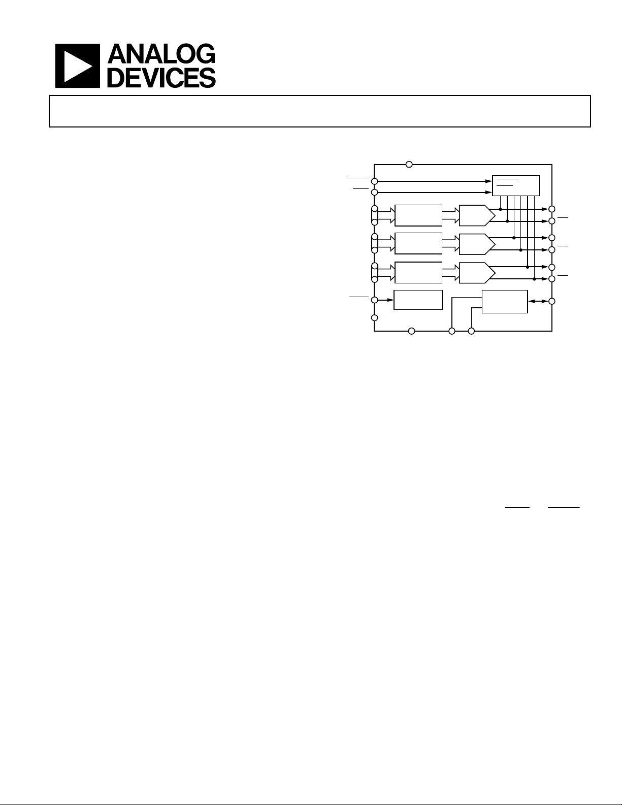
FUNCTIONAL BLOCK DIAGRAM
AA
BLANK
SYNC
DATA
R9 TO R0
G9 TO G0
B9 TO B0
PSAVE
CLOCK
10
REGISTER
10
REGISTER
10
REGISTER
POWER-DOWN
DATA
DATA
MODE
10
10
10
R
COMPGND
SET
Figure 1.
GENERAL DESCRIPTION
The ADV7123-EP is a triple, high speed digital-to-analog
converter (DAC) on a single monolithic chip. It consists of three
high speed, 10-bit video DACs with complementary outputs,
a standard TTL input interface, and a high impedance, analog
output current source.
The ADV7123-EP has three separate 10-bit-wide input ports.
A single 3.3 V power supply and clock are the only components
required to make the part functional. The ADV7123-EP has
additional video control signals: composite
The ADV7123-EP also has a power save mode.
The ADV7123-EP is fabricated in a 5 V CMOS process. Its
monolithic CMOS construction ensures greater functionality
with lower power dissipation. The ADV7123-EP is available
in a 48-lead LFCSP package.
Full details about this enhanced product are available in the
ADV7123 data sheet, which should be consulted in conjunction
with this data sheet.
PRODUCT HIGHLIGHTS
1. Guaranteed monotonic to 10 bits.
2. Compatible with a wide variety of high resolution color
graphics systems, including RS-343A and RS-170.
DAC
DAC
DAC
REFERENCE
BLANK AND
SYNC LOGIC
VOLTAGE
CIRCUIT
ADV7123-EP
SYNC
and
IOR
IOR
IOG
IOG
IOB
IOB
V
REF
BLANK
09200-001
.
Rev. 0
Information furnished by Analog Devices is believed to be accurate and reliable. However, no
responsibility is assumed by Analog Devices for its use, nor for any infringements of patents or other
rights of third parties that may result from its use. Specifications subject to change without notice. No
license is granted by implication or otherwise under any patent or patent rights of Analog Devices.
Trademarks and registered trademarks are the property of their respective owners.
One Technology Way, P.O. Box 9106, Norwood, MA 02062-9106, U.S.A.
Tel: 781.329.4700 www.analog.com
Fax: 781.461.3113 ©2010 Analog Devices, Inc. All rights reserved.

ADV7123-EP
TABLE OF CONTENTS
Features .............................................................................................. 1
Applications ....................................................................................... 1
Functional Block Diagram .............................................................. 1
General Description ......................................................................... 1
Product Highlights ........................................................................... 1
Revision History ............................................................................... 2
Specifications ..................................................................................... 3
Dynamic Specifications ............................................................... 4
REVISION HISTORY
7/10—Revision 0: Initial Version
Timing Specifications ...................................................................5
Absolute Maximum Ratings ............................................................7
ESD Caution...................................................................................7
Pin Configuration and Function Descriptions ..............................8
Outline Dimensions ....................................................................... 10
Ordering Guide .......................................................................... 10
Rev. 0 | Page 2 of 12

ADV7123-EP
SPECIFICATIONS
VAA = 3.0 V to 3.6 V, V
Table 1.
Parameter
2
STATIC PERFORMANCE
Resolution (Each DAC) 10 Bits R
Integral Nonlinearity (BSL) −1 +0.5 +1 LSB R
Differential Nonlinearity −1 +0.25 +1 LSB R
DIGITAL AND CONTROL INPUTS
Input High Voltage, VIH 2.0 V
Input Low Voltage, VIL 0.8 V
Input Current, IIN −1 +1 μA VIN = 0.0 V or VDD
PSAVE Pull-Up Current
Input Capacitance, CIN 10 pF
ANALOG OUTPUTS
Output Current 2.0 26.5 mA
DAC-to-DAC Matching 1.0 %
Output Compliance Range, VOC 0 1.4 V
Output Impedance, R
Output Capacitance, C
Offset Error 0 0 % FSR Tested with DAC output = 0 V
Gain Error
3
VOLTAGE REFERENCE, EXTERNAL
Reference Range, V
VOLTAGE REFERENCE, INTERNAL
Voltage Reference, V
POWER DISSIPATION
Digital Supply Current
6.5 12.0 mA f
7.5 13.5 mA f
Analog Supply Current 67 72 mA R
8 mA R
Standby Supply Current 2.1 5.0 mA
Power Supply Rejection Ratio 0.1 0.5 %/%
1
Temperature range T
2
These maximum/minimum specifications are guaranteed by characterization over the 3.0 V to 3.6 V range.
3
Gain error = {(Measured (FSC)/Ideal (FSC) − 1) × 100}, where Ideal (FSC) = V
4
Digital supply is measured with a continuous clock that has data input corresponding to a ramp pattern and with an input level at 0 V and VDD.
= 1.235 V, R
REF
= 560 Ω, CL = 10 pF. All specifications T
SET
MIN
to T
,1 unless otherwise noted; T
MAX
Min Typ Max Unit Test Conditions/Comments
= 680 Ω
SET
= 680 Ω
SET
= 680 Ω
SET
20 μA
Green DAC, SYNC
2.0 18.5 mA
70 kΩ
OUT
10 pF
OUT
RGB DAC, SYNC
0 % FSR FSR = 17.62 mA
1.12 1.235 1.35 V
REF
1.235 V
REF
4
to T
MIN
: −55°C to +105°C.
MAX
2.2 5.0 mA f
× K × (0x3FFH) and K = 7.9896.
REF/RSET
= 50 MHz
CLK
= 140 MHz
CLK
= 170 MHz
CLK
= 560 Ω
SET
= 4933 Ω
SET
= low, digital and control inputs at VDD
PSAVE
= high
= low
J MAX
1
= 110°C.
Rev. 0 | Page 3 of 12

ADV7123-EP
DYNAMIC SPECIFICATIONS
VAA = 3.0 V to 3.6 V, V
= 1.235 V, R
REF
= 680 Ω, CL = 10 pF. All specifications are at TA = 25°C, unless otherwise noted; T
SET
J MAX
= 110°C.
Table 2.
Parameter
1
Min Typ Max Unit
AC LINEARITY
Spurious-Free Dynamic Range to Nyquist
2
Single-Ended Output
f
= 50 MHz; f
CLK
f
= 50 MHz; f
CLK
f
= 50 MHz; f
CLK
f
= 50 MHz; f
CLK
f
= 100 MHz; f
CLK
f
= 100 MHz; f
CLK
f
= 100 MHz; f
CLK
f
= 100 MHz; f
CLK
f
= 140 MHz; f
CLK
f
= 140 MHz; f
CLK
f
= 140 MHz; f
CLK
f
= 140 MHz; f
CLK
= 1.00 MHz 67 dBc
OUT
= 2.51 MHz 67 dBc
OUT
= 5.04 MHz 63 dBc
OUT
= 20.2 MHz 55 dBc
OUT
= 2.51 MHz 62 dBc
OUT
= 5.04 MHz 60 dBc
OUT
= 20.2 MHz 54 dBc
OUT
= 40.4 MHz 48 dBc
OUT
= 2.51 MHz 57 dBc
OUT
= 5.04 MHz 58 dBc
OUT
= 20.2 MHz 52 dBc
OUT
= 40.4 MHz 41 dBc
OUT
Double-Ended Output
f
= 50 MHz; f
CLK
f
= 50 MHz; f
CLK
f
= 50 MHz; f
CLK
f
= 50 MHz; f
CLK
f
= 100 MHz; f
CLK
f
= 100 MHz; f
CLK
f
= 100 MHz; f
CLK
f
= 100 MHz; f
CLK
f
= 140 MHz; f
CLK
f
= 140 MHz; f
CLK
f
= 140 MHz; f
CLK
f
= 140 MHz; f
CLK
= 1.00 MHz 70 dBc
OUT
= 2.51 MHz 70 dBc
OUT
= 5.04 MHz 65 dBc
OUT
= 20.2 MHz 54 dBc
OUT
= 2.51 MHz 67 dBc
OUT
= 5.04 MHz 63 dBc
OUT
= 20.2 MHz 58 dBc
OUT
= 40.4 MHz 52 dBc
OUT
= 2.51 MHz 62 dBc
OUT
= 5.04 MHz 61 dBc
OUT
= 20.2 MHz 55 dBc
OUT
= 40.4 MHz 53 dBc
OUT
Spurious-Free Dynamic Range Within a Window
Single-Ended Output
f
= 50 MHz; f
CLK
f
= 50 MHz; f
CLK
f
= 140 MHz; f
CLK
= 1.00 MHz; 1 MHz Span 77 dBc
OUT
= 5.04 MHz; 2 MHz Span 73 dBc
OUT
= 5.04 MHz; 4 MHz Span 64 dBc
OUT
Double-Ended Output
f
= 50 MHz; f
CLK
f
= 50 MHz; f
CLK
f
= 140 MHz; f
CLK
= 1.00 MHz; 1 MHz Span 74 dBc
OUT
= 5.00 MHz; 2 MHz Span 73 dBc
OUT
= 5.00 MHz; 4 MHz Span 60 dBc
OUT
Total Harmonic Distortion
f
= 50 MHz; f
CLK
= 1.00 MHz
OUT
TA = 25°C 66 dBc
T
to T
MIN
f
= 50 MHz; f
CLK
f
= 100 MHz; f
CLK
f
= 140 MHz; f
CLK
65 dBc
MAX
= 2.00 MHz 64 dBc
OUT
= 2.00 MHz 64 dBc
OUT
= 2.00 MHz 55 dBc
OUT
Rev. 0 | Page 4 of 12
 Loading...