CMOS, 240 MHz
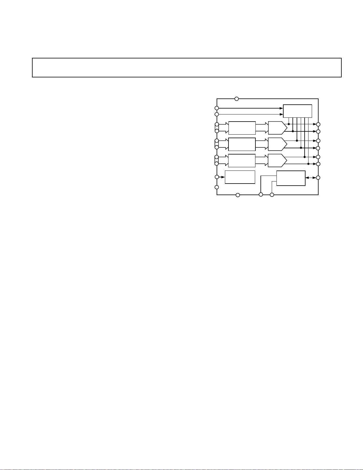
R9–R0
GND
R
SET
IOR
IOR
COMP
ADV7123
V
REF
VOLTAGE
REFERENCE
CIRCUIT
G9–G0
B9–B0
IOG
IOG
IOB
IOB
PSAVE
POWER-DOWN
MODE
BLANK
SYNC
CLOCK
V
AA
DAC10
DATA
REGISTER
10
DAC10
DATA
REGISTER
10
DAC10
DATA
REGISTER
10
BLANK AND
SYNC LOGIC
a
Triple 10-Bit High Speed Video DAC
FEATURES
240 MSPS Throughput Rate
Triple 10-Bit D/A Converters
SFDR
–70 dB at f
–53 dB at f
= 50 MHz; f
CLK
= 140 MHz; f
CLK
= 1 MHz
OUT
= 40 MHz
OUT
RS-343A/RS-170 Compatible Output
Complementary Outputs
DAC Output Current Range 2 mA to 26 mA
TTL-Compatible Inputs
Internal Reference (1.23 V)
Single Supply +5 V/+3.3 V Operation
48-Lead LQFP Package
Low Power Dissipation (30 mW min @ 3 V)
Low Power Standby Mode (6 mW typ @ 3 V)
Industrial Temperature Range (–408C to +858C)
APPLICATIONS
Digital Video Systems (1600 3 1200 @ 100 Hz)
High Resolution Color Graphics
Digital Radio Modulation
Image Processing
Instrumentation
Video Signal Reconstruction
GENERAL DESCRIPTION
The ADV7123 (ADV®) is a triple high speed, digital-to-analog
converter on a single monolithic chip. It consists of three
high speed, 10-bit, video D/A converters with complementary
outputs, a standard TTL input interface and a high impedance,
analog output current source.
The ADV7123 has three separate 10-bit-wide input ports. A
single +5 V/+3.3 V power supply and clock are all that are
required to make the part functional. The ADV7123 has additional video control signals, composite SYNC and BLANK.
The ADV7123 also has a power-save mode.
The ADV7123 is fabricated in a +5 V CMOS process. Its
monolithic CMOS construction ensures greater functionality
with lower power dissipation. The ADV7123 is available in a
48-lead LQFP package.
ADV7123
FUNCTIONAL BLOCK DIAGRAM
PRODUCT HIGHLIGHTS
1. 240 MSPS Throughput.
2. Guaranteed monotonic to 10 bits.
3. Compatible with a wide variety of high resolution color
graphics systems including RS-343A and RS-170A.
ADV is a registered trademark of Analog Devices, Inc.
REV. A
Information furnished by Analog Devices is believed to be accurate and
reliable. However, no responsibility is assumed by Analog Devices for its
use, nor for any infringements of patents or other rights of third parties
which may result from its use. No license is granted by implication or
otherwise under any patent or patent rights of Analog Devices.
One Technology Way, P.O. Box 9106, Norwood, MA 02062-9106, U.S.A.
Tel: 781/329-4700 World Wide Web Site: http://www.analog.com
Fax: 781/326-8703 © Analog Devices, Inc., 1998

ADV7123–SPECIFICATIONS
to T
1
DD
MAX
1
unless
5 V SPECIFICATIONS
(VAA = +5 V 6 5%, V
otherwise noted, TJ
= 1.235 V, R
REF
= 1108C)
MAX
= 560 V, CL = 10 pF. All specifications T
SET
MIN
Parameter Min Typ Max Units Test Conditions
STATIC PERFORMANCE
Resolution (Each DAC) 10 Bits
Integral Nonlinearity (BSL) –1 ±0.4 +1 LSB
Differential Nonlinearity –1 ±0.25 +1 LSB Guaranteed Monotonic
DIGITAL AND CONTROL INPUTS
Input High Voltage, V
Input Low Voltage, V
Input Current, I
IL
IN
IH
2V
0.8 V
–1 +1 µAV
= 0.0 V or V
IN
PSAVE Pull-Up Current 20 µA
Input Capacitance, C
IN
10 pF
ANALOG OUTPUTS
Output Current 2.0 26.5 mA Green DAC, Sync = High
Output Current 2.0 18.5 mA R/G/B DAC, Sync = Low
DAC to DAC Matching 1.0 5 %
Output Compliance Range, V
Output Impedance, R
OUT
Output Capacitance, C
Offset Error –0.025 +0.025 % FSR Tested with DAC Output = 0 V
Gain Error
2
OC
OUT
0 +1.4 V
100 kΩ
10 pF I
OUT
= 0 mA
–5.0 +5.0 % FSR FSR = 17.62 mA
VOLTAGE REFERENCE (Ext. and Int.)
Reference Range, V
POWER DISSIPATION
Digital Supply Current
Digital Supply Current
Digital Supply Current
REF
3
3
3
Analog Supply Current 67 72 mA R
Analog Supply Current 8 mA R
Standby Supply Current
4
1.12 1.235 1.35 V
3.4 9 mA f
10.5 15 mA f
18 25 mA f
2.1 5.0 mA PSAVE = Low, Digital and Control
= 50 MHz
CLK
= 140 MHz
CLK
= 240 MHz
CLK
= 560 Ω
SET
= 4933 Ω
SET
Inputs at V
DD
Power Supply Rejection Ratio 0.1 0.5 %/%
NOTES
1
Temperature range T
2
Gain error = (Measured (FSC)/Ideal (FSC) –1) × 100), where Ideal = V
3
Digital supply is measured with continuous clock with data input corresponding to a ramp pattern and with an input level at 0 V and VDD.
4
These max/min specifications are guaranteed by characterization to be over 4.75 V to 5.25 V range.
Specifications subject to change without notice.
MIN
to T
: –40°C to +85°C at 50 MHz and 140 MHz, 0°C to 70°C at 240 MHz.
MAX
/R
× K × (3FFH) and K = 7.9896.
REF
SET
–2–
REV. A

ADV7123
(VAA = +3.0 V –3.6 V, V
3.3 V SPECIFICATIONS
1
otherwise noted, TJ
Parameter Min Typ Max Units Test Conditions
REF
= 1108C)
MAX
= 1.235 V, R
= 560 V, CL = 10 pF. All specifications T
SET
MIN
2
STATIC PERFORMANCE
Resolution (Each DAC) 10 Bits R
Integral Nonlinearity (BSL) –1 0.5 +1 LSB R
Differential Nonlinearity –1 0.25 +1 LSB R
= 680 Ω
SET
= 680 Ω
SET
= 680 Ω
SET
DIGITAL AND CONTROL INPUTS
Input High Voltage, V
Input Low Voltage, V
Input Current, I
IL
IN
IH
2.0 V
0.8 V
–1 +1 µAV
= 0.0 V or V
IN
DD
PSAVE Pull-Up Current 20 µA
Input Capacitance, C
IN
10 pF
ANALOG OUTPUTS
Output Current 2.0 26.5 mA Green DAC, Sync = High
Output Current 2.0 18.5 mA R/G/B DAC, Sync = Low
DAC to DAC Matching 1.0 %
Output Compliance Range, V
Output Impedance, R
OUT
Output Capacitance, C
Offset Error 0 0 % FSR Tested with DAC Output = 0 V
Gain Error
3
OC
OUT
0 +1.4 V
70 kΩ
10 pF
0 % FSR FSR = 17.62 mA
VOLTAGE REFERENCE (Ext.)
Reference Range, V
REF
1.12 1.235 1.35 V
VOLTAGE REFERENCE (Int.)
Reference Range, V
POWER DISSIPATION
Digital Supply Current
Digital Supply Current
Digital Supply Current
REF
4
4
4
Analog Supply Current 67 72 mA R
Analog Supply Current 8 mA R
1.235 V
2.2 5.0 mA f
6.5 12.0 mA f
11 15 mA f
= 50 MHz
CLK
= 140 MHz
CLK
= 240 MHz
CLK
= 560 Ω
SET
= 4933 Ω
SET
Standby Supply Current 2.1 5.0 mA PSAVE = Low, Digital and Control
Inputs at V
DD
Power Supply Rejection Ratio 0.1 0.5 %/%
NOTES
1
These max/min specifications are guaranteed by characterization to be over 3.0 V to 3.6 V range.
2
Temperature range T
3
Gain error = (Measured (FSC)/Ideal (FSC) –1) × 100), where Ideal = V
4
Digital supply is measured with continuous clock with data input corresponding to a ramp pattern and with an input level at 0 V and VDD.
Specifications subject to change without notice.
MIN
to T
: –40°C to +85°C at 50 MHz and 140 MHz, 0°C to 70°C at 240 MHz.
MAX
/R
× K × (3FFH) and K = 7.9896.
REF
SET
to T
MAX
2
unless
–3–REV. A

ADV7123–SPECIFICATIONS
(VAA = +5 V 6 5%1, V
5 V DYNAMIC SPECIFICATIONS
1
TA = +258C unless otherwise noted, TJ
Parameter Min Typ Max Units
AC LINEARITY
Spurious-Free Dynamic Range to Nyquist
2
Single-Ended Output
f
= 50 MHz; f
CLK
f
= 50 MHz; f
CLK
f
= 50 MHz; f
CLK
f
= 50 MHz; f
CLK
f
= 100 MHz; f
CLK
f
= 100 MHz; f
CLK
f
= 100 MHz; f
CLK
f
= 100 MHz; f
CLK
f
= 140 MHz; f
CLK
f
= 140 MHz; f
CLK
f
= 140 MHz; f
CLK
f
= 140 MHz; f
CLK
= 1.00 MHz 67 dBc
OUT
= 2.51 MHz 67 dBc
OUT
= 5.04 MHz 63 dBc
OUT
= 20.2 MHz 55 dBc
OUT
= 2.51 MHz 62 dBc
OUT
= 5.04 MHz 60 dBc
OUT
= 20.2 MHz 54 dBc
OUT
= 40.4 MHz 48 dBc
OUT
= 2.51 MHz 57 dBc
OUT
= 5.04 MHz 58 dBc
OUT
= 20.2 MHz 52 dBc
OUT
= 40.4 MHz 41 dBc
OUT
Double-Ended Output
f
= 50 MHz; f
CLK
f
= 50 MHz; f
CLK
f
= 50 MHz; f
CLK
f
= 50 MHz; f
CLK
f
= 100 MHz; f
CLK
f
= 100 MHz; f
CLK
f
= 100 MHz; f
CLK
f
= 100 MHz; f
CLK
f
= 140 MHz; f
CLK
f
= 140 MHz; f
CLK
f
= 140 MHz; f
CLK
f
= 140 MHz; f
CLK
= 1.00 MHz 70 dBc
OUT
= 2.51 MHz 70 dBc
OUT
= 5.04 MHz 65 dBc
OUT
= 20.2 MHz 54 dBc
OUT
= 2.51 MHz 67 dBc
OUT
= 5.04 MHz 63 dBc
OUT
= 20.2 MHz 58 dBc
OUT
= 40.4 MHz 52 dBc
OUT
= 2.51 MHz 62 dBc
OUT
= 5.04 MHz 61 dBc
OUT
= 20.2 MHz 55 dBc
OUT
= 40.4 MHz 53 dBc
OUT
Spurious-Free Dynamic Range Within a Window
Single-Ended Output
f
= 50 MHz; f
CLK
f
= 50 MHz; f
CLK
f
= 140 MHz; f
CLK
= 1.00 MHz; 1 MHz Span 77 dBc
OUT
= 5.04 MHz; 2 MHz Span 73 dBc
OUT
= 5.04 MHz; 4 MHz Span 64 dBc
OUT
Double-Ended Output
f
= 50 MHz; f
CLK
f
= 50 MHz; f
CLK
f
= 140 MHz; f
CLK
= 1.00 MHz; 1 MHz Span 74 dBc
OUT
= 5.00 MHz; 2 MHz Span 73 dBc
OUT
= 5.00 MHz; 4 MHz Span 60 dBc
OUT
Total Harmonic Distortion
f
= 50 MHz; f
CLK
T
= +25°C 66 dBc
A
T
to T
MIN
f
= 50 MHz; f
CLK
f
= 100 MHz; f
CLK
f
= 140 MHz; f
CLK
MAX
= 1.00 MHz
OUT
= 2.00 MHz 64 dBc
OUT
= 2.00 MHz 63 dBc
OUT
= 2.00 MHz 55 dBc
OUT
DAC PERFORMANCE
Glitch Impulse 10 pVs
DAC Crosstalk
Data Feedthrough
Clock Feedthrough
NOTES
1
These max/min specifications are guaranteed by characterization over 4.75 V to 5.25 V range.
2
Note that the ADV7123 exhibits high performance when operating with an internal voltage reference, V
3
DAC to DAC Crosstalk is measured by holding one DAC high while the other two are making low to high and high to low transitions.
4
Clock and data feedthrough is a function of the amount of overshoot and undershoot on the digital inputs. Glitch impulse includes clock and data feedthrough.
5
TTL input values are 0 V to 3 V, with input rise/fall times ≤3 ns, measured the 10% and 90% points. Timing reference points is 50% for inputs and outputs.
Specifications subject to change without notice.
3
4, 5
4, 5
= 1.235 V, R
REF
= 560 V, CL = 10 pF. All specifications are for
SET
= 1108C)
MAX
65 dBc
23 dB
22 dB
33 dB
.
REF
–4–
REV. A

ADV7123
(VAA = +3.0 V–3.6 V1, V
3.3 V DYNAMIC SPECIFICATIONS
TA = +258C unless otherwise noted, TJ
Parameter Min Typ Max Units
AC LINEARITY
Spurious-Free Dynamic Range to Nyquist
2
Single-Ended Output
f
= 50 MHz; f
CLK
f
= 50 MHz; f
CLK
f
= 50 MHz; f
CLK
f
= 50 MHz; f
CLK
f
= 100 MHz; f
CLK
f
= 100 MHz; f
CLK
f
= 100 MHz; f
CLK
f
= 100 MHz; f
CLK
f
= 140 MHz; f
CLK
f
= 140 MHz; f
CLK
f
= 140 MHz; f
CLK
f
= 140 MHz; f
CLK
= 1.00 MHz 67 dBc
OUT
= 2.51 MHz 67 dBc
OUT
= 5.04 MHz 63 dBc
OUT
= 20.2 MHz 55 dBc
OUT
= 2.51 MHz 62 dBc
OUT
= 5.04 MHz 60 dBc
OUT
= 20.2 MHz 54 dBc
OUT
= 40.4 MHz 48 dBc
OUT
= 2.51 MHz 57 dBc
OUT
= 5.04 MHz 58 dBc
OUT
= 20.2 MHz 52 dBc
OUT
= 40.4 MHz 41 dBc
OUT
Double-Ended Output
f
= 50 MHz; f
CLK
f
= 50 MHz; f
CLK
f
= 50 MHz; f
CLK
f
= 50 MHz; f
CLK
f
= 100 MHz; f
CLK
f
= 100 MHz; f
CLK
f
= 100 MHz; f
CLK
f
= 100 MHz; f
CLK
f
= 140 MHz; f
CLK
f
= 140 MHz; f
CLK
f
= 140 MHz; f
CLK
f
= 140 MHz; f
CLK
= 1.00 MHz 70 dBc
OUT
= 2.51 MHz 70 dBc
OUT
= 5.04 MHz 65 dBc
OUT
= 20.2 MHz 54 dBc
OUT
= 2.51 MHz 67 dBc
OUT
= 5.04 MHz 63 dBc
OUT
= 20.2 MHz 58 dBc
OUT
= 40.4 MHz 52 dBc
OUT
= 2.51 MHz 62 dBc
OUT
= 5.04 MHz 61 dBc
OUT
= 20.2 MHz 55 dBc
OUT
= 40.4 MHz 53 dBc
OUT
Spurious-Free Dynamic Range Within a Window
Single-Ended Output
f
= 50 MHz; f
CLK
f
= 50 MHz; f
CLK
f
= 140 MHz; f
CLK
= 1.00 MHz; 1 MHz Span 77 dBc
OUT
= 5.04 MHz; 2 MHz Span 73 dBc
OUT
= 5.04 MHz; 4 MHz Span 64 dBc
OUT
Double-ended Output
f
= 50 MHz; f
CLK
f
= 50 MHz; f
CLK
f
= 140 MHz; f
CLK
= 1.00 MHz; 1 MHz Span 74 dBc
OUT
= 5.00 MHz; 2 MHz Span 73 dBc
OUT
= 5.00 MHz; 4 MHz Span 60 dBc
OUT
Total Harmonic Distortion
f
= 50 MHz; f
CLK
T
= +25°C 66 dBc
A
T
to T
MIN
f
= 50 MHz; f
CLK
f
= 100 MHz; f
CLK
f
= 140 MHz; f
CLK
MAX
= 1.00 MHz
OUT
= 2.00 MHz 64 dBc
OUT
= 2.00 MHz 64 dBc
OUT
= 2.00 MHz 55 dBc
OUT
DAC PERFORMANCE
Glitch Impulse 10 pVs
DAC Crosstalk
Data Feedthrough
Clock Feedthrough
NOTES
1
These max/min specifications are guaranteed by characterization over 3.0 V to 3.6 V range.
2
Note that the ADV7123 exhibits high performance when operating with an internal voltage reference, V
3
DAC to DAC Crosstalk is measured by holding one DAC high while the other two are making low to high and high to low transitions.
4
Clock and data feedthrough is a function of the amount of overshoot and undershoot on the digital inputs. Glitch impulse includes clock and data feedthrough.
5
TTL input values are 0 V to 3 V, with input rise/fall times ≤3 ns, measured the 10% and 90% points. Timing reference points is 50% for inputs and outputs.
Specifications subject to change without notice.
3
4, 5
4, 5
= 1.235 V, R
REF
= 680 V, CL = 10 pF. All specifications are
SET
= 1108C)
MAX
65 dBc
23 dB
22 dB
33 dB
.
REF
–5–REV. A
 Loading...