CMOS Monolithic 256318
a
FEATURES
Personal System/2* and VGA* Compatible
Plug-in Replacement for INMOS 171/176
66 MHz Pipelined Operation
Three 6-Bit D/A Converters
256318 Color Palette RAM
RS-343A/RS-170 Compatible Outputs
Blank on All Three Channels
Standard MPU Interface
Asynchronous Access to All Internal Registers
15 V CMOS Monolithic Construction
Low Power Dissipation
Standard 28-Pin, 0.6" DIP and 44-Pin PLCC
APPLICATIONS
High Resolution Color Graphics
CAE/CAD/CAM Applications
Image Processing
Instrumentation
Desktop Publishing
AVAILABLE CLOCK RATES
66 MHz
50 MHz
35 MHz
Color Palette RAM-DAC
ADV476
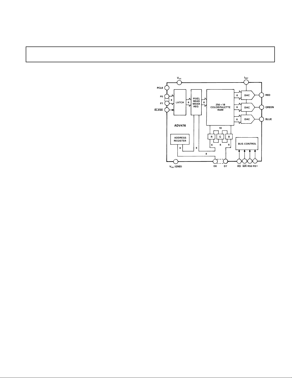
FUNCTIONAL BLOCK DIAGRAM
GENERAL DESCRIPTION
The ADV476 (ADV®) is a pin compatible and software compatible RAM-DAC designed specifically for VGA and Personal
System/2 color graphics.
The ADV476 is a complete analog output RAM-DAC on a
single monolithic chip. The part contains a 256318 color
lookup table, a pixel mask register as well as a triple 6-bit video
D/A converter. The ADV476 is capable of simultaneously displaying up to 256 colors, from a total color palette of 262,144
addressable colors.
The on-chip asynchronous MPU bus allows access to the color
lookup table without affecting the input video data via the pixel
port. The pixel read mask register provides a convenient way of
altering the displayed colors without updating the color lookup
table. The ADV476 is capable of generating RGB video output
signals which are compatible with RS-343A and RS-170 video
standards, without requiring external buffering.
*Personal System/2 and VGA are trademarks of International Business
Machines Corp.
ADV is a registered trademark of Analog Devices, Inc.
REV. B
Information furnished by Analog Devices is believed to be accurate and
reliable. However, no responsibility is assumed by Analog Devices for its
use, nor for any infringements of patents or other rights of third parties
which may result from its use. No license is granted by implication or
otherwise under any patent or patent rights of Analog Devices.
The ADV476 is fabricated in a +5 V CMOS process. Its monolithic CMOS construction ensures greater functionality with low
power dissipation and small board area. The part is packaged in
a 0.6", 28-pin DIP and a 44-pin PLCC.
PRODUCT HIGHLIGHTS
1. Standard video refresh rates, 35 MHz, 50 MHz and
66 MHz.
2. Fully compatible with VGA and Personal System/2 color
graphics.
3. Guaranteed monotonic. Integral and differential linearity
guaranteed to be a maximum of ±1 LSB.
4. Low glitch energy, 75 pV secs.
One Technology Way, P.O. Box 9106, Norwood, MA 02062-9106, U.S.A.
Tel: 617/329-4700 Fax: 617/326-8703

ADV476–SPECIFICA TIONS
(VCC = +5 V 6 10%, I
All Specifications T
MIN
REF
to T
= 8.88 mA.
1
unless otherwise noted.)
MAX
Parameter All Versions Units Test Conditions/Comments
STATIC PERFORMANCE
Resolution (Each DAC) 6 Bits
Accuracy (Each DAC)
Integral Nonlinearity ±0.5 LSB max Guaranteed Monotonic
Full Scale Error ±5 % max Full Scale = 2.15 3 I
Blank Level ±0.5 LSB max
BLANK = Logic Low
REF
3 RL, I
Offset Error ±0.5 LSB max BLANK = Logic High
DIGITAL INPUTS
Input High Voltage, V
Input Low Voltage, V
Input Current, I
INL
IN
INH
2 V min
0.8 V max
±10 µA max VCC = 5.5 V, VIN = 0.4 V to V
Input Current (RD Input Only) ±100 µA max VCC = 5.5 V, VIN = 0.4 V to V
Input Capacitance, C
IN
7 pF typ
DIGITAL OUTPUTS
Output High Voltage, V
Output Low Voltage, V
OH
OL
Floating-State Leakage Current ±50 µA max V
2.4 V min I
0.4 V max I
= 500 µA, VCC = 4.5 V
SOURCE
= 5.0 mA, VCC = 4.5 V
SINK
= 5.5 V, 0.4 V < VIN < V
CC
CC
Floating-State Output Capacitance 7 pF typ
ANALOG OUTPUTS
Max Output Voltage 1.5 V min IO < 10 mA, IO = 2.15 3 I
Max Output Current 21 mA min VO ≤ 1 V
DAC to DAC Matching
2
±2.5 % max
REF
Analog Output Capacitance 10 pF typ BLANK = Logic Low
= 8.39 mA
REF
CC
CC
CURRENT REFERENCE
Input Current (I
Voltage at I
REF
) Range –3/–10 mA min/mA max
REF
VCC –3/V
V min/V max I
CC
= 8.88 mA
REF
POWER SUPPLY
Supply Voltage, V
Supply Current, I
CC
CC
Power Supply Rejection Ratio 6 %/V 4.5 < V
DYNAMIC PERFORMANCE
Clock and Data Feedthrough
Glitch Impulse
NOTES
1
Temperature range (T
2
Relative to the midpoint of the distribution of the three DACs measured at full scale.
3
TTL input values are 0 to 3 volts, with input rise/fall times ≤3 ns, measured between the 10% and 90% points. Timing reference points at 50% for inputs and outputs. Analog output load ≤10 pF, 37.5 Ω. D0–D7 output load ≤ 50 pF. See timing notes in Figure 2.
4
Clock and data feedthrough is a function of the amount of overshoot and undershoot on the digital inputs. For this test, the digital inputs have a 1 k Ω resistor to
ground and are driven by 74HC logic. Glitch impulse includes clock and data feedthrough, –3 dB test bandwidth = 2 3 clock rate.
Specifications subject to change without notice.
3, 4
MIN
to T
3, 4
); 0 to +70°C.
MAX
4.5/5.5 V min/V max
220 mA max f
–35 dB typ
75 pV secs typ
= 66 MHz IO = 2.15 3 I
MAX
CL = 30 pF, I
< 5.5 V, IO = 2.15 3 I
CC
= 8.88 mA.
REF
, D0–D7 Unloaded
REF
, RL = 37.5 Ω,
REF
–2–
REV. B

ADV476
TIMING CHARACTERISTICS
1
(VCC = +5 V 6 10%. All Specifications T
MIN
to T
MAX
2
)
Parameter 66 MHz Version 50 MHz Version 35 MHz Version Units Conditions/Comments
f
MAX
t
1
t
2
t
3
t
4
t
5
t
6
t
7
t
8
t
9
t
10
t
11
t
12
t
13
t
14
t
15
66 50 35 MHz Clock Rate
10 10 15 ns min RS0, RS1 Setup Time
10 10 15 ns min RS0, RS1 Hold Time
5 5 5 ns min RD Asserted to Data Bus Driven
40 40 40 ns max RD Asserted to Data Valid
20 20 20 ns max RD Negated to Data Bus 3-Stated
10 10 15 ns min Write Data Setup Time
10 10 15 ns min Write Data Hold Time
50 50 50 ns min RD, WR Pulse Width Low
43t
12
43t
12
43t
12
ns min RD, WR Pulse Width High
3 3 4 ns min Pixel & Control Setup Time
3 3 4 ns min Pixel & Control Hold Time
15.3 20 28 ns min Clock Cycle Time
5 6 7 ns min Clock Pulse Width High Time
5 6 9 ns min Clock Pulse Width Low Time
30 30 30 ns max Analog Output Delay
5 5 5 ns min
t
16
3
t
17
t
18
t
PD
NOTES
1
TTL input values are 0 to 3 volts, with input rise/fall times ≤3 ns, measured between the 10% and 90% points. Timing reference points at 50% for inputs and
outputs. Analog output load ≤10 pF, 37.5 Ω. D0–D7 output load ≤50 pF. See timing notes in Figure 2.
2
Temperature Range (T
3
Settling time does not include clock and data feedthrough. For this test, the digital inputs have a 1 kΩ resistor to ground and are driven by 74HC logic.
Specifications subject to change without notice.
6 8 8 ns max Analog Output Rise/Fall Time
15.3 20 25 ns typ Analog Output Settling Time
2 2 2 ns min Analog Output Skew
4 4 4 clocks Pipeline Delay
to T
MIN
); 0 to +70°C
MAX
REV. B
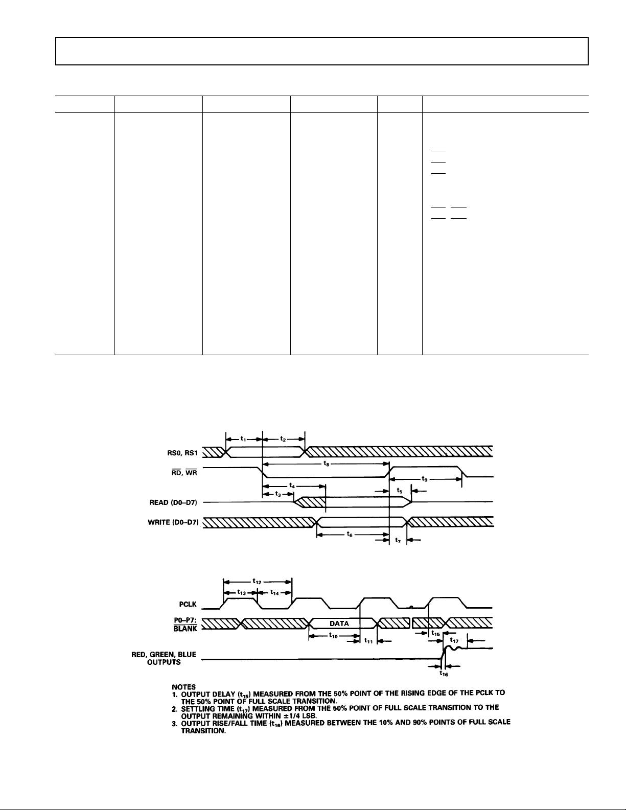
Figure 1. MPU Read/Write Timing
Figure 2. Video Input/Output Timing
–3–

ADV476
ABSOLUTE MAXIMUM RATINGS
1
ORDERING GUIDE
VCC to GND . . . . . . . . . . . . . . . . . . . . . . . . . . . . . . . . . . +7 V
Voltage on any Digital Pin . . . . . GND – 0.5 V to V
Ambient Operating Temperature (T
Storage Temperature (T
Junction Temperature (T
) . . . . . . . . . . . . . . –65°C to +150°C
S
) . . . . . . . . . . . . . . . . . . . . +150°C
J
) . . . . . –55°C to +125°C
A
Lead Temperature (Soldering, 10 secs) . . . . . . . . . . . +300°C
Vapor Phase Soldering (1 minute) . . . . . . . . . . . . . . . +220°C
Red, Green, Blue to GND
NOTES
1
Stresses above those listed under “Absolute Maximum Ratings” may cause
permanent damage to the device. This is a stress rating only and functional
operation of the device at these or any other conditions above those listed in the
operational sections of this specification is not implied. Exposure to absolute
maximum rating conditions for extended periods may affect device reliability.
2
Analog output short circuit to any power supply or common can be of an indefinite
duration.
2
. . . . . . . . . . . . . . . . . . 0 V to V
+ 0.5 V
CC
Model Speed Package Type Option
ADV476KN35 35 MHz 28-Pin DIP N-28
ADV476KN50 50 MHz 28-Pin DIP N-28
ADV476KN66 66 MHz 28-Pin DIP N-28
ADV476KP35 35 MHz 44-Pin PLCC P-44A
ADV476KP50 50 MHz 44-Pin PLCC P-44A
CC
ADV476KP66 66 MHz 44-Pin PLCC P-44A
NOTES
1
All devices are specified for 0°C to +70°C operation.
2
Devices are packaged in 0.6" 28-pin plastic DIPs (N-28), and 44-pin J-leaded
PLCC (P-44A).
3
N = Plastic DIP; P = Plastic Leaded Chip Carrier.
RECOMMENDED OPERATING CONDITIONS
Parameter Symbol Min Typ Max Units
Power Supply V
Ambient Operating Temperature T
Output Load R
Reference Current I
CC
A
L
REF
4.5 5.00 5.5 Volts
0 +70 °C
37.5 Ω
–3 –10 mA
CAUTION
ESD (electrostatic discharge) sensitive device. Electrostatic charges as high as 4000 V readily
accumulate on the human body and test equipment and can discharge without detection.
Although the ADV476 features proprietary ESD protection circuitry, permanent damage may
occur on devices subjected to high energy electrostatic discharges. Therefore, proper ESD
precautions are recommended to avoid performance degradation or loss of functionality.
1, 2
WARNING!
ESD SENSITIVE DEVICE
Package
3
PLCC DIP
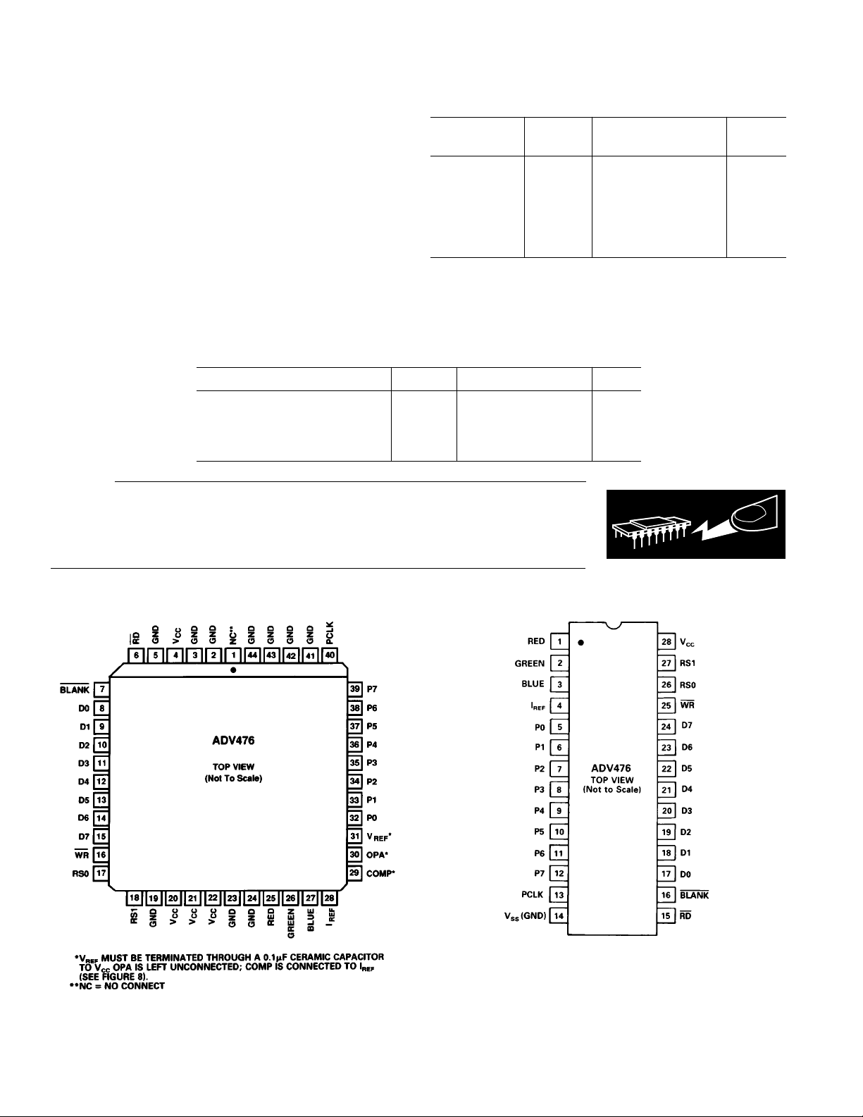
PIN CONFIGURATIONS
The above pins allow the ADV476KP (44-Pin PLCC) to be alternatively driven by a voltage reference. If it is desired to use a
voltage reference configuration instead of the current reference
configuration described in this data sheet, the above listed pins
must be connected as described in Figure 6 of the ADV478/
ADV471 data sheet of this reference manual.
–4–
REV. B
 Loading...