Analog Devices ADV473 Datasheet

CMOS 135 MHz True-Color Graphics
a
FEATURES
ADV478/ADV471 (ADV
IBM PS/2,* VGA*/XGA* Compatible
135 MHz Pipelined Operation
Triple 8-Bit D/A Converters
Triple 256 3 8 (256 3 24) Color Palette RAM
Three 15 3 8 Overlay Registers
On-Board Voltage Reference
RS-343A/RS-170 Compatible Analog Outputs
TTL Compatible Digital Inputs and Outputs
Sync on All Three Channels
Programmable Pedestal (0 or 7.5 IRE)
Standard MPU l/O Interface
+5 V CMOS Monolithic Construction
68-Pin PLCC Package
APPLICATIONS
High Resolution Color Graphics
True-Color Visualization
CAE/CAD/CAM
Image Processing
Desktop Publishing
SYNC
BLANK
S0
S1
RED
GREEN
BLUE
OL0
OL3
R0
R7
G0
G7
B0
B7
OVERLAYS
®
) Register Level Compatible
P
I
4
X
E
L
P
O
8
R
T
8
8
8
8
8
SWITCHING
MATRIX &
PIXEL
MASK
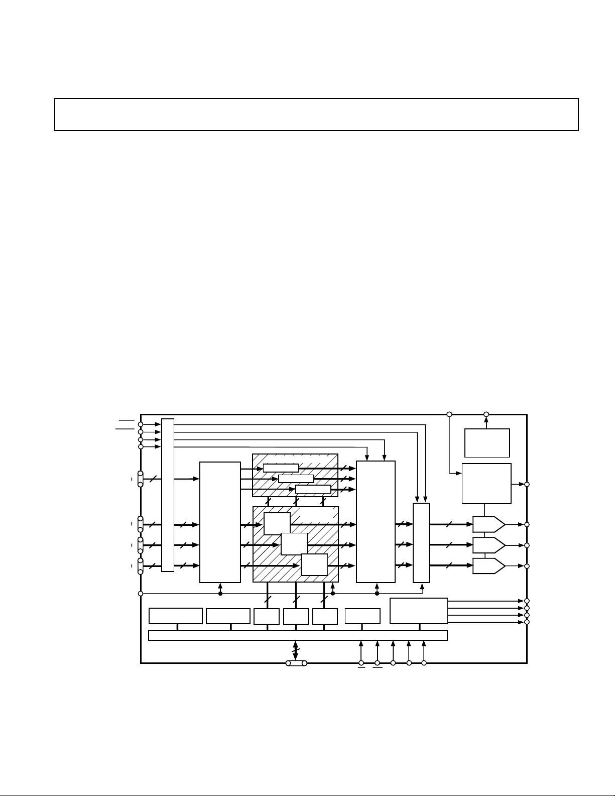
Triple 8-Bit Video RAM-DAC
MODES
24-Bit True Color
8-Bit Pseudo Color
15-Bit True Color
8-Bit True Color
SPEED GRADES
135 MHz, 110 MHz
80 MHz, 66 MHz
GENERAL DESCRIPTION
The ADV473 is a complete analog output, Video RAM-DAC
on a single CMOS monolithic chip. The part is specifically
designed for true-color computer graphics systems.
The ADV473 integrates a number of graphic functions onto one
device allowing 24-bit direct true-color operation at the maximum screen update rate of 135 MHz. It can also be used in
other modes, including 15-bit true color and 8-bit pseudo or indexed color. The ADV473 is fully PS/2 and VGA register level
compatible. It is also capable of implementing IBM’s XGA
standard.
FUNCTIONAL BLOCK DIAGRAM
15 x 8 RAM
8
8
8
OVERLAY PALETTE
15 x 8 RAM
15 x 8 RAM
8 88
GREEN
256 x 8
RAM
COLOR
PALETTE
BLUE
256 x 8
RAM
RED
256 x 8
RAM
8
8
8
8
8
8
COLOR
PALETTE/
OVERLAY
PALETTE
SWITCHER
ADV473
(Continued on page 4)
V
REFIN
D
8
A
C
8
P
O
8
R
T
8
8
8
V
REFOUT
VOLTAGE
REFERENCE
GENERATOR
VOLTAGE
REFERENCE
CONTROL
CIRCUIT
RED
DAC
GREEN
DAC
BLUE
DAC
OPA
IOR
IOG
IOB
CLOCK
MODE CONTROL
REGISTERS
PIXEL MASK
REGISTERS
8 88
RED
REG
GREEN
REG
MPU PORT
8
D0–D7
BLUE
REG
ADDRESS
REG
WR
ADV is a registered trademark of Analog Devices Inc.
*Personal System/2 and VGA are trademarks of International Business Machines Corp.
REV. A
Information furnished by Analog Devices is believed to be accurate and
reliable. However, no responsibility is assumed by Analog Devices for its
use, nor for any infringements of patents or other rights of third parties
which may result from its use. No license is granted by implication or
otherwise under any patent or patent rights of Analog Devices.
One Technology Way, P.O. Box 9106, Norwood, MA 02062-9106, U.S.A.
Tel: 617/329-4700 Fax: 617/326-8703
MPU & PIXEL
PORT
CONTROL LOGIC
RS1 RS2RD
RS0
ADV473
CR0
CR1
CR2
CR3

1
(V
ADV473–SPECIFICA TIONS
= 5 V; V
AA
All specifications T
= 1.235 V; RL = 37.5 Ω, CL = 10 pF; R
REF
MIN
2
to T
unless otherwise noted.)
MAX
= 140 Ω.
SET
Parameter All Versions Units Test Conditions/Comments
STATIC PERFORMANCE
Resolution (Each DAC) 8 Bits
Accuracy (Each DAC)
Integral Nonlinearity ±1 LSB max
Differential Nonlinearity ±1 LSB max Guaranteed Monotonic
Gray Scale Error ±5 % Gray Scale External Reference
±10 % Gray Scale Internal Reference
Coding Binary
DIGITAL INPUTS
Input High Voltage, V
Input Low Voltage, V
Input Current, I
Input Capacitance, C
IN
IN
INH
INL
2 V min
0.8 V max
±1 µA max VIN = 0.4 V or 2.4 V
7 pF max f = 1 MHz, VIN = 2.4 V
DIGITAL OUTPUTS
Output High Voltage, V
Output Low Voltage, V
OL
OH
2.4 V min I
0.4 V max I
SOURCE
= 3.2 mA
SINK
= 400 µA
Floating-State Leakage Current 50 µA max
Floating-State Leakage Capacitance 7 pF max
ANALOG OUTPUTS
Gray Scale Current Range 20 mA max
Output Current
White Level Relative to Black 16.74 mA min Typically 17.62 mA
18.50 mA max
Black Level Relative to Blank 0.95 mA min Typically 1.44 mA
(Pedestal = 7.5 IRE) 1.90 mA max
Black Level Relative to Blank 0 µA min Typically 5 µA
(Pedestal = 0 IRE) 50 µA max
Blank Level 6.29 mA min Typically 7.62 mA
8.96 mA max
Sync Level 0 µA min Typically 5 µA
50 µA max
LSB Size 69.1 µA typ
DAC-to-DAC Matching 2 % max Typically 1%
Output Compliance, V
OC
0 V min
+1.5 V max
Output Capacitance, C
Output Impedance, R
OUT
OUT
30 pF max f = 1 MHz, I
10 kΩ typ
OUT
= 0 mA
VOLTAGE REFERENCE
Internal Voltage Reference (V
) 1.08/1.32 V min/V max Typically 1.235 V
REFOUT
External Voltage Reference Range 1.14/1.26 V min/V max Typically 1.235 V
Input Current, I
(Internal Reference) 100 µA typ
VREF
Input Current (External Reference) 10 µA typ
POWER SUPPLY
Supply Voltage, V
Supply Current, I
AA
AA
3
4.75/5.25 V min/V max
400 mA max 135 MHz Parts
300 mA max 110 MHz Parts
250 mA max 80 MHz Parts
200 mA max 66 MHz Parts
DYNAMIC PERFORMANCE
Clock and Data Feedthrough
Glitch Impulse
4, 5
DAC-to-DAC Crosstalk
NOTES
1
VAA = 5 V ± 5%
2
Temperature range (T
3
Pixel Port is continuously clocked with data corresponding to a linear ramp.
4
Clock and data feedthrough is a function of the amount of overshoot and undershoot on the digital inputs. Glitch impulse includes clock and data feedthrough.
5
TTL input values are 0 to 3 volts, with input rise/fall times ≤ 3 ns, measured at the 10% and 90% points. Timing reference points at 50% for inputs and outputs.
6
DAC to DAC Crosstalk is measured by holding one DAC high while the other two are making low to high and high to low transitions.
Specifications subject to change without notice.
MIN
4, 5
6
to T
); 0°C to +70°C; TJ (Silicon Junction Temperature) ≤ 100°C.
MAX
–30 dB typ
75 pV secs typ
–23 dB typ
–2–
REV. A

ADV473
DATA
IOR, IOG, IOB
NOTES
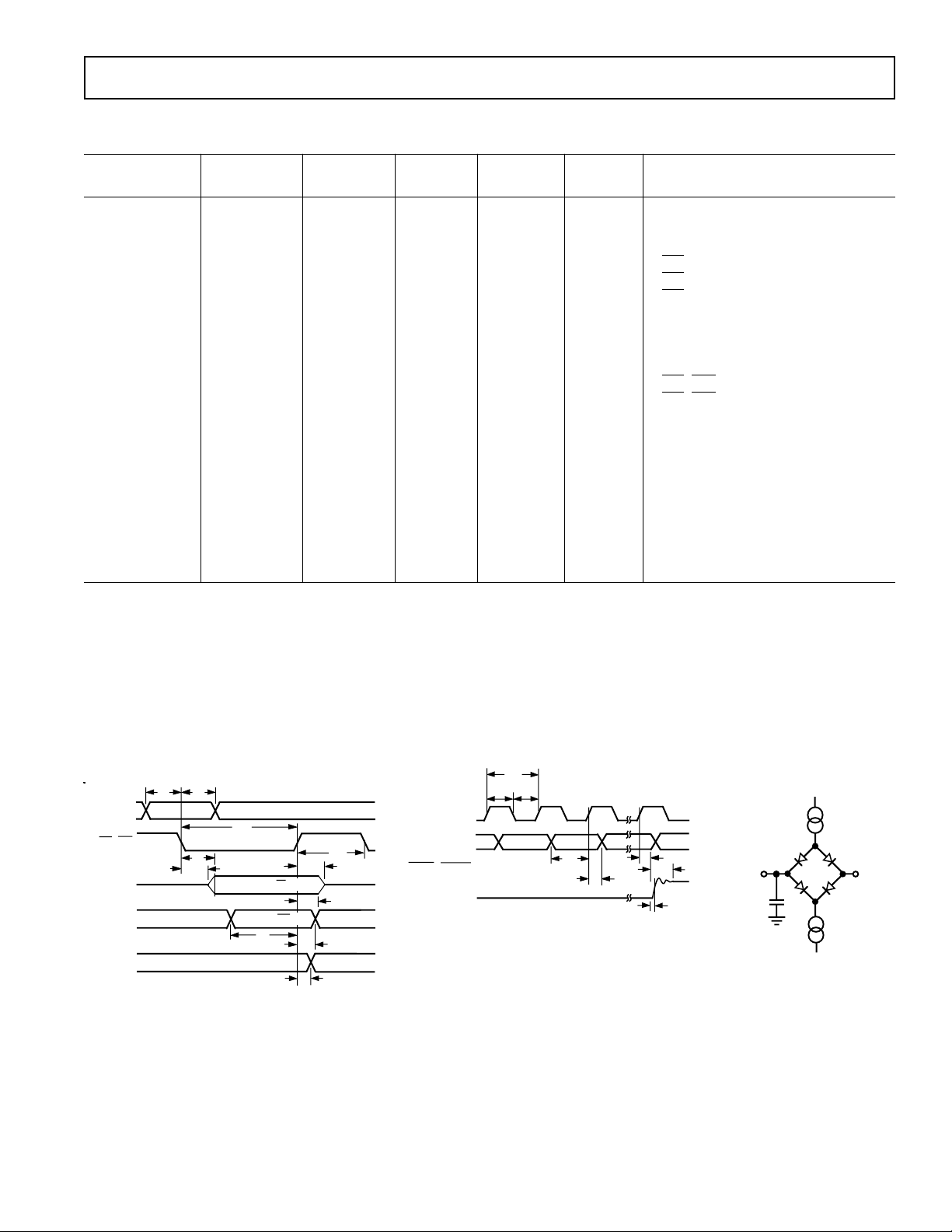
1. OUTPUT DELAY MEASURED FROM THE 50% POINT OF THE RISING EDGE
OF CLOCK TO THE 50% POINT OF FULL-SCALE TRANSITION.
2. SETTLING TIME MEASURED FROM THE 50% POINT OF FULL-SCALE
TRANSITION TO THE OUTPUT REMAINING WITHIN ±1 LSB.
3. OUTPUT RISE/FALL TIME MEASURED BETWEEN THE 10% AND 90%
POINTS OF FULL-SCALE TRANSITION.
CLOCK
R0-R7, G0–G7,
B0–B7,
OL0-OL3, S0–S1,
SYNC, BLANK
t
14
t
16
t
15
t
12
t
19
t
18
t
13
t
17
3.2mA
+2.1V
TO
OUTPUT
PIN
50pF
400µA
2
(V
= 5 V; V
AA
1
TIMING CHARACTERISTICS
All specifications T
135 MHz 110 MHz 80 MHz 66 MHz
Parameter Version Version Version Version Units Conditions/Comments
fmax 135 110 80 66 MHz Clock Rate
t
1
t
2
4
t
3
4
t
4
5
t
5
5
t
6
t
7
t
8
t
9
t
10
t
11
t
12
t
13
t
14
t
15
t
16
t
17
t
18
6
t
19
t
SK
t
PD
NOTES
1
TTL input values are 0 to 3 volts, with input rise/fall times ≤ 3 ns, measured between the 10% and 90% points. Timing reference points at 50% for inputs and
outputs. Analog output load ≤ 10 pF, D0-D7 output load ≤ 50 pF. See timing notes in Figure 2.
2
VAA = 5 V ± 5%.
3
Temperature range (T
4
t3 and t4 are measured with the load circuit of Figure 3 and defined as the time required for an output to cross 0.4 V or 2.4 V.
5
t5 and t6 are derived from the measured time taken by the data outputs to change by 0.5 V when loaded with the circuit of Figure 3. The measured number is
then extrapolated back to remove the effects of charging the 50 pF capacitor. This means that the times, t
true values for the device and, as such, are independent of external bus loading capacitances.
6
Settling time does not include clock and data feedthrough.
Specifications subject to change without notice.
10 10 10 10 ns min RS0–RS2 Setup Time
10 10 10 10 ns min RS0–RS2 Hold Time
3 3 3 3 ns min RD Asserted to Data Bus Driven
40 40 40 40 ns max RD Asserted to Data Valid
20 20 20 20 ns max RD Negated to Data Bus 3-Stated
5 5 5 5 ns min Read Data Hold Time
10 10 10 10 ns min Write Data Setup Time
10 10 10 10 ns min Write Data Hold Time
100 100 100 100 ns max CR0–CR3 Delay Time
50 50 50 50 ns min RD, WR Pulse Width Low
40 40 40 40 ns min RD, WR Pulse Width High
2 3 3 3 ns min Pixel & Control Setup Time
2 3 3 3 ns min Pixel & Control Hold Time
7.4 9.1 12.5 15.15 ns min Clock Cycle Time
3 3.5 4 5 ns min Clock Pulse Width High Time
2 3 4 5 ns min Clock Pulse Width Low Time
30 30 30 30 ns max Analog Output Delay
3 3 3 3 ns typ Analog Output Rise/Fall Time
13 13 13 13 ns max Analog Output Settling Time
2 2 2 2 ns max Analog Output Skew
MIN
4 × t
14
to T
); 0°C to +70°C; TJ (Silicon Junction Temperature) ≤ 100°C .
MAX
4 × t
14
= 1.235 V; RL = 37.5 Ω, CL = 10 pF; R
REF
4 × t
MIN
14
3
to T
unless otherwise noted.)
MAX
4 × t
14
ns Pipeline Delay
= 140 Ω.
SET
and t6, quoted in the timing characteristics are the
5
t
t
1
RS0, RS1,
RS2
RD, WR
D0–D7
(READ)
D0–D7
(WRITE)
CR0–CR3
Figure 1. MPU Read/Write Timing
REV. A
VALID
2
t
4
t
3
t
10
DATA OUT (RD = 0)
DATA IN (WR = 0)
t
7
t
11
t
5
t
6
t
8
t
9
Figure 2. Video Input/Output Timing
Figure 3. Load Circuit for Bus
Access and Relinquish Time
–3–

ADV473
98
7654321686766656463
62 61
27 28
29 30 31 32 33 34 35 36 37 38 39 40 41 42 43
10
11
12
13
14
15
16
17
18
19
20
21
22
23
24
25
26
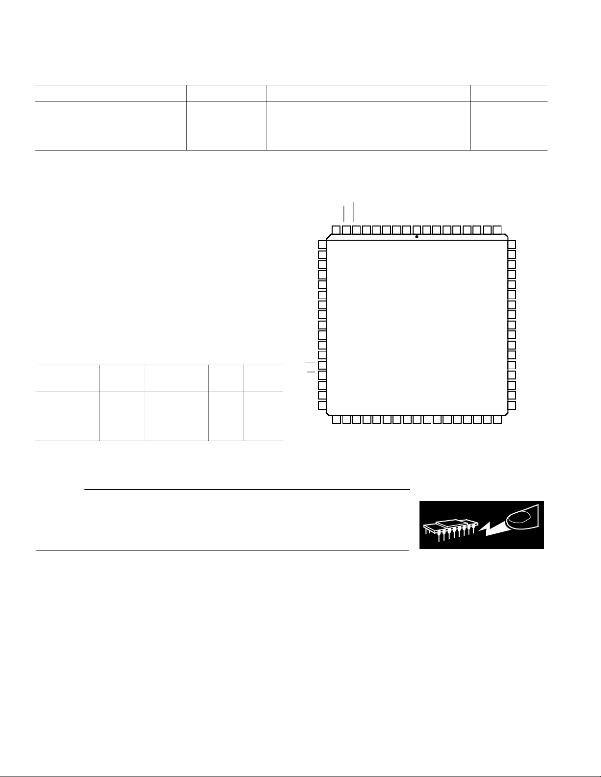
TOP VIEW
(Not To Scale)
ADV473
OL0
OL1
OL2
OL3
D0
D1
D2
D3
D4
D5
D6
D7
RS0
RS1
RS2
WR
RD
CR1
GND
GND
IOG
CR0
CR2
CR3
IOR
IOB
COMP
R
SET
V
REFIN
COMP
V
AA
V
AA
V
AA
V
AA
CLOCK
BLANK
SI
S0
GND
GND
B7
B6
B5
B4
B3
B2
B1
B0
SYNC
V
AA
V
AA
G7
G6
G5
G4
G3
G2
G1
G0
R7
R6
R5
R4
R3
R2
R1
R0
V
REFOUT
59
58
57
56
55
54
53
52
51
50
49
48
47
46
45
44
60
RECOMMENDED OPERATING CONDITIONS
Parameter Symbol Min Typ Max Units
Power Supply V
Ambient Operating Temperature T
Output Load R
Reference Voltage V
ABSOLUTE MAXIMUM RATINGS
1
AA
A
L
REF
4.75 5.00 5.25 Volts
0 +70 °C
1.14 1.235 1.26 Volts
VAA to GND . . . . . . . . . . . . . . . . . . . . . . . . . . . . . . . . . . . 7 V
Voltage on Any Digital Pin . . . . GND – 0.5 V to V
Ambient Operating Temperature (T
Storage Temperature (T
Junction Temperature (T
) . . . . . . . . . . . . . . –65°C to +150°C
S
) . . . . . . . . . . . . . . . . . . . . +150°C
J
) . . . . . –55°C to +125°C
A
+ 0.5 V
AA
Lead Temperature (Soldering, 10 secs) . . . . . . . . . . . +300°C
Vapor Phase Soldering (2 minutes) . . . . . . . . . . . . . . +220°C
IOR, IOG, IOB to GND
NOTES
1
Stresses above those listed under “Absolute Maximum Ratings” may cause
permanent damage to the device. This is a stress rating only and functional
operation of the device at these or any other conditions above those listed in the
operational sections of this specification is not implied. Exposure to absolute
maximum rating conditions for extended periods may affect device reliability.
2
Analog output short circuit to any power supply or common can be of an indefinite
duration.
2
. . . . . . . . . . . . .GND–0.5 V to V
AA
ORDERING GUIDE
Temperature No. of Package
Model Speed Range Pins Option*
37.5 Ω
PIN CONFIGURATION
68-Pin PLCC
ADV473KP135 135 MHz 0°C to +70°C 68 P-68A
ADV473KP110 110 MHz 0°C to +70°C 68 P-68A
ADV473KP80 80 MHz 0°C to +70°C 68 P-68A
ADV473KP66 66 MHz 0°C to +70°C 68 P-68A
NOTE
*
All devices are packaged in a 68-pin plastic leaded (J-lead) chip carrier.
CAUTION
ESD (electrostatic discharge) sensitive device. Electrostatic charges as high as 4000 V readily
accumulate on the human body and test equipment and can discharge without detection.
Although the ADV473 features proprietary ESD protection circuitry, permanent damage may
WARNING!
occur on devices subjected to high energy electrostatic discharges. Therefore, proper ESD
precautions are recommended to avoid performance degradation or loss of functionality.
(Continued from page 1)
The device consists of three, high speed, 8-bit, video D/A converters (RGB), a 256 3 24 RAM which can be configured as a
look-up table or a linearization RAM, a 24-bit wide parallel
pixel input port and three 15 3 8 overlay registers. The part is
controlled through the MPU port by the various on-board control/command registers.
The individual red, green and blue pixel input ports allow truecolor, image rendition. True-color image rendition, at speeds of
up to 135 MHz, is achieved through the 24-bit pixel input port.
The ADV473 is also capable of implementing 8-bit true color,
8-bit pseudo color and 15-bit true color.
The ADV473 is capable of generating RGB video output signals, without requiring external buffering, and which are compatible with RS-343A and RS-170 video standards. All digital
inputs and outputs are TTL compatible.
The part can be driven by the on-board voltage reference or an
external voltage reference.
The part is packaged in a 68-pin Plastic Leaded Chip Carrier
(PLCC).
–4–
ESD SENSITIVE DEVICE
REV. A
 Loading...