

300 MHz, 32 × 16 Buffered
V
V
FEATURES
Large, 32 × 16, nonblocking switch array
G = +1 (ADV3202) or G = +2 (ADV3203) operation
32 × 32 pin-compatible version available (ADV3200/ADV3201)
Single +5 V, dual ±2.5 V, or dual ±3.3 V supply (G = +2)
Serial programming of switch array
2:1 OSD insertion mux per output
Input sync-tip clamp
High impedance output disable allows connection of
multiple devices with minimal output bus load
Excellent video performance
60 MHz 0.1 dB gain flatness
0.1% differential gain error (R
0.1° differential phase error (R
Excellent ac performance
Bandwidth: >300 MHz
Slew rate: >400 V/μs
Low power: 1 W
Low all hostile crosstalk: −48 dB @ 5 MHz
Reset pin allows disabling of all outputs
Connected through a capacitor to ground, provides
power-on reset capability
176-lead exposed pad LQFP package (24 mm × 24 mm)
APPLICATIONS
CCTV sur veillance
Routing of high speed signals, including
Composite video (NTSC, PAL, S, SECAM)
RGB and component video routing
Compressed video (MPEG, wavelet)
Video conferencing
= 150 Ω)
L
= 150 Ω)
L
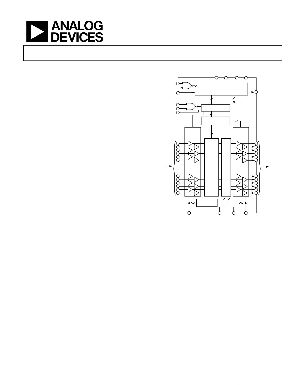
DATA IN
UPDATE
RESET
INPUTS
Analog Crosspoint Switch
ADV3202/ADV3203
FUNCTIONAL BLOCK DIAGRAM
NEG DGNDDVCCPOS
CLK
193-BIT SHI FT REGISTER
OSD
MUX
SWITCHES
96
ADV3202
(ADV3203)
16
ENABLE/
DISABLE
OUTPUT
BUFFER
G = +1
(G = +2)
.
.
.
1616
OSD
.
.
.
CS
ENABLE/
BYPASS
SYNC-TIP
CLAMP
.
.
32
.
VCLAMP VREFOSD
PARALLEL L ATCH
.
.
.
REFERENCE
97
96
16 × 5:32
DECODERS
512
SWITCH
MATRIX
INPUTS
Figure 1.
DATA
OUT
16
OUTPUTS
07526-001
GENERAL DESCRIPTION
The ADV3202/ADV3203 are 32 × 16 analog crosspoint switch
matrices. They feature a selectable sync-tip clamp input for
ac-coupled applications and a 2:1 on-screen display (OSD)
insertion mux. With −48 dB of crosstalk and −80 dB isolation
at 5 MHz, the ADV3202/ADV3203 are useful in many high
density routing applications. The 0.1 dB flatness out to 60 MHz
makes the ADV3202/ADV3203 ideal for both composite and
component video switching.
The 16 independent output buffers of the ADV3202/ADV3203
can be placed into a high impedance state for paralleling crosspoint outputs so that off-channels present minimal loading to
Rev. 0
Information furnished by Analog Devices is believed to be accurate and reliable. However, no
responsibility is assumed by Analog Devices for its use, nor for any infringements of patents or other
rights of third parties that may result from its use. Specifications subject to change without notice. No
license is granted by implication or otherwise under any patent or patent rights of Analog Devices.
Trademarks and registered trademarks are the property of their respective owners.
an output bus if building a larger array. The ADV3202 has a
gain of +1 while the ADV3203 has a gain of +2 for ease of use in
back-terminated load applications. A single +5 V supply, dual
±2.5 V supplies, or dual ±3.3 V supplies (G = +2) can be used
while consuming only 195 mA of idle current with all outputs
enabled. The channel switching is performed via a double
buffered, serial digital control that can accommodate daisy
chaining of several devices.
The ADV3202/ADV3203 are packaged in a 176-lead exposed
pad LQFP package (24 mm× 24 mm) and are available over the
extended industrial temperature range of −40°C to +85°C.
One Technology Way, P.O. Box 9106, Norwood, MA 02062-9106, U.S.A.
Tel: 781.329.4700 www.analog.com
Fax: 781.461.3113 ©2008 Analog Devices, Inc. All rights reserved.

ADV3202/ADV3203
TABLE OF CONTENTS
Features .............................................................................................. 1
Applications ....................................................................................... 1
Functional Block Diagram .............................................................. 1
General Description ......................................................................... 1
Revision History ............................................................................... 2
Specifications ..................................................................................... 3
OSD Disabled ................................................................................ 3
OSD Enabled ................................................................................. 4
Timing Characteristics (Serial Mode) ....................................... 5
Absolute Maximum Ratings ............................................................ 6
Thermal Resistance ...................................................................... 6
REVISION HISTORY
10/08—Revision 0: Initial Version
Power Dissipation..........................................................................6
ESD Caution...................................................................................6
Pin Configuration and Function Descriptions ..............................7
Truth Table and Logic Diagram ............................................... 10
Typical Performance Characteristics ........................................... 11
Theory of Operation ...................................................................... 14
Applications Information .............................................................. 16
Programming .............................................................................. 16
Outline Dimensions ....................................................................... 17
Ordering Guide .......................................................................... 17
Rev. 0 | Page 2 of 20

ADV3202/ADV3203
SPECIFICATIONS
OSD DISABLED
VS = ±2.5 V (ADV3202), VS = ±3.3 V (ADV3203) at TA = 25°C, G = +1 (ADV3202), G = +2 (ADV3203), RL = 150 Ω, all configurations,
unless otherwise noted.
Table 1.
ADV3202/ADV3203
Parameter Conditions
DYNAMIC PERFORMANCE
−3 dB Bandwidth 200 mV p-p
2 V p-p 120 MHz
Gain Flatness 0.1 dB, 200 mV p-p 60 MHz
0.1 dB, 2 V p-p 40 MHz
Settling Time 1% , 2 V step 6 ns
Slew Rate 2 V step, peak 400 V/μs
NOISE/DISTORTION PERFORMANCE
Differential Gain Error NTSC or PAL 0.06/0.1 %
Differential Phase Error NTSC or PAL 0.06/0.03 Degrees
Crosstalk, All Hostile, RTI f = 5 MHz, RL = 150 Ω
= 1 kΩ
R
L
f = 100 MHz, RL = 150 Ω
= 1 kΩ
R
L
Off Isolation, Input-to-Output f = 5 MHz, one channel −80 dB
Input Voltage Noise 0.1 MHz to 50 MHz 25/22 nV/√Hz
DC PERFORMANCE
Gain Error Broadcast mode, no load ±0.5 ±1.75/±2.2 %
Broadcast mode ±0.5 ±2.2/±2.7 %
Gain Matching No load, channel-to-channel ±0.5/±0.8 ±2.8 %
Channel-to-channel ±0.5/±0.8 ±3.4 %
OUTPUT CHARACTERISTICS
Output Impedance DC, enabled 0.15 Ω
DC, disabled 900/3.2 1000/4 kΩ
Output Capacitance Disabled 3.7 pF
Output Voltage Range ADV3202
ADV3203
ADV3203, no output load
INPUT CHARACTERISTICS
Input Offset Voltage ±5 ±30 mV
Input Voltage Range ADV3202
ADV3203
ADV3203, no output load
Input Capacitance 3 pF
Input Resistance 1 4 MΩ
Input Bias Current
Sync-tip clamp disabled −10 −3 μA
SWITCHING CHARACTERISTICS
Enable On Time 50% update to 1% settling 50 ns
Switching Time, 2 V Step 50% update to 1% settling 40 ns
Switching Transient (Glitch) IN00 to IN31, RTI 300 mV p-p
Sync-tip clamp enabled,
= VCLAMP + 0.1 V
V
IN
Sync-tip clamp enabled,
= VCLAMP − 0.1 V
V
IN
−48
−23
−1.1 to +1.1
−1.5 to +1.5
−1.5 to +1.5
−1.1 to +1.1
−0.75 to +0.75
−0.75 to +0.75
0.1 3 12 μA
−2.9 −1 −0.25 mA
300 MHz
dB
−65
dB
−30
−1.2 to +1.2
−1.6 to +2.0
−2.0 to +2.0
−1.2 to +1.2
−0.8 to +1.0
−1.0 to +1.0
V
V
Unit Min Typ Max
dB
dB
V
V
V
V
Rev. 0 | Page 3 of 20

ADV3202/ADV3203
ADV3202/ADV3203
Parameter Conditions
POWER SUPPLIES
Supply Current
or V
V
POS
, outputs enabled,
NEG
195/200 220/235 mA
no load
V
D
Supply Voltage Range V
or V
POS
VCC
POS
, outputs disabled 120/130 155/165 mA
NEG
2.5 3.5 mA
− V
NEG
5 ± 10%/
V
6.6 ± 10%
PSR V
, V
, f = 1 MHz −50/−45 dB
NEG
POS
OPERATING TEMPERATURE RANGE
Temperature Range Operating (still air) −40 to +85 °C
θJA Operating (still air) 16 °C/W
OSD ENABLED
VS = ±2.5 V (ADV3202), VS = ±3.3 V (ADV3203) at TA = 25°C, G = +1 (ADV3202), G = +2 (ADV3203), RL = 150 Ω, all configurations,
unless otherwise noted.
Table 2.
ADV3202/ADV3203
Parameter Conditions
OSD DYNAMIC PERFORMANCE
−3 dB Bandwidth 200 mV p-p
2 V p-p 135/130 MHz
Gain Flatness 0.1 dB, 200 mV p-p 35 MHz
0.1 dB, 2 V p-p 35 MHz
Settling Time 1%, 2 V step 6 ns
Slew Rate 2 V step, peak 400 V/μs
OSD NOISE/DISTORTION PERFORMANCE
Differential Gain Error NTSC or PAL 0.12/0.35 %
Differential Phase Error NTSC or PAL 0.06/0.04 Degrees
Input Voltage Noise 0.5 MHz to 50 MHz 27/25 nV/√Hz
OSD DC PERFORMANCE
Gain Error No load ±0.1 ±2.3/±2.2 %
±0.1 ±2.7 %
OSD INPUT CHARACTERISTICS
Input Bias Current Sync-tip clamp disabled −10 −4 μA
OSD SWITCHING CHARACTERISTICS
OSD Switch Delay, 2 V Step 50% OSD switch to 1% settling 20 ns
OSD Switching Transient (Glitch) 15/40 mV p-p
170/150 MHz
Unit Min Typ Max
Unit Min Typ Max
Rev. 0 | Page 4 of 20
ADV3202/ADV3203
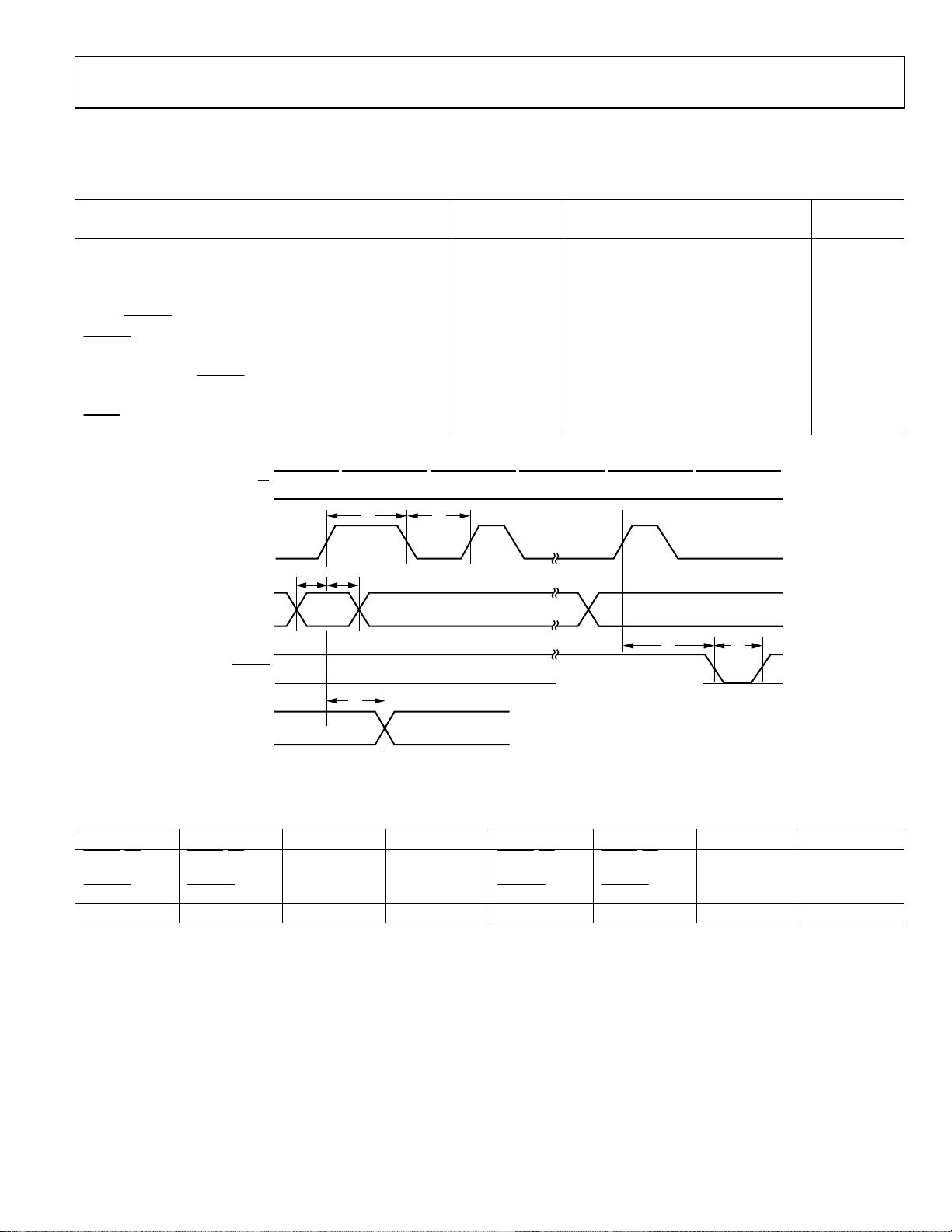
TIMING CHARACTERISTICS (SERIAL MODE)
Specifications subject to change without notice.
Table 3.
Limit
Parameter Symbol Min Typ Max Unit
Serial Data Setup Time t1 40 ns
CLK Pulse Width t2 50 ns
Serial Data Hold Time t3 50 ns
CLK Pulse Separation t4 150 ns
t
CLK to UPDATE Delay
UPDATE Pulse Width
CLK to DATA OUT Valid t7 130 ns
Propagation Delay, UPDATE to Switch On or Off
Data Load Time, CLK = 5 MHz, Serial Mode 38.6 μs
RESET Time
1
CS
0
t
2
3
t
7
CLK
DATA IN
1 = LATCHED
UPDATE
0 = TRANSPARENT
DATA OUT
1
0
t1t
1
0
CLAMP
ON/OFF
Figure 2. Timing Diagram, Serial Mode
50 160 ns
5
t
40 ns
6
50 ns
160 ns
t
4
LOAD DATA INT O
SERIAL REGI STER
ON RISING E DGE
TRANSFER DATA FRO M SERIAL
REGISTER TO PARALLEL
LATCHES DURING LOW LE VEL
OUT00 (D0)OUT15 (D5)
t
5
t
6
7526-002
Table 4. Logic Levels, DVCC = 3.3 V
VIH VIL V
RESET, CS,
CLK, DATA IN,
UPDATE
, OSDS
RESET
, CS,
CLK, DATA IN,
UPDATE
, OSDS
V
OH
I
OL
DATA OUT DATA OUT
I
IH
, CS,
RESET
CLK, DATA IN,
UPDATE
, OSDS
I
IL
RESET
, CS,
CLK, DATA IN,
UPDATE
, OSDS
I
OH
OL
DATA OUT DATA OUT
2.5 V min 0.8 V max 2.7 V min 0.5 V max 0.5 μA typ −0.5 μA typ 3 mA typ −3 mA typ
Rev. 0 | Page 5 of 20
ADV3202/ADV3203
ABSOLUTE MAXIMUM RATINGS
Table 5.
Parameter Rating
Analog Supply Voltage (V
Digital Supply Voltage
(DVCC − D
GND
)
Ground Potential Difference
(V
− D
GND
)
NEG
Maximum Potential Difference
DVCC − V
9.4 V
NEG
Disabled Outputs
ADV3202 (|V
ADV3203 (|V
|V
− V
CLAMP
V
Input Voltage
REF
OSD
OSD
| 6 V
INxx
ADV3202 V
ADV3203 V
Analog Input Voltage V
Digital Input Voltage DVCC
Output Voltage
(Disabled Analog Output)
Output Short-Circuit Duration Momentary
Output Short-Circuit Current 45 mA
Storage Temperature Range −65°C to +125°C
Operating Temperature Range −40°C to +85°C
Lead Temperature
(Soldering, 10 sec)
Junction Temperature 150°C
− V
POS
) 7.5 V
NEG
6 V
+0.5 V to –4 V
− V
|) <3 V
OUT
−(V
OUT+VREF
)/2|) <3 V
(V
300°C
– 3.5 V to V
POS
– 4 V to V
POS
to V
NEG
− 1 V) to (V
POS
POS
+ 3.5 V
NEG
+ 4 V
NEG
+ 1 V)
NEG
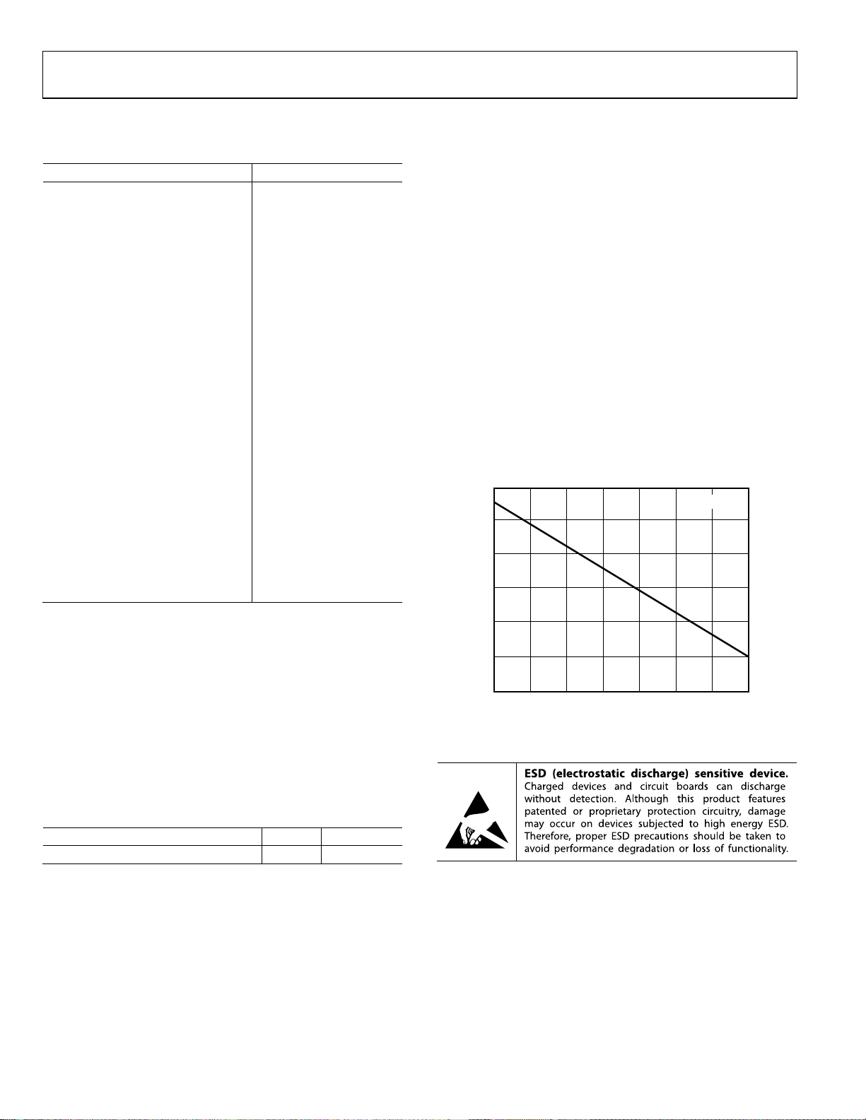
POWER DISSIPATION
The ADV3202/ADV3203 are operated with ±2.5 V, +5 V, or
±3.3 V supplies and can drive loads down to 150 , resulting in
a large range of possible power dissipations. For this reason,
extra care must be taken while derating the operating conditions
based on ambient temperature.
Packaged in a 176-lead exposed-pad LQFP, the ADV3202/
ADV3203 junction-to-ambient thermal impedance (θ
16°C/W. For long-term reliability, the maximum allowed
junction temperature of the die should not exceed 150°C.
Temporarily exceeding this limit may cause a shift in parametric
performance due to a change in stresses exerted on the die by
the package. Exceeding a junction temperature of 175°C for an
extended period can result in device failure. Figure 3 shows the
range of allowed internal die power dissipations that meet these
conditions over the −40°C to +85°C ambient temperature range.
When using Figure 3, do not include external load power in the
maximum power calculation, but do include load current
dropped on the die output transistors.
9
TJ = 150°C
8
7
6
JA
) is
Stresses above those listed under Absolute Maximum Ratings
may cause permanent damage to the device. This is a stress
rating only; functional operation of the device at these or any
other conditions above those indicated in the operational
section of this specification is not implied. Exposure to absolute
maximum rating conditions for extended periods may affect
device reliability.
THERMAL RESISTANCE
θJA is specified for the worst-case conditions, that is, a device
soldered in a circuit board for surface-mount packages.
Table 6. Thermal Resistance
Package Type θJA Unit
176-Lead LQFP_EP 16 °C/W
5
MAXIMUM POWER (W)
4
3
15 25 35 45 55 65 75 85
Figure 3. Maximum Die Power Dissipation vs. Ambient Temperature
AMBIENT TEM PERATURE (°C)
ESD CAUTION
07526-003
Rev. 0 | Page 6 of 20

ADV3202/ADV3203
PIN CONFIGURATION AND FUNCTION DESCRIPTIONS
NC
NC
VPOS
VNEG
NC
VPOS
VNEG
VPOS
VNEG
NC
VPOS
NC
VNEG
VPOS
NC
VNEG
VPOS
VNEG
VPOS
VNEG
VPOS
VNEG
NC
VPOS
148
150
151NC152
153
155NC156
168
165NC166
167
169NC170NC171NC172
161NC162
163NC164
157NC158
159NC160
154
ADV3202/ADV3203
TOP VIEW
(Not to Scale)
147
149
143NC144
145NC146
139
133
135NC136
132
VNEG
131
NC
130
NC
129
NC
128
NC
127
NC
126
OSDS00
125
IN16
124
OSDS01
123
IN17
122
OSDS02
121
IN18
120
OSDS03
119
IN19
118
OSDS04
117
IN20
116
OSDS05
115
IN21
114
OSDS06
113
IN22
112
OSDS07
111
IN23
110
OSDS08
109
IN24
108
OSDS09
107
IN25
106
OSDS10
105
IN26
104
OSDS11
103
IN27
102
OSDS12
101
IN28
100
OSDS13
99
IN29
98
OSDS14
97
IN30
96
OSDS15
95
IN31
94
VPOS
93
OSD00
92
OSD01
91
OSD02
90
OSD03
89
VNEG
134
137NC138
140
141NC142
DVCC
NC
RESET
CLK
DATA IN
DATA OUT
UPDATE
CS
DGND
IN00
DGND
IN01
DGND
IN02
DGND
IN03
DGND
IN04
DGND
IN05
DGND
IN06
DGND
IN07
DGND
IN08
DGND
IN09
DGND
IN10
DGND
IN11
DGND
IN12
DGND
IN13
DGND
IN14
DGND
IN15
VNEG
VREF
VCLAMP
OSD15
NC
NC
DGND
173
174NC175NC176
1
PIN 1
2
3
4
5
6
7
8
9
10
11
12
13
14
15
16
17
18
19
20
21
22
23
24
25
26
27
28
29
30
31
32
33
34
35
36
37
38
39
40
41
42
43
44
45
48
49
52
53
OSD1050OSD0951OSD08
VPOS
OUT15
OSD11
NOTES
1. NC = NO CONNECT
2. OSDS#: OSD SELECT F OR OUTPUT #
OSD#: OSD VI DEO INPUT FOR OUTP UT #
3. THE EXPOSED PAD SHOULD BE
CONNECTED TO ANALOG GRO UND.
OSD1446OSD1347OSD12
54
55
56
57
58
59
60
61
62
63
64
65
66
67
68
69
70
71
72
73
74
75
76
77
78
79
80
81
82
83
84
85
VPOS
VNEG
OUT14
VPOS
VNEG
OUT13
OUT12
VPOS
VNEG
OUT11
OUT10
VPOS
VNEG
OUT09
OUT08
VPOS
VNEG
OUT07
OUT06
VPOS
VNEG
OUT05
OUT04
VPOS
VNEG
OUT03
OUT02
VPOS
VNEG
OUT01
OUT00
OSD0786OSD0687OSD0588OSD04
07526-004
Figure 4. Pin Configuration
Rev. 0 | Page 7 of 20

ADV3202/ADV3203
Table 7. Pin Function Descriptions
Pin Mnemonic Description
1 DVCC Digital Positive Power Supply.
2 NC No Connect.
3
RESET
4 CLK Control Pin: Serial Data Clock.
5 DATA IN Control Pin: Serial Data In.
6 DATA OUT Control Pin: Serial Data Out.
7
8
UPDATE
CS
9 DGND Digital Negative Power Supply.
10 IN00 Input Number 0.
11 DGND Digital Negative Power Supply.
12 IN01 Input Number 1.
13 DGND Digital Negative Power Supply.
14 IN02 Input Number 2.
15 DGND Digital Negative Power Supply.
16 IN03 Input Number 3.
17 DGND Digital Negative Power Supply.
18 IN04 Input Number 4.
19 DGND Digital Negative Power Supply.
20 IN05 Input Number 5.
21 DGND Digital Negative Power Supply.
22 IN06 Input Number 6.
23 DGND Digital Negative Power Supply.
24 IN07 Input Number 7.
25 DGND Digital Negative Power Supply.
26 IN08 Input Number 8.
27 DGND Digital Negative Power Supply.
28 IN09 Input Number 9.
29 DGND Digital Negative Power Supply.
30 IN10 Input Number 10.
31 DGND Digital Negative Power Supply.
32 IN11 Input Number 11.
33 DGND Digital Negative Power Supply.
34 IN12 Input Number 12.
35 DGND Digital Negative Power Supply.
36 IN13 Input Number 13.
37 DGND Digital Negative Power Supply.
38 IN14 Input Number 14.
39 DGND Digital Negative Power Supply.
40 IN15 Input Number 15.
41 VNEG Analog Negative Power Supply.
42 VREF
43 VCLAMP
44 OSD15 OSD Input Number 15.
45 OSD14 OSD Input Number 14.
46 OSD13 OSD Input Number 13.
47 OSD12 OSD Input Number 12.
48 OSD11 OSD Input Number 11.
49 OSD10 OSD Input Number 10.
Control Pin: 1st and 2nd Rank Reset.
Control Pin: Second Rank Write Strobe.
Control Pin: Chip Select.
Reference Voltage. See the Theory of
Operation section for details.
Sync-Tip Clamp Voltage. See the
Theory of Operation section for details.
Pin Mnemonic Description
50 OSD09 OSD Input Number 9.
51 OSD08 OSD Input Number 8.
52 VPOS Analog Positive Power Supply.
53 OUT15 Output Number 15.
54 VNEG Analog Negative Power Supply.
55 OUT14 Output Number 14.
56 VPOS Analog Positive Power Supply.
57 OUT13 Output Number 13.
58 VNEG Analog Negative Power Supply.
59 OUT12 Output Number 12.
60 VPOS Analog Positive Power Supply.
61 OUT11 Output Number 11.
62 VNEG Analog Negative Power Supply.
63 OUT10 Output Number 10.
64 VPOS Analog Positive Power Supply.
65 OUT09 Output Number 9.
66 VNEG Analog Negative Power Supply.
67 OUT08 Output Number 8.
68 VPOS Analog Positive Power Supply.
69 OUT07 Output Number 7.
70 VNEG Analog Negative Power Supply.
71 OUT06 Output Number 6.
72 VPOS Analog Positive Power Supply.
73 OUT05 Output Number 5.
74 VNEG Analog Negative Power Supply.
75 OUT04 Output number 4.
76 VPOS Analog Positive Power Supply.
77 OUT03 Output Number 3.
78 VNEG Analog Negative Power Supply.
79 OUT02 Output Number 2.
80 VPOS Analog Positive Power Supply.
81 OUT01 Output Number 1.
82 VNEG Analog Negative Power Supply.
83 OUT00 Output Number 0.
84 VPOS Analog Positive Power Supply.
85 OSD07 OSD Input Number 7.
86 OSD06 OSD Input Number 6.
87 OSD05 OSD Input Number 5.
88 OSD04 OSD Input Number 4.
89 VNEG Analog Negative Power Supply.
90 OSD03 OSD Input Number 3.
91 OSD02 OSD Input Number 2.
92 OSD01 OSD Input Number 1.
93 OSD00 OSD Input Number 0.
94 VPOS Analog Positive Power Supply.
95 IN31 Input Number 31.
96 OSDS15 Control Pin: OSD Select Number 15.
97 IN30 Input Number 30.
98 OSDS14 Control Pin: OSD Select Number 14.
99 IN29 Input Number 29.
100 OSDS13 Control Pin: OSD Select Number 13.
Rev. 0 | Page 8 of 20

ADV3202/ADV3203
Pin Mnemonic Description
101 IN28 Input Number 28.
102 OSDS12 Control Pin: OSD Select Number 12.
103 IN27 Input Number 27.
104 OSDS11 Control Pin: OSD Select Number 11.
105 IN26 Input Number 26.
106 OSDS10 Control Pin: OSD Select Number 10.
107 IN25 Input Number 25.
108 OSDS09 Control Pin: OSD Select Number 9.
109 IN24 Input Number 24.
110 OSDS08 Control Pin: OSD Select Number 8.
111 IN23 Input Number 23.
112 OSDS07 Control Pin: OSD Select Number 7.
113 IN22 Input Number 22.
114 OSDS06 Control Pin: OSD Select Number 6.
115 IN21 Input Number 21.
116 OSDS05 Control Pin: OSD Select Number 5.
117 IN20 Input Number 20.
118 OSDS04 Control Pin: OSD Select Number 4.
119 IN19 Input Number 19.
120 OSDS03 Control Pin: OSD Select Number 3.
121 IN18 Input Number 18.
122 OSDS02 Control Pin: OSD Select Number 2.
123 IN17 Input Number 17.
124 OSDS01 Control Pin: OSD Select Number 1.
125 IN16 Input Number 16.
126 OSDS00 Control Pin: OSD Select Number 0.
127 NC No Connect.
128 NC No Connect.
129 NC No Connect.
130 NC No Connect.
131 NC No Connect.
132 VNEG Analog Negative Power Supply.
133 NC No Connect.
134 NC No Connect.
135 NC No Connect.
136 VPOS Analog Positive Power Supply.
137 NC No Connect.
138 VNEG Analog Negative Power Supply.
139 NC No Connect.
Pin Mnemonic Description
140 VPOS Analog Positive Power Supply.
141 NC No Connect.
142 VNEG Analog Negative Power Supply.
143 NC No Connect.
144 VPOS Analog Positive Power Supply.
145 NC No Connect.
146 VNEG Analog Negative Power Supply.
147 NC No Connect.
148 VPOS Analog Positive Power Supply.
149 NC No Connect.
150 VNEG Analog Negative Power Supply.
151 NC No Connect.
152 VPOS Analog Positive Power Supply.
153 NC No Connect.
154 VNEG Analog Negative Power Supply.
155 NC No Connect.
156 VPOS Analog Positive Power Supply.
157 NC No Connect.
158 VNEG Analog Negative Power Supply.
159 NC No Connect.
160 VPOS Analog Positive Power Supply.
161 NC No Connect.
162 VNEG Analog Negative Power Supply.
163 NC No Connect.
164 VPOS Analog Positive Power Supply.
165 NC No Connect.
166 VNEG Analog Negative Power Supply.
167 NC No Connect.
168 VPOS Analog Positive Power Supply.
169 NC No Connect.
170 NC No Connect.
171 NC No Connect.
172 NC No Connect.
173 NC No Connect.
174 NC No Connect.
175 NC No Connect.
176 DGND Digital Negative Power Supply.
EPAD
(exposed pad)
Connect to analog ground.
Rev. 0 | Page 9 of 20

ADV3202/ADV3203
TRUTH TABLE AND LOGIC DIAGRAM
Table 8. Operation Truth Table
CS UPDATE
CLK DATA INPUT DATA OUTPUT
X X X X X 0
0 1
Data
1
i
Data
1
i-193
0 0 X X X 1
1 X X X X 1 Chip is not selected. No change in logic.
1
Datai: serial data.
RESET
Operation/Comment
Asynchronous reset. All outputs are disabled; the 193-bit shift
register is reset to all 0s.
The data on the serial DATA IN line is loaded into the serial
register. The first bit clocked into the serial register appears at
DATA OUT 193 clock cycles later.
Switch matrix update. Data in the 193-bit shift register transfers
into the parallel latches that control the switch array and synctip clamps.
Rev. 0 | Page 10 of 20

ADV3202/ADV3203
TYPICAL PERFORMANCE CHARACTERISTICS
VS = ±2.5 V (ADV3202), VS = ±3.3 V (ADV3203) at TA = 25°C, RL = 150 .
2
0
INxx
1.2
0.8
–2
–4
–6
GAIN (dB)
–8
–10
–12
1 10 100 1k
FREQUENCY (MHz )
OSDxx
Figure 5. ADV3202 Small Signal Frequency Response, 200 mV p-p
2
0
–2
–4
–6
GAIN (dB)
–8
–10
OSDxx
INxx
0.4
(V)
0
OUT
V
–0.4
–0.8
–1.2
0 2 4 6 8 101214 161820
07526-005
TIME (ns)
OSDxx
INxx
07526-008
Figure 8. ADV3202 Large Signal Pulse Response, 2 V p-p
600
400
200
0
dV/dT (V/µs)
–200
–400
RISING EDG E
FALLING EDGE
–12
1 10 100 1k
FREQUENCY (MHz )
Figure 6. ADV3202 Large Signal Frequency Response, 2 V p-p
0.12
0.08
0.04
(V)
0
OUT
V
–0.04
OSDxx
–0.08
–0.12
0 2 4 6 8 101214 161820
TIME (ns)
INxx
Figure 7. ADV3202 Small Signal Pulse Response, 200 mV p-p
07526-006
07526-007
Rev. 0 | Page 11 of
–600
024 68101214161820
TIME (ns)
Figure 9. ADV3202 Slew Rate
0.05
0.04
0.03
0.02
0.01
0
–0.01
–0.02
DIFFERENTIAL GAIN (%)
–0.03
–0.04
–0.05
–0.7 –0.5 –0.3 –0.1 0.1 0.3 0.5 0.7
INPUT DC OFFSET (V)
Figure 10. ADV3202 Differential Gain, Carrier Frequency = 3.58 MHz,
Subcarrier Amplitude = 300 mV p-p
20
07526-009
07526-010

ADV3202/ADV3203
0.010
0.12
0.005
0
–0.005
–0.010
DIFFERE NTIAL PHASE (Degrees)
–0.015
–0.020
–0.7 –0.5 –0.3 –0.1 0.1 0.3 0.5 0.7
INPUT DC OFFSET (V)
Figure 11. ADV3202 Differential Phase, Carrier Frequency = 3.58 MHz,
Subcarrier Amplitude = 300 mV p-p
8
6
4
2
OSDxx
0
GAIN (dB)
–2
–4
INxx
0.08
0.04
(V)
0
OUT
V
–0.04
OSDxx
–0.08
–0.12
0 2 4 6 8 101214 161820
07526-011
TIME (ns)
INxx
07526-014
Figure 14. ADV3203 Small Signal Pulse Response, 200 mV p-p
1.2
0.8
0.4
(V)
0
OUT
V
–0.4
–0.8
OSDxx
INxx
–6
1 10 100 1k
FREQUENCY (MHz)
Figure 12. ADV3203 Small Signal Frequency Response, 200 mV p-p
8
6
4
2
0
GAIN (dB)
–2
–4
–6
1 10 100 1k
OSDxx
FREQUENCY (MHz)
INxx
Figure 13. ADV3203 Large Signal Frequency Response, 2 V p-p
–1.2
526-01207
0 2 4 6 8 101214 161820
TIME (ns)
07526-015
Figure 15. ADV3203 Large Signal Pulse Response, 2 V p-p
600
400
RISING EDGE
200
0
dV/dT (V/µs)
–200
–400
–600
0 2 4 6 8 101214 161820
07526-013
TIME (ns)
FALLING EDGE
6-016
0752
Figure 16. ADV3203 Slew Rate
Rev. 0 | Page 12 of 20

ADV3202/ADV3203
0.10
0.05
0
–0.05
DIFFERENTIAL GAIN (%)
–0.10
–0.15
–0.7 –0.5 –0.3 –0.1 0.1 0.3 0.5 0.7
INPUT DC OFFSET (V)
Figure 17. ADV3203 Differential Gain, Carrier Frequency = 3.58 MHz,
Subcarrier Amplitude = 300 mV p-p
0.05
0.04
0.03
0.02
0.01
0
–0.01
–0.02
–0.03
DIFFERE NTIAL PHASE (Degrees)
–0.04
–0.05
–0.7 –0.5 –0.3 –0.1 0.1 0.3 0.5 0.7
INPUT DC OFFSET (V)
Figure 18. ADV3203 Differential Phase, Carrier Frequency = 3.58 MHz,
Subcarrier Amplitude = 300 mV p-p
6-017
0752
07526-018
Rev. 0 | Page 13 of 20

ADV3202/ADV3203
V
V
V
V
V
THEORY OF OPERATION
The ADV3202/ADV3203 are single-ended crosspoint arrays
with 16 outputs, each of which can be connected to any one
of 32 inputs.The 32 switchable input stages are connected to
each output buffer to form 32-to-1 multiplexers. There are 16 of
these multiplexers, each with its inputs wired in parallel, for a
total array of 512 stages forming a multicast-capable crosspoint
switch. In addition to connecting to any of the nominal inputs
(INxx), each output can also be connected to an associated OSD
input through an additional 2-to-1 multiplexer at each output.
This 2-to-1 multiplexer switches between the output of the 32to-1 multiplexer and the OSD input.
POS
VNEG
VPOS
VNEG
POS
VNEG
VPOS
VNEG
VPOS
VNEG
OSDS00
OSDS00
OUT00
x1
907526-01
OUT00
x1
2kΩ
2kΩ
2007526-0
FROM INPUT
STAGES
OSD00
Figure 19. Conceptual Diagram of Single Output Channel, G = +1 (ADV3202)
Decoding logic for each output selects one (or none) of the
input stages to drive the output stage. The enabled input stage
drives the output stage, which is configured as a unity-gain
amplifier in the ADV3202 (see Figure 19). In the ADV3203, an
internal resistive feedback network and reference buffer provide
for a total output stage gain of +2 (see Figure 20). The input
voltage to the reference buffer is the VREF pin. This voltage is
common for the entire chip and needs to be driven with a low
impedance to avoid crosstalk.
FROM INPUT
STAGES
OSD00
VREF
Figure 20. Conceptual Diagram of Single Output Channel, G = +2 (ADV3203)
Each input to the ADV3202/ADV3203 is buffered by a receiver.
The purpose of this receiver is to provide overvoltage protection
for the input stages by limiting signal swing. In the ADV3202,
the output of the receiver is limited to ±1.2 V about VREF,
while in the ADV3203, the signal swing is limited to ±1.2 V
about midsupply. This receiver is configured as a voltage
feedback unity-gain amplifier. Excess loop gain bandwidth
product reduces the effect of the closed-loop gain on the
bandwidth of the device. In addition to a receiver, each input
also has a sync-tip clamp for use in ac-coupled applications.
This clamp is either enabled or disabled according to the 193
rd
serial data bit. When enabled, the clamp forces the lowest video
voltage to the voltage on the VCLAMP pin. The VCLAMP pin
is common for the entire chip and needs to be driven with a low
impedance to avoid crosstalk.
POS
CLAMP
IN00
CAPACITOR
Figure 21. Conceptual Diagram of Sync-Tip Clamp in an
VNEG
OFF-CHIP
AC-Coupled Application
5µA
POS
TO INPUT
RECEIVER
07526-021
The output stage of the ADV3202/ADV3203 is designed for low
differential gain and phase error when driving composite video
signals. It also provides slew current for fast pulse response
when driving component video signals.
The outputs of the ADV3202/ADV3203 can be disabled to
minimize on-chip power dissipation. When disabled, a series of
internal amplifiers drive internal nodes such that a wideband
high impedance is presented at the disabled output, even while
the output bus is under large signal swings. (In the ADV3203,
there is 4 k of resistance terminated to the VREF voltage by
the reference buffer). This high impedance allows multiple ICs
to be bussed together without additional buffering. Care must
be taken to reduce output capacitance, which results in more
overshoot and frequency domain peaking. In addition, when
the outputs are disabled and driven externally, the voltage
applied to them should not exceed the valid output swing range
for the ADV3202/ADV3203 to keep these internal amplifiers in
their linear range of operation. Applying excess voltage to the
disabled outputs can cause damage to the ADV3202/ADV3203
and should be avoided (see the Absolute Maximum Ratings
section for guidelines).
Rev. 0 | Page 14 of 20

ADV3202/ADV3203
The internal connection of the ADV3202/ADV3203 is
controlled by a TTL-compatible logic interface. Serial loading
into a first rank of latches preprograms each output. A global
update signal moves the programming data into the second
rank of latches, simultaneously updating all outputs. A serial
out pin allows devices to be daisy chained together for single
pin programming of multiple ICs. A power-on reset pin is
available to prevent bus conflicts by disabling all outputs.
The ADV3202 can operate on a single +5 V supply, powering
both the signal path (with the VPOS/VNEG supply pins) and
the control logic interface (with the VDD/DGND supply pins).
However, to easily interface to ground referenced video signals,
split supply operation is possible with ±2.5 V. (The ADV3203 is
intended to operate on ±3.3 V.) In the case of split supplies, a
flexible logic interface allows the control logic supplies
(VDD/DGND) to be run off +3.3 V/0 V to +5 V/0 V while the
core remains on split supplies.
Rev. 0 | Page 15 of 20

ADV3202/ADV3203
APPLICATIONS INFORMATION
PROGRAMMING
The ADV3202/ADV3203 are programmed serially through a
193-bit serial word that updates the matrix and the state of the
sync-tip clamps each time the part is programmed.
Serial Programming Description
The serial programming mode uses the CLK, DATA IN,
UPDATE
on
signal should be high during the time that data is shifted into
the serial port of the device. Although the data still shifts in
when
allow the shifting data to reach the matrix. This causes the
matrix to try to update to every intermediate state as defined by
the shifting data.
The data at DATA IN is clocked in at every rising edge of CLK.
A total of 193 bits must be shifted in to complete the programming. For each of the 16 outputs, there are five bits (D0 to D4)
that determine the source of its input followed by one bit (D5)
that determines the enabled state of the output. If D5 is low
(output disabled), the five associated bits (D0 to D4) do not
matter because no input is switched to that output. These
comprise the first 96 bits of DATA IN. The remaining 96 bits of
DATA IN should be set to zero. If a string of 96 zeros is not
suffixed to the first 96 bits of DATA IN, a certain test mode is
employed that can cause the device to draw up to 30% more
current. The last bit, Bit 193, is used to enable or disable the
sync-tip clamps. If Bit 193 is low, the sync-tip clamps are
disabled; otherwise, they are enabled.
The sync-tip clamp bit is shifted in first, followed by the most
significant output address data (OUT15). The enable bit (D5) is
shifted in first, followed by the input address (D4 to D0) entered
sequentially with D4 first and D0 last. Each remaining output is
programmed sequentially, until the least significant output
address data is shifted in. At this point,
low, which causes the programming of the device according to
, and CS device pins. The first step is to assert a low
CS
to select the device for programming. The
UPDATE
is low, the transparent, asynchronous latches
UPDATE
UPDATE
can be taken
the data that was just shifted in. The
asynchronous and when
If more than one ADV3202/ADV3203 device is to be serially
programmed in a system, the DATA OUT signal from one
device can be connected to the DATA IN of the next device to
form a serial chain. All of the
connected in parallel and operated as described previously. The
serial data is input to the DATA IN pin of the first device of the
chain, and it ripples through to the last. Therefore, the data for
the last device in the chain should come at the beginning of the
programming sequence. The length of the programming
sequence is 193 bits times the number of devices in the chain.
UPDATE
UPDATE
is low, they are transparent.
CLK
and
latches are
UPDATE
pins should be
Reset
When powering up the ADV3200/ADV3201, it is often useful
RESET
to have the outputs come up in the disabled state. The
pin, when taken low, causes all outputs to be disabled. After
power-up, the
raising
Because the data in the shift register is random after power-up,
it should not be used to program the matrix, or the matrix may
enter unknown states. To prevent this, do not apply a logic low
signal to
should first be loaded with data and
program the device.
RESET
The
be used to create a simple power-on reset circuit. A capacitor
RESET
from
the rest of the device stabilizes. The low condition causes all the
outputs to be disabled. The capacitor then charges through the
pull-up resistor to the high state, thus allowing full programming
capability of the device.
CS
The
UPDATE
RESET
.
UPDATE
pin has a 25 k pull-up resistor to DVCC that can
to ground holds
pin has a 25 k pull-down resistor to ground.
pin should be driven high prior to
initially after power-up. The shift register
UPDATE
RESET
low for some time while
then taken low to
Rev. 0 | Page 16 of 20

ADV3202/ADV3203
OUTLINE DIMENSIONS
26.20
26.00 SQ
0.75
0.60
0.45
1.00 REF
SEATING
PLANE
1.60 MAX
25.80
176
1
PIN 1
24.10
24.00 SQ
23.90
133
13289132
21.50 REF
133
176
1
7.80
REF
44
45
1.45
1.40
1.35
0.15
0.10
0.05
COPLANARIT Y
VIEW A
ROTATED 90° CCW
0.08
0.20
0.15
0.09
3.5°
BOTTOM VIEW
0.50
BSC
LEAD PITCH
EXPOSED
PAD
(PINS UP)
0.27
0.22
0.17
FOR PROPE R CONNECTION O F
THE EXPOSED PAD, REFER TO
THE PIN CONF IGURATIO N AND
FUNCTION DES CRIPTIO NS
SECTION OF THIS DATA SHEET.
TOP VIEW
(PINS DOWN)
7°
0°
44
45
VIEW A
COMPLIANT TO JEDEC STANDARDS MS-026-BGA-HD
89
88
88
Figure 22. 176-Lead Low Profile Quad Flat Package, Exposed Pad [LQFP_EP]
(SW-176-1)
Dimensions shown in millimeters
ORDERING GUIDE
Model Temperature Range Package Description Package Option
ADV3202ASWZ
ADV3203ASWZ
1
Z = RoHS Compliant Part.
1
−40°C to +85°C 176-Lead Low Profile Quad Flat Package, Exposed Pad [LQFP_EP] SW-176-1
1
−40°C to +85°C 176-Lead Low Profile Quad Flat Package, Exposed Pad [LQFP_EP] SW-176-1
081808-A
Rev. 0 | Page 17 of 20

ADV3202/ADV3203
NOTES
Rev. 0 | Page 18 of 20

ADV3202/ADV3203
NOTES
Rev. 0 | Page 19 of 20

ADV3202/ADV3203
NOTES
©2008 Analog Devices, Inc. All rights reserved. Trademarks and
registered trademarks are the property of their respective owners.
D07526-0-10/08(0)
Rev. 0 | Page 20 of 20
 Loading...