300 MHz, 32 × 16 Buffered
V
V
www.BDTIC.com/ADI
FEATURES
Large, 32 × 16, nonblocking switch array
G = +1 (ADV3202) or G = +2 (ADV3203) operation
32 × 32 pin-compatible version available (ADV3200/ADV3201)
Single +5 V, dual ±2.5 V, or dual ±3.3 V supply (G = +2)
Serial programming of switch array
2:1 OSD insertion mux per output
Input sync-tip clamp
High impedance output disable allows connection of
multiple devices with minimal output bus load
Excellent video performance
60 MHz 0.1 dB gain flatness
0.1% differential gain error (R
0.1° differential phase error (R
Excellent ac performance
Bandwidth: >300 MHz
Slew rate: >400 V/μs
Low power: 1 W
Low all hostile crosstalk: −48 dB @ 5 MHz
Reset pin allows disabling of all outputs
Connected through a capacitor to ground, provides
power-on reset capability
176-lead exposed pad LQFP package (24 mm × 24 mm)
APPLICATIONS
CCTV sur veillance
Routing of high speed signals, including
Composite video (NTSC, PAL, S, SECAM)
RGB and component video routing
Compressed video (MPEG, wavelet)
Video conferencing
= 150 Ω)
L
= 150 Ω)
L
DATA IN
UPDATE
RESET
INPUTS
Analog Crosspoint Switch
ADV3202/ADV3203
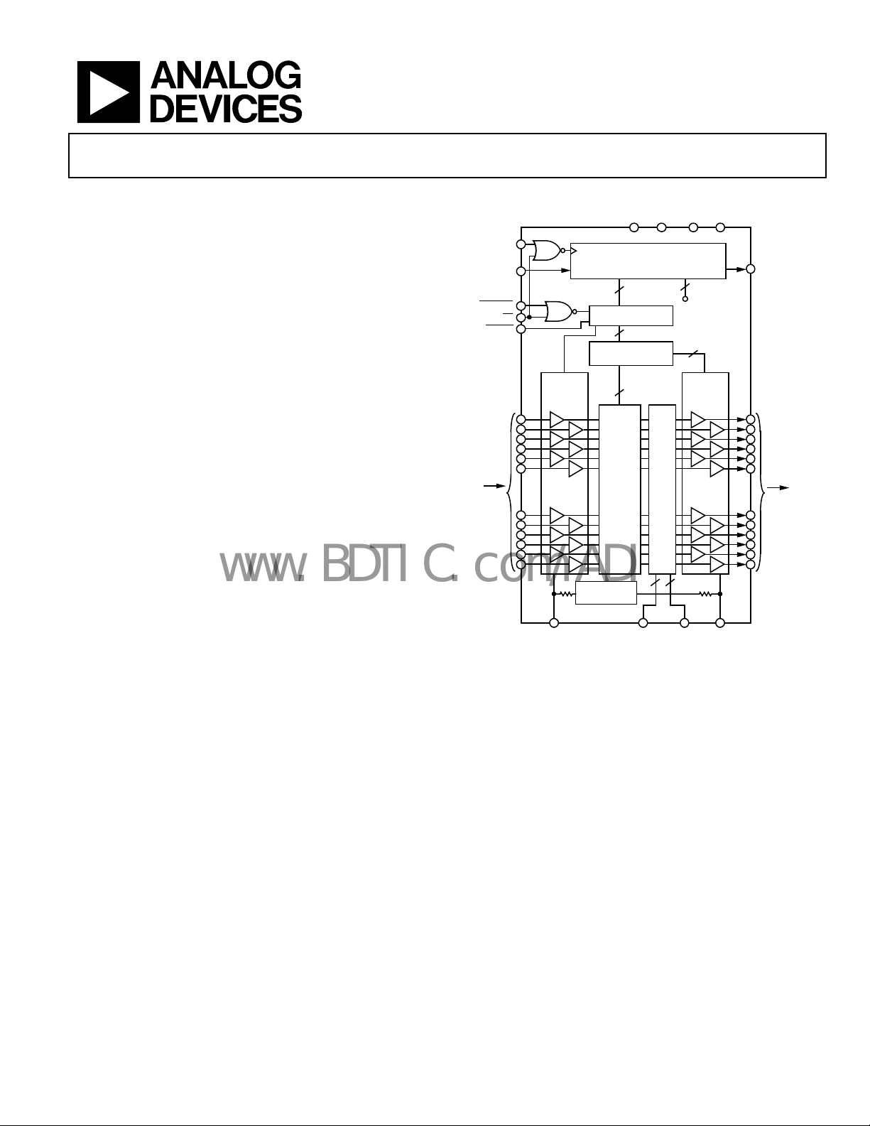
FUNCTIONAL BLOCK DIAGRAM
NEG DGNDDVCCPOS
CLK
193-BIT SHI FT REGISTER
OSD
MUX
SWITCHES
96
ADV3202
(ADV3203)
16
ENABLE/
DISABLE
OUTPUT
BUFFER
G = +1
(G = +2)
.
.
.
1616
OSD
.
.
.
CS
ENABLE/
BYPASS
SYNC-TIP
CLAMP
.
.
32
.
VCLAMP VREFOSD
PARALLEL L ATCH
.
.
.
REFERENCE
97
96
16 × 5:32
DECODERS
512
SWITCH
MATRIX
INPUTS
Figure 1.
DATA
OUT
16
OUTPUTS
07526-001
GENERAL DESCRIPTION
The ADV3202/ADV3203 are 32 × 16 analog crosspoint switch
matrices. They feature a selectable sync-tip clamp input for
ac-coupled applications and a 2:1 on-screen display (OSD)
insertion mux. With −48 dB of crosstalk and −80 dB isolation
at 5 MHz, the ADV3202/ADV3203 are useful in many high
density routing applications. The 0.1 dB flatness out to 60 MHz
makes the ADV3202/ADV3203 ideal for both composite and
component video switching.
The 16 independent output buffers of the ADV3202/ADV3203
can be placed into a high impedance state for paralleling crosspoint outputs so that off-channels present minimal loading to
Rev. 0
Information furnished by Analog Devices is believed to be accurate and reliable. However, no
responsibility is assumed by Analog Devices for its use, nor for any infringements of patents or other
rights of third parties that may result from its use. Specifications subject to change without notice. No
license is granted by implication or otherwise under any patent or patent rights of Analog Devices.
Trademarks and registered trademarks are the property of their respective owners.
an output bus if building a larger array. The ADV3202 has a
gain of +1 while the ADV3203 has a gain of +2 for ease of use in
back-terminated load applications. A single +5 V supply, dual
±2.5 V supplies, or dual ±3.3 V supplies (G = +2) can be used
while consuming only 195 mA of idle current with all outputs
enabled. The channel switching is performed via a double
buffered, serial digital control that can accommodate daisy
chaining of several devices.
The ADV3202/ADV3203 are packaged in a 176-lead exposed
pad LQFP package (24 mm× 24 mm) and are available over the
extended industrial temperature range of −40°C to +85°C.
One Technology Way, P.O. Box 9106, Norwood, MA 02062-9106, U.S.A.
Tel: 781.329.4700 www.analog.com
Fax: 781.461.3113 ©2008 Analog Devices, Inc. All rights reserved.

ADV3202/ADV3203
www.BDTIC.com/ADI
TABLE OF CONTENTS
Features .............................................................................................. 1
Applications ....................................................................................... 1
Functional Block Diagram .............................................................. 1
General Description ......................................................................... 1
Revision History ............................................................................... 2
Specifications ..................................................................................... 3
OSD Disabled ................................................................................ 3
OSD Enabled ................................................................................. 4
Timing Characteristics (Serial Mode) ....................................... 5
Absolute Maximum Ratings ............................................................ 6
Thermal Resistance ...................................................................... 6
REVISION HISTORY
10/08—Revision 0: Initial Version
Power Dissipation..........................................................................6
ESD Caution...................................................................................6
Pin Configuration and Function Descriptions ..............................7
Truth Table and Logic Diagram ............................................... 10
Typical Performance Characteristics ........................................... 11
Theory of Operation ...................................................................... 14
Applications Information .............................................................. 16
Programming .............................................................................. 16
Outline Dimensions ....................................................................... 17
Ordering Guide .......................................................................... 17
Rev. 0 | Page 2 of 20

ADV3202/ADV3203
www.BDTIC.com/ADI
SPECIFICATIONS
OSD DISABLED
VS = ±2.5 V (ADV3202), VS = ±3.3 V (ADV3203) at TA = 25°C, G = +1 (ADV3202), G = +2 (ADV3203), RL = 150 Ω, all configurations,
unless otherwise noted.
Table 1.
ADV3202/ADV3203
Parameter Conditions
DYNAMIC PERFORMANCE
−3 dB Bandwidth 200 mV p-p
2 V p-p 120 MHz
Gain Flatness 0.1 dB, 200 mV p-p 60 MHz
0.1 dB, 2 V p-p 40 MHz
Settling Time 1% , 2 V step 6 ns
Slew Rate 2 V step, peak 400 V/μs
NOISE/DISTORTION PERFORMANCE
Differential Gain Error NTSC or PAL 0.06/0.1 %
Differential Phase Error NTSC or PAL 0.06/0.03 Degrees
Crosstalk, All Hostile, RTI f = 5 MHz, RL = 150 Ω
= 1 kΩ
R
L
f = 100 MHz, RL = 150 Ω
= 1 kΩ
R
L
Off Isolation, Input-to-Output f = 5 MHz, one channel −80 dB
Input Voltage Noise 0.1 MHz to 50 MHz 25/22 nV/√Hz
DC PERFORMANCE
Gain Error Broadcast mode, no load ±0.5 ±1.75/±2.2 %
Broadcast mode ±0.5 ±2.2/±2.7 %
Gain Matching No load, channel-to-channel ±0.5/±0.8 ±2.8 %
Channel-to-channel ±0.5/±0.8 ±3.4 %
OUTPUT CHARACTERISTICS
Output Impedance DC, enabled 0.15 Ω
DC, disabled 900/3.2 1000/4 kΩ
Output Capacitance Disabled 3.7 pF
Output Voltage Range ADV3202
ADV3203
ADV3203, no output load
INPUT CHARACTERISTICS
Input Offset Voltage ±5 ±30 mV
Input Voltage Range ADV3202
ADV3203
ADV3203, no output load
Input Capacitance 3 pF
Input Resistance 1 4 MΩ
Input Bias Current
Sync-tip clamp disabled −10 −3 μA
SWITCHING CHARACTERISTICS
Enable On Time 50% update to 1% settling 50 ns
Switching Time, 2 V Step 50% update to 1% settling 40 ns
Switching Transient (Glitch) IN00 to IN31, RTI 300 mV p-p
Sync-tip clamp enabled,
= VCLAMP + 0.1 V
V
IN
Sync-tip clamp enabled,
= VCLAMP − 0.1 V
V
IN
−48
−23
−1.1 to +1.1
−1.5 to +1.5
−1.5 to +1.5
−1.1 to +1.1
−0.75 to +0.75
−0.75 to +0.75
0.1 3 12 μA
−2.9 −1 −0.25 mA
300 MHz
dB
−65
dB
−30
−1.2 to +1.2
−1.6 to +2.0
−2.0 to +2.0
−1.2 to +1.2
−0.8 to +1.0
−1.0 to +1.0
V
V
Unit Min Typ Max
dB
dB
V
V
V
V
Rev. 0 | Page 3 of 20

ADV3202/ADV3203
www.BDTIC.com/ADI
ADV3202/ADV3203
Parameter Conditions
POWER SUPPLIES
Supply Current
V
D
Supply Voltage Range V
PSR V
OPERATING TEMPERATURE RANGE
Temperature Range Operating (still air) −40 to +85 °C
θJA Operating (still air) 16 °C/W
or V
V
POS
no load
POS
VCC
POS
NEG
, outputs enabled,
NEG
or V
, outputs disabled 120/130 155/165 mA
NEG
2.5 3.5 mA
− V
NEG
, V
, f = 1 MHz −50/−45 dB
POS
195/200 220/235 mA
5 ± 10%/
6.6 ± 10%
V
OSD ENABLED
VS = ±2.5 V (ADV3202), VS = ±3.3 V (ADV3203) at TA = 25°C, G = +1 (ADV3202), G = +2 (ADV3203), RL = 150 Ω, all configurations,
unless otherwise noted.
Table 2.
ADV3202/ADV3203
Parameter Conditions
OSD DYNAMIC PERFORMANCE
−3 dB Bandwidth 200 mV p-p
2 V p-p 135/130 MHz
Gain Flatness 0.1 dB, 200 mV p-p 35 MHz
0.1 dB, 2 V p-p 35 MHz
Settling Time 1%, 2 V step 6 ns
Slew Rate 2 V step, peak 400 V/μs
OSD NOISE/DISTORTION PERFORMANCE
Differential Gain Error NTSC or PAL 0.12/0.35 %
Differential Phase Error NTSC or PAL 0.06/0.04 Degrees
Input Voltage Noise 0.5 MHz to 50 MHz 27/25 nV/√Hz
OSD DC PERFORMANCE
Gain Error No load ±0.1 ±2.3/±2.2 %
±0.1 ±2.7 %
OSD INPUT CHARACTERISTICS
Input Bias Current Sync-tip clamp disabled −10 −4 μA
OSD SWITCHING CHARACTERISTICS
OSD Switch Delay, 2 V Step 50% OSD switch to 1% settling 20 ns
OSD Switching Transient (Glitch) 15/40 mV p-p
170/150 MHz
Unit Min Typ Max
Unit Min Typ Max
Rev. 0 | Page 4 of 20

ADV3202/ADV3203
www.BDTIC.com/ADI
TIMING CHARACTERISTICS (SERIAL MODE)
Specifications subject to change without notice.
Table 3.
Limit
Parameter Symbol Min Typ Max Unit
Serial Data Setup Time t1 40 ns
CLK Pulse Width t2 50 ns
Serial Data Hold Time t3 50 ns
CLK Pulse Separation t4 150 ns
t
CLK to UPDATE Delay
UPDATE Pulse Width
CLK to DATA OUT Valid t7 130 ns
Propagation Delay, UPDATE to Switch On or Off
Data Load Time, CLK = 5 MHz, Serial Mode 38.6 μs
RESET Time
1
CS
0
t
2
3
t
7
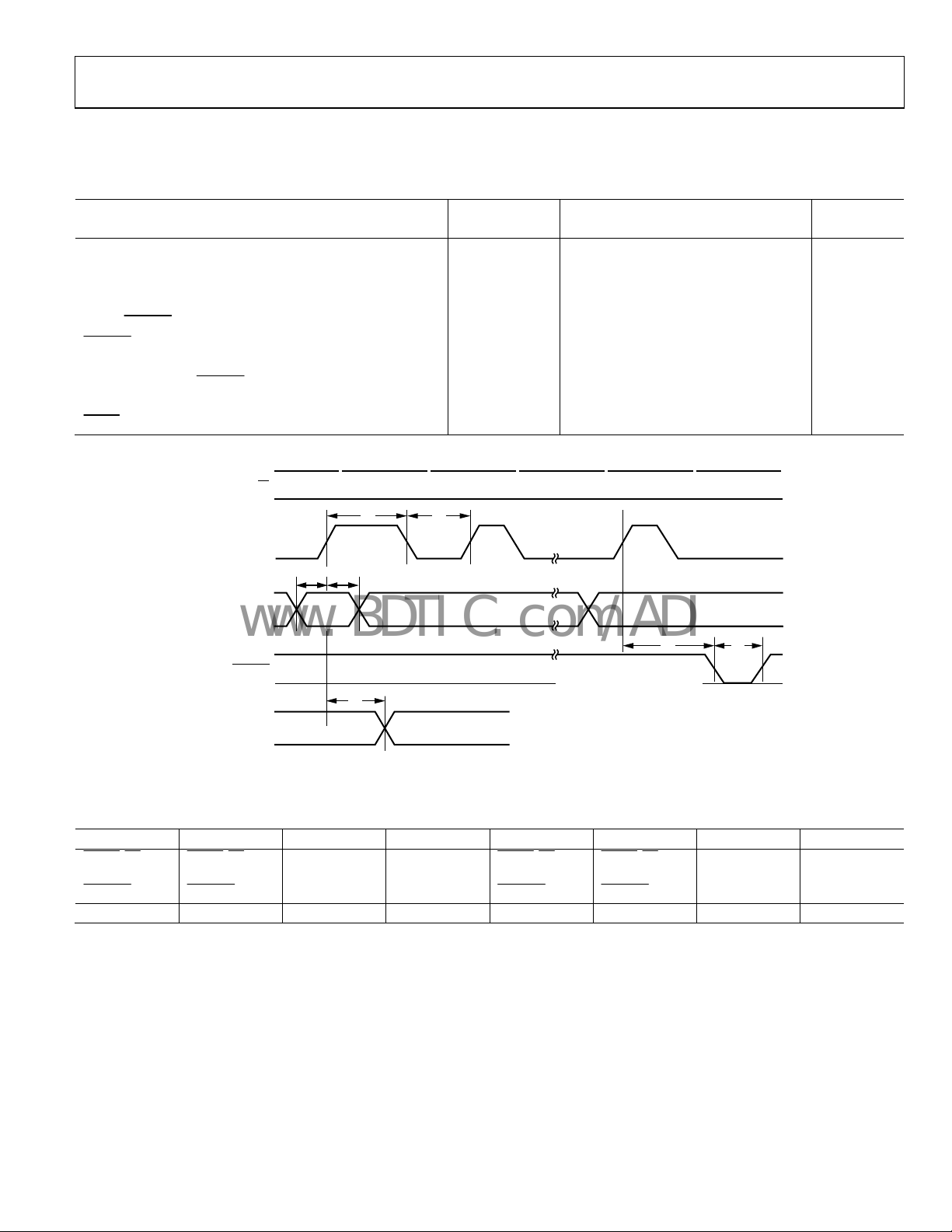
Figure 2. Timing Diagram, Serial Mode
CLK
DATA IN
1 = LATCHED
UPDATE
0 = TRANSPARENT
DATA OUT
1
0
t1t
1
0
CLAMP
ON/OFF
50 160 ns
5
t
40 ns
6
50 ns
160 ns
t
4
LOAD DATA INT O
SERIAL REGI STER
ON RISING E DGE
TRANSFER DATA FRO M SERIAL
REGISTER TO PARALLEL
LATCHES DURING LOW LE VEL
OUT00 (D0)OUT15 (D5)
t
5
t
6
7526-002
Table 4. Logic Levels, DVCC = 3.3 V
VIH VIL V
RESET, CS,
CLK, DATA IN,
UPDATE
, OSDS
RESET
, CS,
CLK, DATA IN,
UPDATE
, OSDS
V
OH
I
OL
DATA OUT DATA OUT
2.5 V min 0.8 V max 2.7 V min 0.5 V max 0.5 μA typ −0.5 μA typ 3 mA typ −3 mA typ
Rev. 0 | Page 5 of 20
I
IH
, CS,
RESET
CLK, DATA IN,
UPDATE
, OSDS
I
IL
RESET
, CS,
CLK, DATA IN,
UPDATE
, OSDS
I
OH
OL
DATA OUT DATA OUT

ADV3202/ADV3203
www.BDTIC.com/ADI
ABSOLUTE MAXIMUM RATINGS
Table 5.
Parameter Rating
Analog Supply Voltage (V
Digital Supply Voltage
(DVCC − D
GND
)
Ground Potential Difference
(V
− D
GND
)
NEG
Maximum Potential Difference
DVCC − V
9.4 V
NEG
Disabled Outputs
ADV3202 (|V
ADV3203 (|V
|V
− V
CLAMP
V
Input Voltage
REF
OSD
OSD
| 6 V
INxx
ADV3202 V
ADV3203 V
Analog Input Voltage V
Digital Input Voltage DVCC
Output Voltage
(Disabled Analog Output)
Output Short-Circuit Duration Momentary
Output Short-Circuit Current 45 mA
Storage Temperature Range −65°C to +125°C
Operating Temperature Range −40°C to +85°C
Lead Temperature
(Soldering, 10 sec)
Junction Temperature 150°C
− V
POS
) 7.5 V
NEG
6 V
+0.5 V to –4 V
− V
|) <3 V
OUT
−(V
OUT+VREF
)/2|) <3 V
(V
300°C
– 3.5 V to V
POS
– 4 V to V
POS
to V
NEG
− 1 V) to (V
POS
POS
+ 3.5 V
NEG
+ 4 V
NEG
+ 1 V)
NEG
POWER DISSIPATION
The ADV3202/ADV3203 are operated with ±2.5 V, +5 V, or
±3.3 V supplies and can drive loads down to 150 , resulting in
a large range of possible power dissipations. For this reason,
extra care must be taken while derating the operating conditions
based on ambient temperature.
Packaged in a 176-lead exposed-pad LQFP, the ADV3202/
ADV3203 junction-to-ambient thermal impedance (θ
16°C/W. For long-term reliability, the maximum allowed
junction temperature of the die should not exceed 150°C.
Temporarily exceeding this limit may cause a shift in parametric
performance due to a change in stresses exerted on the die by
the package. Exceeding a junction temperature of 175°C for an
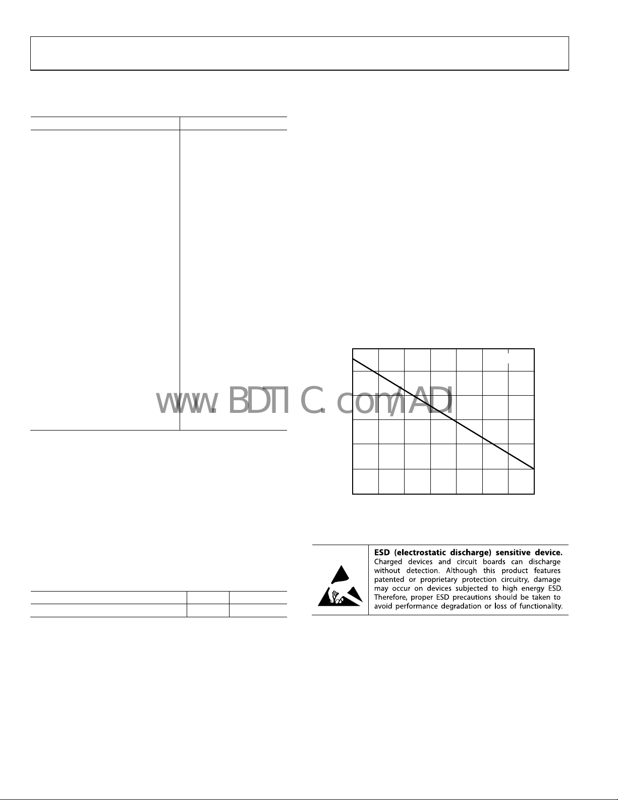
extended period can result in device failure. Figure 3 shows the
range of allowed internal die power dissipations that meet these
conditions over the −40°C to +85°C ambient temperature range.
When using Figure 3, do not include external load power in the
maximum power calculation, but do include load current
dropped on the die output transistors.
9
TJ = 150°C
8
7
6
JA
) is
Stresses above those listed under Absolute Maximum Ratings
may cause permanent damage to the device. This is a stress
rating only; functional operation of the device at these or any
other conditions above those indicated in the operational
section of this specification is not implied. Exposure to absolute
maximum rating conditions for extended periods may affect
device reliability.
THERMAL RESISTANCE
θJA is specified for the worst-case conditions, that is, a device
soldered in a circuit board for surface-mount packages.
Table 6. Thermal Resistance
Package Type θJA Unit
176-Lead LQFP_EP 16 °C/W
5
MAXIMUM POWER (W)
4
3
15 25 35 45 55 65 75 85
Figure 3. Maximum Die Power Dissipation vs. Ambient Temperature
AMBIENT TEM PERATURE (°C)
ESD CAUTION
07526-003
Rev. 0 | Page 6 of 20
 Loading...