www.BDTIC.com/ADI
JPEG 2000 Video Codec
FEATURES
Complete single-chip JPEG 2000 compression and
decompression solution for video and still images
Identical in pinout and footprint to the ADV202 and
supports all the functionality of the ADV202
Power reduction of at least 30% compared with ADV202
JTAG/boundary scan support
Patented SURF® (spatial ultraefficient recursive filtering)
technology enables low power, low cost wavelet-based
compression
Supports both 9/7 and 5/3 wavelet transforms with up to
6 levels of transform
Video interface directly supporting ITU-R BT.656,
SMPTE 125M PAL/NTSC, SMPTE 274M, SMPTE 293M
(525p), and ITU-R BT.1358 (625p), or any video format with
a maximum input rate of 65 MSPS for irreversible mode or
40 MSPS for reversible mode
Programmable tile/image size with widths up to 4096 pixels
in single-component mode; maximum tile/image height:
4096 pixels
2 or more ADV212s can be combined to support full-frame
SMPTE 274M HDTV (1080i) or SMPTE 296M (720p)
Flexible, asynchronous SRAM-style host interface allows glue-
less connection to most 16-/32-bit microcontrollers and ASICs
2.5 V or 3.3 V input/output and 1.5 V core supply
12 mm × 12 mm, 121-ball CSPBGA with a speed grade of
115 MHz, or 13 mm × 13 mm, 144-ball CSPBGA with a
speed grade of 150 MHz
APPLICATIONS
Networked video and image distribution systems
Wireless video and image distribution
Image archival/retrieval
Digital CCTV and surveillance systems
Digital cinema systems
Professional video editing and recording
Digital still cameras
Digital camcorders
ADV212
GENERAL DESCRIPTION
The ADV212 is a single-chip JPEG 2000 codec targeted for
video and high bandwidth image compression applications that
can benefit from the enhanced quality and features provided by
the JPEG 2000 (J2K)—ISO/IEC15444-1 image compression
standard. The part implements the computationally intensive
operations of the JPEG 2000 image compression standard and
provides fully compliant code-stream generation for most
applications.
The dedicated video port of the ADV212 provides glueless connection to common digital video standards such as ITU-R BT.656,
SMPTE 125M, SMPTE 293M (525p), ITU-R BT.1358 (625p),
SMPTE 274M (1080i), or SMPTE 296M (720p). A variety of
other high speed, synchronous pixel and video formats can also
be supported by using the programmable framing and
validation signals.
The ADV212 is an upgrade version of the ADV202 that is
identical in pinout and footprint. It supports all the functionality
of the ADV202 and has the following additional options:
• JTAG/boundary scan support
• Power reduction of at least 30% compared with the
ADV202
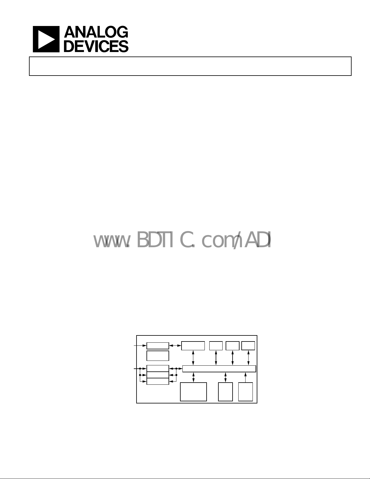
FUNCTIONAL BLOCK DIAGRAM
PIXEL I/F
HOST I/F
Rev. 0
Information furnished by Analog Devices is believed to be accurate and reliable. However, no
responsibility is assumed by Anal og Devices for its use, nor for any infringements of patents or ot her
rights of third parties that may result from its use. Specifications subject to change without notice. No
license is granted by implication or otherwise under any patent or patent rights of Analog Devices.
Trademarks and registered trademarks are the property of their respective owners.
PIXEL I/F
EXTERNAL
DMA CTRL
PIXEL FIFO
CODE FIF O
ATTR FIFO
ADV212
WAVELET
ENGINE
INTERNAL BUS AND DMA ENGINE
EMBEDDED
RISC
PROCESSOR
SYSTEM
Figure 1.
EC1 EC2 EC3
RAM ROM
06389-001
One Technology Way, P.O. Box 9106, Norwood, MA 02062-9106, U.S.A.
Tel: 781.329.4700 www.analog.com
Fax: 781.461.3113 ©2006 Analog Devices, Inc. All rights reserved.

ADV212
www.BDTIC.com/ADI
TABLE OF CONTENTS
Features.............................................................................................. 1
Applications....................................................................................... 1
General Description ......................................................................... 1
Revision History ............................................................................... 2
JPEG 2000 Feature Support......................................................... 3
Specificatons...................................................................................... 4
Supply Voltages and Current ...................................................... 4
Input/Output Specifications........................................................ 4
Clock and
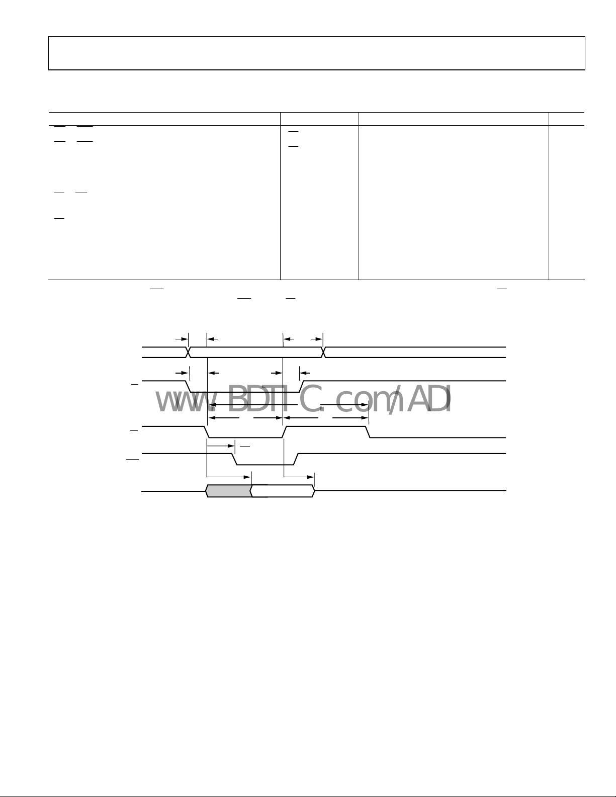
Normal Host Mode—Write Operation ..................................... 6
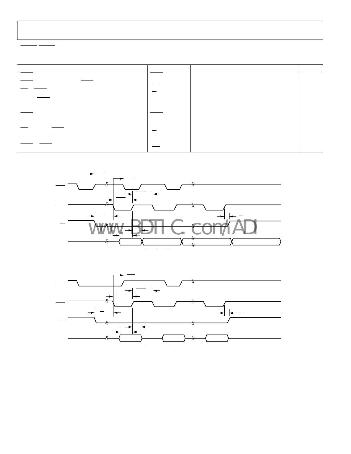
Normal Host Mode—Read Operation ...................................... 7
DREQ
DREQ
External DMA Mode—FIFO Write, Burst Mode .................. 12
External DMA Mode—FIFO Read, Burst Mode ................... 13
Streaming Mode (JDATA)—FIFO Read/Write...................... 14
VDATA Mode Timing............................................................... 15
Raw Pixel Mode Timing............................................................ 17
JTAG Timing............................................................................... 18
Absolute Maximum Ratings.......................................................... 19
Thermal Resistance .................................................................... 19
ESD Caution................................................................................ 19
Pin Configurations and Function Descriptions ......................... 20
Theory of Operation ...................................................................... 25
Wavelet Engine ........................................................................... 25
Entropy Codecs........................................................................... 25
Embedded Processor System.................................................... 25
RESET
Specifications................................................ 5
DACK
/
DMA Mode—Single FIFO Write Operation .. 8
DACK
/
DMA Mode—Single FIFO Read Operation. 10
Memory System.......................................................................... 25
Internal DMA Engine................................................................ 25
ADV212 Interface .......................................................................... 26
Video Interface (VDATA Bus).................................................. 26
Host Interface (HDATA Bus) ................................................... 26
Direct and Indirect Registers.................................................... 26
Control Access Registers........................................................... 27
Pin Configuration and Bus Sizes/Modes ................................ 27
Stage Register.............................................................................. 27
JDATA Mode............................................................................... 27
External DMA Engine ............................................................... 27
Internal Registers............................................................................ 28
Direct Registers........................................................................... 28
Indirect Registers........................................................................ 29
PLL ............................................................................................... 30
Hardware Boot............................................................................ 31
Video Input Formats ...................................................................... 32
Applications..................................................................................... 34
Encode—Multichip Mode......................................................... 34
Decode—Multichip Master/Slave ............................................ 35
Digital Still Camera/Camcorder .............................................. 36
Encode/Decode SDTV Video Application............................. 37
32-Bit Host Application............................................................. 38
HIPI (Host Interface—Pixel Interface) ................................... 39
JDATA Interface ......................................................................... 40
Outline Dimensions....................................................................... 41
Ordering Guide .......................................................................... 42
REVISION HISTORY
10/06—Revision 0: Initial Version
Rev. 0 | Page 2 of 44

ADV212
www.BDTIC.com/ADI
The ADV212 can process images at a rate of 40 MSPS in reversible
mode and at higher rates when used in irreversible mode. The
ADV212 contains a dedicated wavelet transform engine, three
entropy codecs, an on-board memory system, and an embedded
reduced instruction set computer (RISC) processor that can
provide a complete JPEG 2000 compression/decompression
solution.
The wavelet processor supports the 9/7 irreversible wavelet
transform and the 5/3 wavelet transform in reversible and
irreversible modes. The entropy codecs support all features in
the JPEG 2000 Part 1 specification, except maximum shift
region of interest (ROI).
The ADV212 operates on a rectangular array of pixel samples
called a tile. A tile can contain a complete image, up to the
maximum supported size, or some portion of an image. The
maximum horizontal tile size supported depends on the wavelet
transform selected and the number of samples in the tile.
Images larger than the ADV212’s maximum tile size can be
broken into individual tiles and then sent sequentially to the
chip while maintaining a single, fully compliant JPEG 2000
code stream for the entire image.
JPEG 2000 FEATURE SUPPORT
The ADV212 supports a broad set of features that are included
in Part 1 of the JPEG 2000 standard (ISO/IEC 15444). See
ADV212 User’s Guide f
that the ADV212 currently supports.
Depending on the particular application requirements, the
ADV212 can provide varying levels of JPEG 2000 compression
support. It can provide raw code block and attribute data output,
which allows the host software to have complete control over
the generation of the JPEG 2000 code stream and other aspects
of the compression process such as bit-rate control. Otherwise,
the ADV212 can create a complete, fully compliant JPEG 2000
code stream (J2C) and enhanced file formats such as JP2.
or information on the JPEG 2000 features
Rev. 0 | Page 3 of 44
ADV212
www.BDTIC.com/ADI
SPECIFICATONS
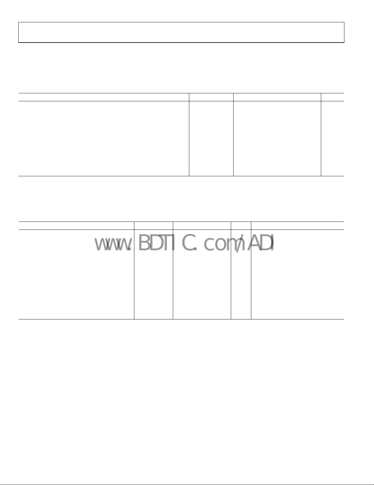
Specifications apply to IOVDD = 2.5 V or 3.3 V over operating temperature range, unless otherwise specified.
SUPPLY VOLTAGES AND CURRENT
Table 1.
Parameter Mnemonic Min Typ Max Unit
DC Supply Voltage, Core VDD 1.425 1.5 1.575 V
DC Supply Voltage, Input/Output IOVDD 2.375 2.5 2.625 V
DC Supply Voltage, Input/Output IOVDD 3.135 3.3 3.465 V
Input Range VIN −0.3 V
Operating Ambient Temperature Range in Free Air T −40 +25 +85 °C
Static Current1 IDD 15 30 mA
Dynamic Current, Core (JCLK Frequency = 150 MHz)2 380 440 mA
Dynamic Current, Core (JCLK Frequency = 108 MHz) 280 320 mA
Dynamic Current, Core (JCLK Frequency = 81 MHz) 210 290 mA
Dynamic Current, Input/Output 40 50 mA
1
No clock or input/output activity.
2
ADV212-150 only.
INPUT/OUTPUT SPECIFICATIONS
+ 0.3 V
DDI/O
Table 2.
Parameter Mnemonic Min Typ Max Unit Test Conditions
High Level Input Voltage V
High Level Input Voltage V
Low Level Input Voltage V
High Level Output Voltage V
High Level Output Voltage V
Low Level Output Voltage V
High Level Input Current IIH 1.0 μA VDD = maximum, VIN = VDD
Low Level Input Current IIL 1.0 μA VDD = maximum, VIN = 0 V
High Level Three-State Leakage Current I
Low Level Three-State Leakage Current I
Input Pin Capacitance CI 8 pF
Output Pin Capacitance CO 8 pF
2.2 V VDD = maximum
IH (3.3 V)
1.9 V VDD = maximum
IH (2.5 V)
IL (3.3 V, 2.5 V )
OH (3.3 V)
OH (2.5 V)
OL (3.3 V, 2.5 V )
OZH
OZL
0.6 V VDD = minimum
2.4 V VDD = minimum, IOH = −0.5 mA
2.0 V VDD = minimum, IOH = −0.5 mA
0.4 V VDD = minimum, IOL = +2 mA
1.0 μA VDD = maximum, VIN = VDD
1.0 μA VDD = maximum, VIN = 0V
Rev. 0 | Page 4 of 44
ADV212
www.BDTIC.com/ADI
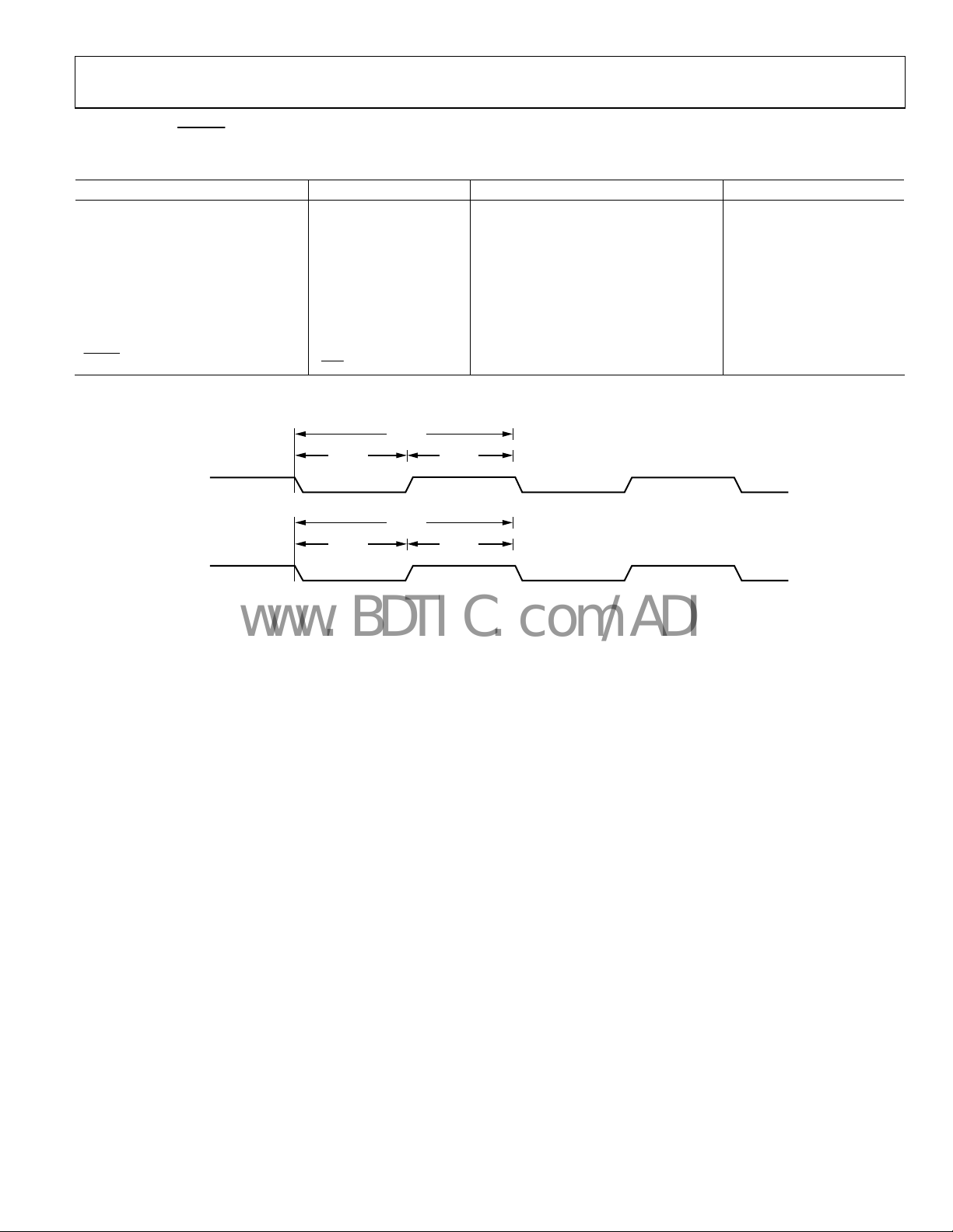
CLOCK AND RESET SPECIFICATIONS
Table 3.
Parameter Mnemonic Min Typ Max Unit
MCLK Period t
MCLK Frequency f
MCLK Width Low t
MCLK Width High t
VCLK Period t
VCLK Frequency f
VCLK Width Low t
VCLK Width High t
RESET Width Low
1
For a definition of MCLK, see Figure 32.
MCLK
13.3 100 ns
MCLK
10 75.18 MHz
MCLK
6 ns
MCLKL
6 ns
MCLKH
13.4 50 ns
VCLK
20 74.60 MHz
VCLK
5 ns
VCLKL
5 ns
VCLKH
t
5 MCLK cycles1
RESET
t
MCLK
VCLK
t
MCLKH
t
VCLKH
t
MCLKL
t
VCLKL
t
VCLK
Figure 2. Input Clock
06389-010
Rev. 0 | Page 5 of 44
ADV212
A
www.BDTIC.com/ADI
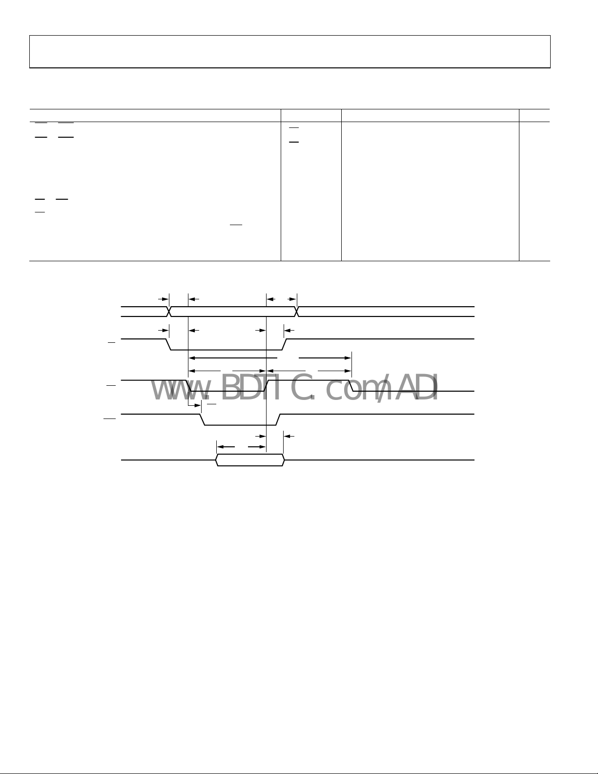
NORMAL HOST MODE—WRITE OPERATION
Table 4.
Parameter Mnemonic Min Typ Max Unit
t
WE to ACK, Direct Registers and FIFO Accesses
WE to ACK, Indirect Registers
Data Setup tSD 3.0 ns
Data Hold tHD 1.5 ns
Address Setup tSA 2 ns
Address Hold t
CS to WE Setup
CS Hold
Write Inactive Pulse Width (Minimum Time Until Next WE Pulse)
Write Active Pulse Width tWL 2.5 JCLK ns
Write Cycle Time t
1
For a definition of JCLK, see Figure 32.
t
SA
ADDR
(direct) 5 1.5 × JCLK + 7.0 ns
ACK
t
(indirect) 5 2.5 × JCLK + 7.0 ns
ACK
2 ns
HA
t
0 ns
SC
t
0 ns
HC
t
2.5 JCLK1 ns
WH
5 JCLK ns
WCYC
t
HA
ACK
HDAT
CS
WE
t
SC
t
WL
t
ACK
t
SD
VALID
t
HC
t
WCYC
t
WH
t
HD
06389-012
Figure 3. Normal Host Mode—Write Operation
Rev. 0 | Page 6 of 44
ADV212
www.BDTIC.com/ADI
NORMAL HOST MODE—READ OPERATION
Table 5.
Parameter Mnemonic Min Typ Max Unit
RD to ACK, Direct Registers and FIFO Accesses
RD to ACK, Indirect Registers
Read Access Time, Direct Registers t
Read Access Time, Indirect Registers t
Data Hold t
CS to RD Setup
t
ACK
t
ACK
DRD
DRD
HZRD
t
0 ns
SC
Address Setup tSA 2 ns
t
CS Hold
Address Hold t
0 ns
HC
2 ns
HA
Read Inactive Pulse Width tRH 2.5 JCLK 2 ns
Read Active Pulse Width tRL 2.5 JCLK ns
Read Cycle Time, Direct Registers t
1
Timing relationship between
minimum of three JCLK cycles is recommended between
2
For a definition of JCLK, see Figure 32.
ACK
falling transition and HDATA valid is not guaranteed. HDATA valid hold time is guaranteed with respect to RD rising transition. A
ACK
assert and RD deassert.
RCYC
t
SA
ADDR
1
(direct)
(indirect)
1
5 1.5 × JCLK + 7.0 ns
10.5 × JCLK 15.5 × JCLK + 7.0 ns
(direct) 5 1.5 × JCLK + 7.0 ns
(indirect) 10.5 × JCLK 15.5 × JCLK + 7.0 ns
2 8.5 ns
5.0 JCLK ns
t
HA
CS
RD
ACK
HDATA
t
SC
t
RL
t
ACK
t
DRD
VALID
t
HC
t
RCYC
t
RH
t
HZRD
06389-011
Figure 4. Normal Host Mode—Read Operation
Rev. 0 | Page 7 of 44
ADV212
A
A
www.BDTIC.com/ADI
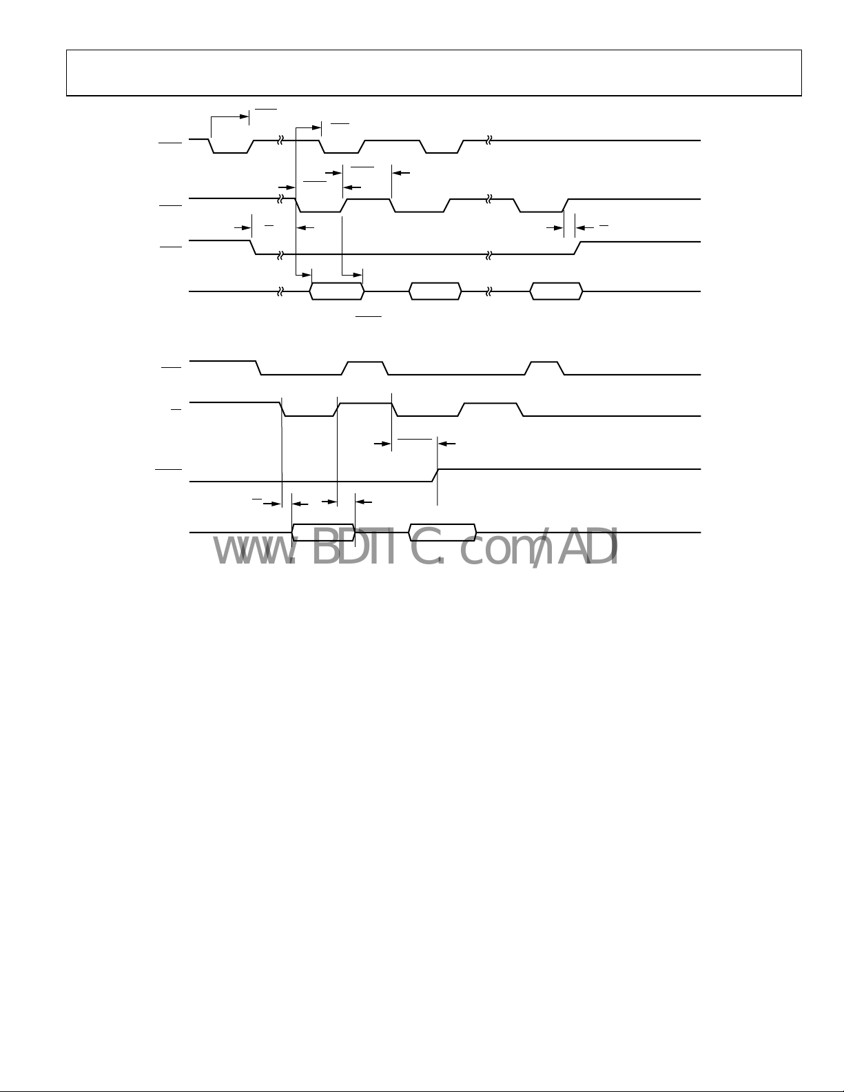
DREQ/DACK DMA MODE—SINGLE FIFO WRITE OPERATION
Table 6.
Parameter Mnemonic Min Typ Max Unit
DREQ Pulse Width DREQ
DACK Assert to Subsequent DREQ Delay
WE to DACK Setup
Data to DACK Deassert Setup
Data to DACK Deassert Hold
t
DREQ
t
WE
t
SU
t
HD
PULSE
2.5 JCLK 3.5 × JCLK + 8.5 ns
0 ns
SU
2 ns
2 ns
DACK Assert Pulse Width DACKLO
DACK Deassert Pulse Width DACKHI
t
WE Hold After DACK Deassert
0 ns
WE
HD
WE Assert to FSRQ Deassert (FIFO Full) WFSRQ
t
DACK to DREQ Deassert (DR × PULS = 0)
1
For a definition of JCLK, see Figure 32.
2.5 JCLK 3.5 × JCLK + 9.0 ns
DREQ
RTN
DREQ
DREQ
DACK
HDAT
WE
PULSE
t
WESU
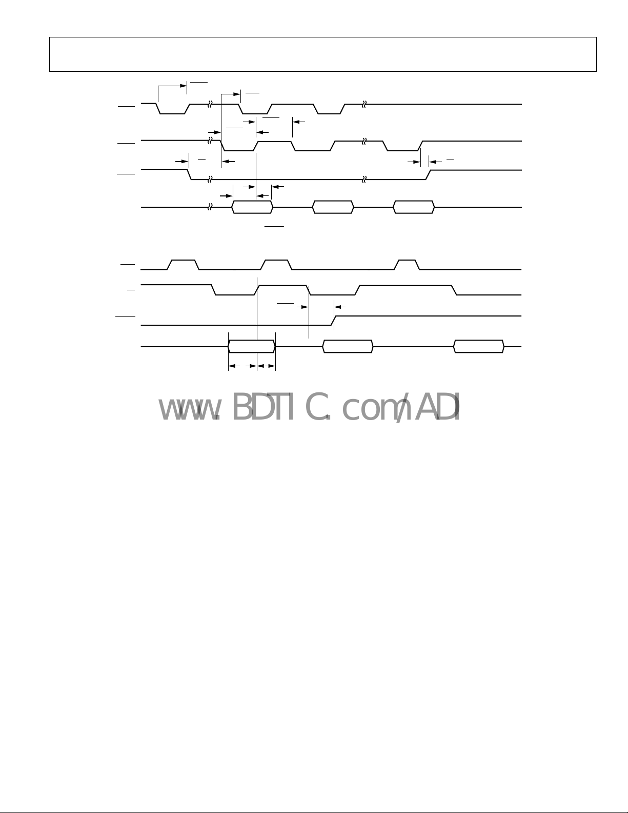
Figure 5. Single Write for
DACK
t
DREQ
DACK
HI
LO
t
HD
t
SU
DACK
DREQ
/
DMA Mode for Assigned DMA Channel
(EDMOD0/EDMOD1 <14:11> Not Programmed to a Value of 0000)
t
DREQRTN
DREQ
DACK
HI
t
HD
0 1 2
DACK
DREQ
/
DMA Mode for Assigned DMA Channel
DACK
HDAT
WE
DACK
LO
t
WESU
t
SU
Figure 6. Single Write for
(EDMOD0/EDMOD1 <14:11> Programmed to a Value of 0000)
1
1 JCLK
15 JCLK ns
2 JCLK ns
2 JCLK ns
1.5 JCLK 2.5 × JCLK + 7.5 ns
t
WEHD
t
WEHD
3210
6389-013
06389-014
Rev. 0 | Page 8 of 44
ADV212
A
A
www.BDTIC.com/ADI
DREQ
DREQ
DACK
WEFB
HDAT
t
WESU
PULSE
t
DREQ
DACK
DACK
LO
t
SU
HI
t
HD
0 1 2
t
WEHD
06389-015
Figure 7. Single Write Cycle for Fly-By DMA Mode
DREQ
(
Pulse Width Is Programmable)
FCS0
RD
WFSRQ
0
SUtHD
1 2
Figure 8. Single Write Access for DCS DMA Mode
FIFO FULL
NOT WRITTEN TO FIFO
6389-021
FSRQ0
HDAT
FIFO NOT FULL
t
Rev. 0 | Page 9 of 44
ADV212
A
A
www.BDTIC.com/ADI
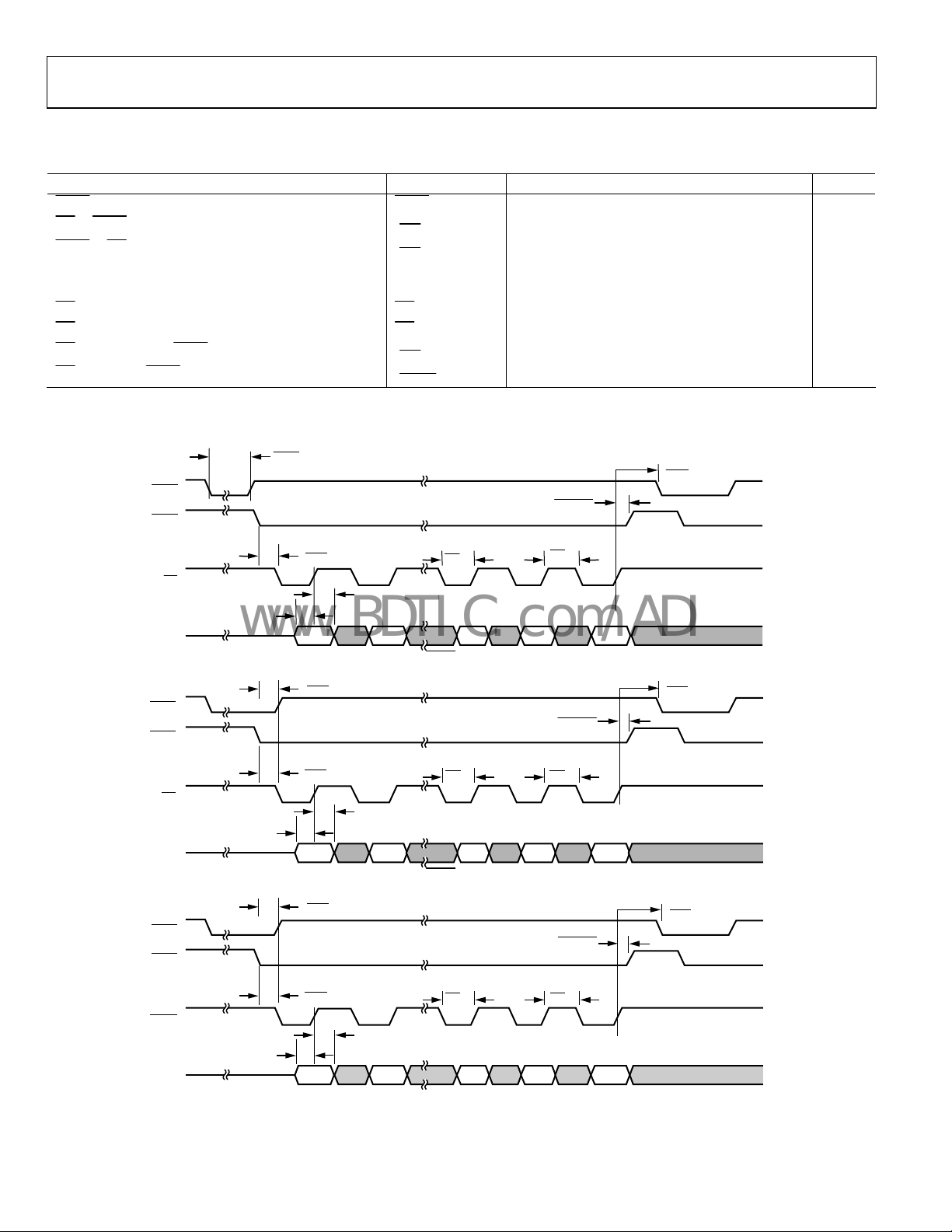
DREQ/DACK DMA MODE—SINGLE FIFO READ OPERATION
Table 7.
Parameter Mnemonic Min Typ Max Unit
DREQ Pulse Width DREQ
DACK Assert to Subsequent DREQ Delay
RD to DACK Setup
DACK to Data Valid
t
t
t
DREQ
RD
RD
PULSE
2.5 JCLK 3.5 × JCLK + 9.0 ns
0 ns
SU
2.5 11 ns
Data Hold tHD 1.5 ns
DACK Assert Pulse Width DACKLO
DACK Deassert Pulse Width DACKHI
t
RD Hold after DACK Deassert
0 ns
RD
HD
RD Assert to FSRQ Deassert (FIFO Empty) RDFSRQ
t
DACK to DREQ Deassert (DR × PULS = 0)
1
For a definition of JCLK, see Figure 32.
2.5 JCLK
DREQ
RTN
DREQ
PULSE
DREQ
DACK
t
DREQ
LO
DACK
HI
1
1 JCLK
15 JCLK ns
2 JCLK ns
2 JCLK ns
1.5 JCLK
2.5 × JCLK + 9.0
3.5 × JCLK + 9.0
ns
ns
DACK
HDAT
RD
t
RDSU
t
RD
0 1 2
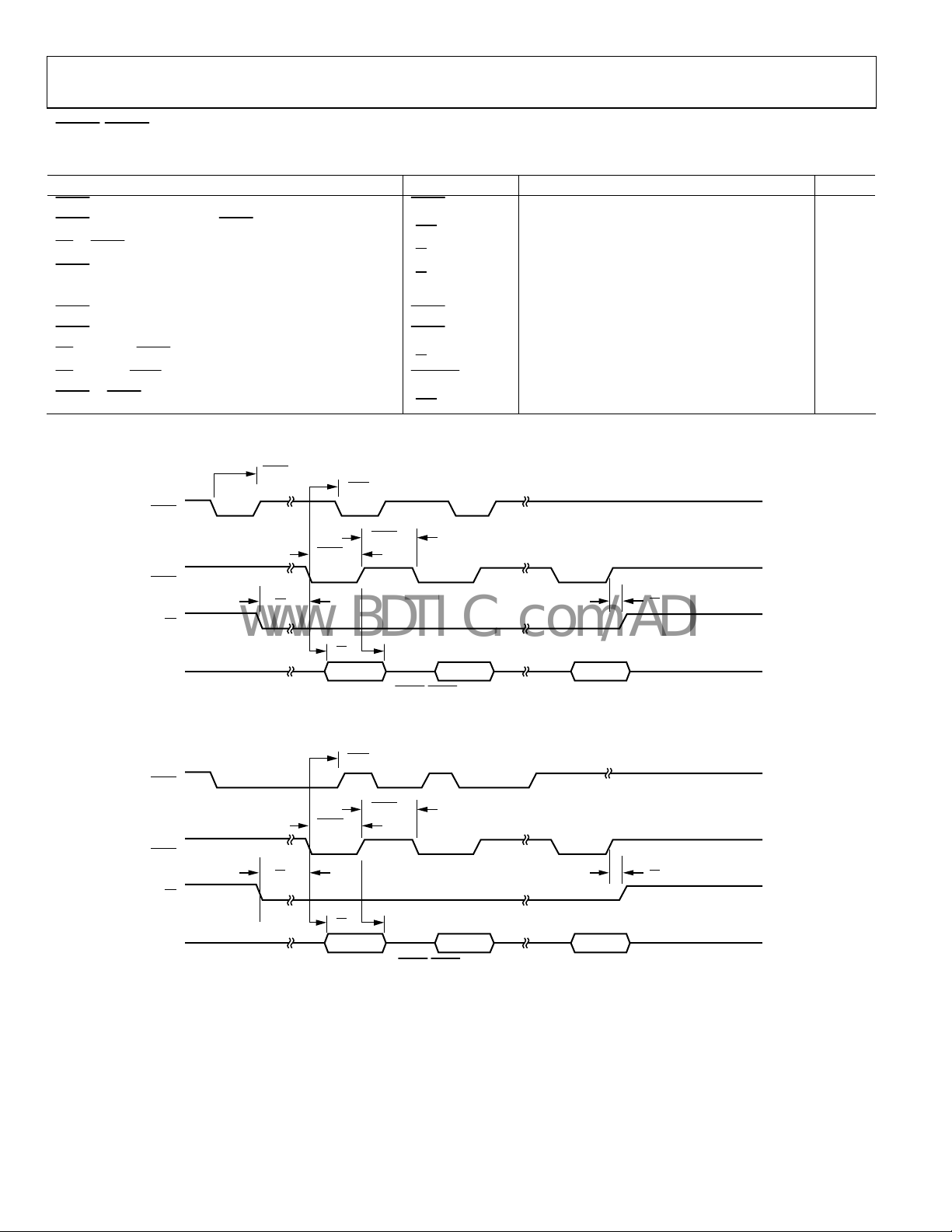
Figure 9. Single Read for
t
HD
DREQ
DACK
/
DMA Mode for Assigned DMA Channel
t
RDHD
6389-018
(EDMOD0/EDMOD1 <14:11> Not Programmed to a Value of 0000)
t
DREQRTN
DREQ
DACK
HI
t
HD
0 1 2
DACK
DREQ
/
DMA Mode for Assigned DMA Channel
t
RDHD
06389-019
DACK
HDAT
RD
DACK
LO
t
RDSU
t
RD
Figure 10. Single Read for
(EDMOD0/EDMOD1 <14:11> Programmed to a Value of 0000)
Rev. 0 | Page 10 of 44
ADV212
A
www.BDTIC.com/ADI
DREQ
DACK
RDFB
HDAT
DREQ
t
RDSU
PULSE
t
DREQ
DACK
DACK
LO
t
RD
HI
t
HD
0 1 2
t
RDHD
6389-020
Figure 11. Single Read Cycle for Fly-By DMA Mode
DREQ
(
Pulse Width Is Programmable)
FCS0
RD
RDFSRQ
FSRQ0
FIFO NOT EMPTY
t
RD
FIFO EMPTY
t
HD
HDATA
0
Figure 12. Single Read Access for DCS DMA Mode
1
6389-090
Rev. 0 | Page 11 of 44
ADV212
A
A
www.BDTIC.com/ADI
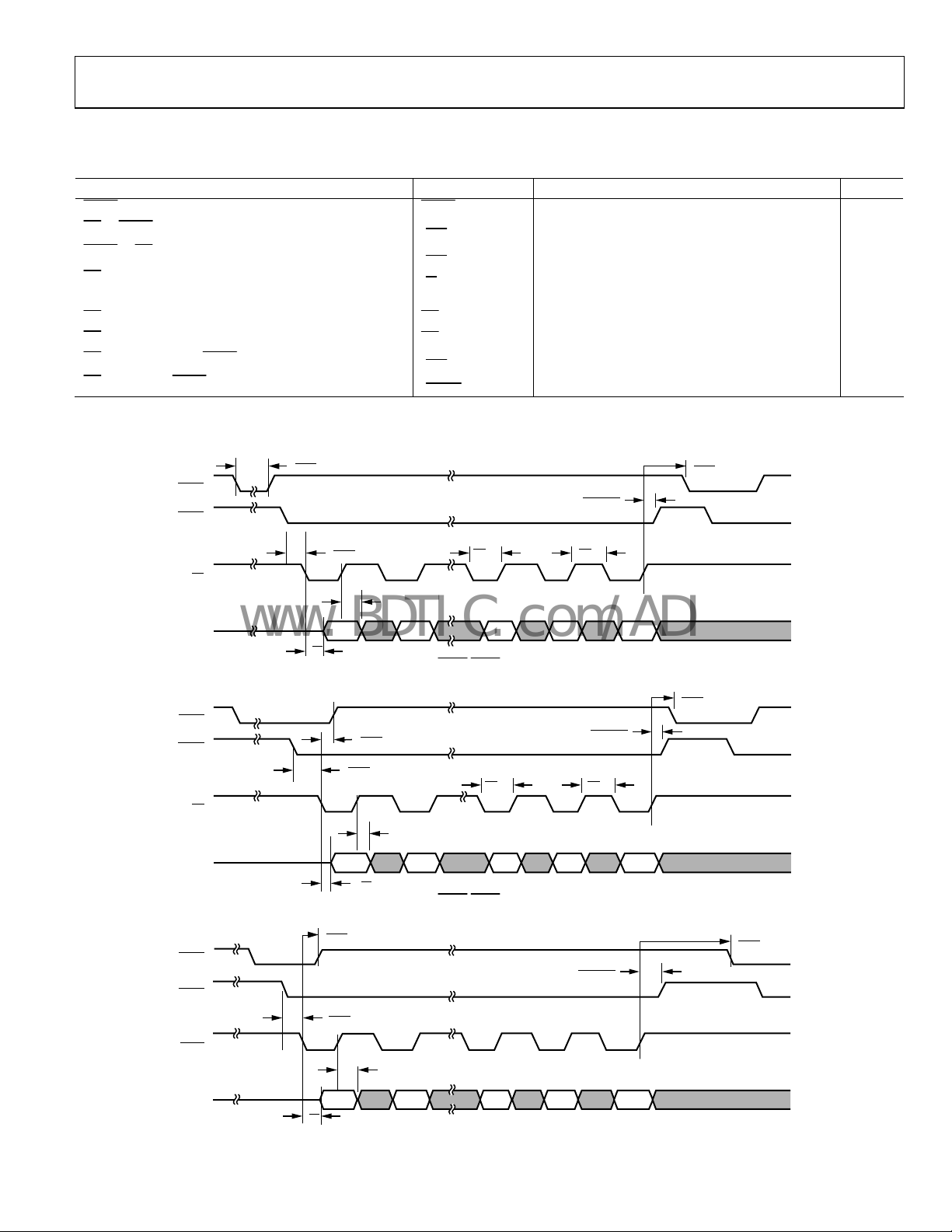
EXTERNAL DMA MODE—FIFO WRITE, BURST MODE
Table 8.
Parameter Mnemonic Min Typ Max Unit
DREQ Pulse Width1 DREQ
WE to DREQ Deassert (DR × PULS = 0)
DACK to WE Setup
t
t
DREQ
DACK
PULSE
2.5 JCLK 3.5 × JCLK + 7.5 ns
RTN
0 ns
SU
Data Setup tSU 2.5 ns
Data Hold tHD 2 ns
WE Assert Pulse Width WELO
WE Deassert Pulse Width WEHI
t
WEDeassert to Next DREQ
WE Deassert to DACK Deassert
1
Applies to assigned DMA channel, if EDMOD0 or EDMOD1 <14:11> is programmed to a nonzero value.
2
For a definition of JCLK, see Figure 32.
2.5 JCLK 4.5 × JCLK + 9.0 ns
DREQ
WAIT
t
WE_DACK
DREQ
PULSE
DREQ
DACK
2
1 JCLK
15 JCLK ns
1.5 JCLK ns
1.5 JCLK ns
0 ns
t
DREQWAIT
t
WE_DACK
WE
HDATA
DREQ
DACK
WE
HDAT
DREQ
DACK
WEFB
HDAT
t
DACKSU
t
HD
t
SU
01 13
Figure 13. Burst Write Cycle for
WE
DREQ
/DMA Mode for Assigned DMA Channel
LO
WE
HI
14 15
(EDMOD0/EDMOD1 <14:11> Not Programmed to a Value of 0000)
t
DREQRTN
t
WE_DACK
t
DACKSU
t
HD
t
SU
0 1 13 14 15
Figure 14. Burst Write Cycle for
WE
LO
DREQ
/DMA Mode for Assigned DMA Channel
WE
HI
(EDMOD0/EDMOD1 <14:11> Programmed to a Value of 0000)
t
DREQRTN
t
WE_DACK
t
DACKSU
t
HD
t
SU
0 1 13 14 15
WE
LO
WE
HI
Figure 15. Burst Write Cycle for Fly-By DMA Mode
t
DREQWAIT
t
DREQWAIT
06389-022
06389-023
6389-024
Rev. 0 | Page 12 of 44
ADV212
A
A
A
www.BDTIC.com/ADI
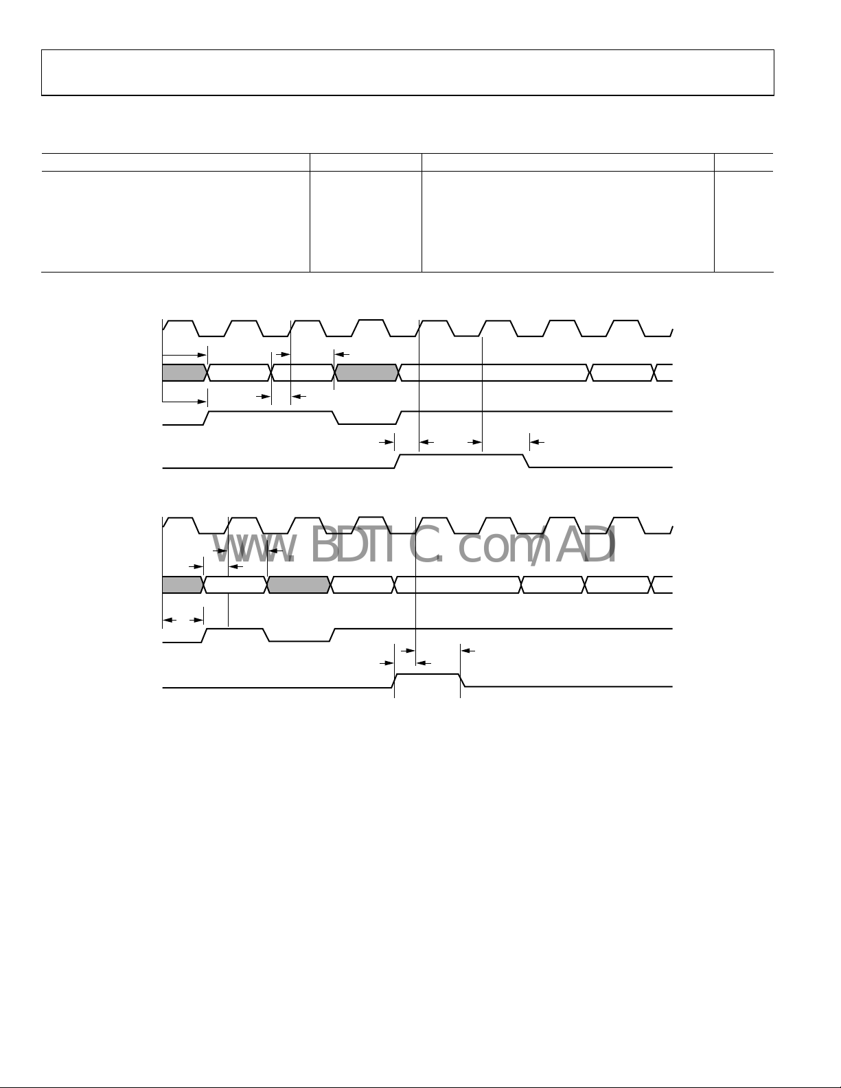
EXTERNAL DMA MODE—FIFO READ, BURST MODE
Table 9.
Parameter Mnemonic Min Typ Max Unit
DREQ Pulse Width1 DREQ
RD to DREQ Deassert (DR × PULS = 0)
DACK to RD Setup
RD to Data Valid
t
DREQ
t
DACK
t
RD
PULSE
2.5 JCLK 3.5 × JCLK + 7.5 ns
RTN
0 ns
SU
2.5 9.7 ns
Data Hold tHD 2.5 ns
RD Assert Pulse Width
RD Deassert Pulse Width
RD Deassert to Next DREQ
RD Deassert to DACK Deassert
1
Applies to assigned DMA channel if EDMOD0 or EDMOD1 <14:11> is programmed to a nonzero value.
2
For a definition of JCLK, see Figure 32.
RD
LO
RD
HI
t
2.5 JCLK 3.5 × JCLK + 7.5 ns
DREQ
WAIT
t
RD_DACK
t
DREQPULSE
DREQ
DACK
2
1 JCLK
15 JCLK ns
1.5 JCLK ns
1.5 JCLK ns
0 ns
t
DREQWAIT
t
RD_DACK
HDAT
DREQ
DACK
HDAT
DREQ
DACK
RD
RD
t
DACKSU
t
HD
0 1 13 14 15
t
RD
Figure 16. Burst Read Cycle for
(EMOD0/EDMOD1 <14:11> Not Programmed to a Value of 0
t
DREQRTN
t
DACKSU
t
HD
0 1 13 14 15
t
RD
Figure 17. Burst Read Cycle for
(EMOD0/EDMOD1 <14:11> Programmed to a Value of 0000)
t
DREQRTN
t
DACKSU
DREQ
DREQ
RD
LO
DACK
/
DMA Mode for Assigned DMA Channel
RD
LO
DACK
/
DMA Mode for Assigned DMA Channel
RD
HI
t
RD_DACK
RD
t
RD_DACK
HI
t
DREQWAIT
t
DREQWAIT
06389-025
06389-026
RDFB
t
HD
HDAT
0 1 13 14 15
t
RD
RD
Figure 18. Burst Read Cycle for Fly-By DMA Mode
Rev. 0 | Page 13 of 44
06389-027
ADV212
A
A
www.BDTIC.com/ADI
STREAMING MODE (JDATA)—FIFO READ/WRITE
Table 10.
Parameter Mnemonic Min Typ Max Unit
MCLK to JDATA Valid JDATATD 1.5 JCLK1 2.5 × JCLK + 9.5 ns
MCLK to VALID Assert/Deassert VALIDTD 1.5 JCLK 2.5 × JCLK + 8.0 ns
HOLD Setup to Rising MCLK HOLDSU 3 ns
HOLD Hold from Rising MCLK HOLDHD 3 ns
JDATA Setup to Rising MCLK JDATASU 3 ns
JDATA Hold from Rising MCLK JDATAHD 3 ns
1
For a definition of JCLK, see Figure 32.
MCLK
JDATA
JDATA
HD
SU
JDAT
VALID
JDATA
VALID
TD
TD
HOLD
HD
06389-028
HOLD
HOLD
SU
Figure 19. Streaming Mode Timing—Encode Mode JDATA Output
MCLK
JDATA
HD
HOLD
HOLD
SU
HD
06389-029
JDAT
VALID
HOLD
JDATA
VALID
SU
TD
Figure 20. Streaming Mode Timing—Decode Mode JDATA Input
Rev. 0 | Page 14 of 44
 Loading...