ANALOG DEVICES ADuM6400, ADuM6401, ADuM6402, ADuM6403, ADuM6404 Service Manual
Quad-Channel, 5 kV Isolators with
V
VOCV
V
V
V
V
V
V
V
V
Data Sheet
ADuM6400/ADuM6401/ADuM6402/ADuM6403/ADuM6404
FEATURES
isoPower integrated, isolated dc-to-dc converter
Regulated 5 V or 3.3 V output
Up to 400 mW output power
16-lead SOIC wide body package (RW-16)
16-lead SOIC wide body package with enhanced
creepage (RI-16-1)
Quad dc-to-25 Mbps (NRZ) signal isolation channels
Schmitt triggered inputs
High temperature operation: 105°C maximum
High common-mode transient immunity: >25 kV/μs
Safety and regulatory approvals (RI-16-1 package)
UL recognition
5000 V rms for 1 minute per UL 1577
CSA Component Acceptance Notice #5A (pending)
IEC 60601-1: 250 V rms
IEC 60950-1: 400 V rms
VDE certificate of conformity
DIN V VDE V 0884-10 (VDE V 0884-10):2006-12
V
= 846 V peak
IORM
APPLICATIONS
RS-232/RS-422/RS-485 transceivers
Medical isolation
AC/DC power supply start-up bias and gate drives
Isolated sensor interfaces
GENERAL DESCRIPTION
The ADuM6400/ADuM6401/ADuM6402/ADuM6403/
ADuM6404
an integrated, isolated dc-to-dc converter. Based on the Analog
Devices, Inc., iCoupler® technology, the dc-to-dc converter provides
up to 400 mW of regulated, isolated power at either 5.0 V or 3.3 V
from a 5.0 V input supply, or at 3.3 V from a 3.3 V supply at the
power levels shown in Table 1. These devices eliminate the need
for a separate, isolated dc-to-dc converter in low power, isolated
designs.
The ADuM6400/ADuM6401/ADuM6402/ADuM6403/
ADuM6404 isolators provide four independent isolation
channels in a variety of channel configurations and data rates
(see the Ordering Guide for more information).
isoPower uses high frequency switching elements to transfer power
through its transformer. Special care must be taken during printed
circuit board (PCB) layout to meet emissions standards. See the
AN-0971 Application Note for board layout recommendations.
1
Protected by U.S. Patents 5,952,849; 6,873,065; 6,903,578; and 7,075,329.
Rev. A
Information furnished by Analog Devices is believed to be accurate and reliable. However, no
responsibility is assumed by Analog Devices for its use, nor for any infringements of patents or other
rights of third parties that may result from its use. Specifications subject to change without notice. No
license is granted by implication or otherwise under any patent or patent rights of Analog Devices.
Trademarks and registered trademarks are the property of their respective owners.
1
are quad-channel digital isolators with isoPower®,
Integrated DC-to-DC Converter
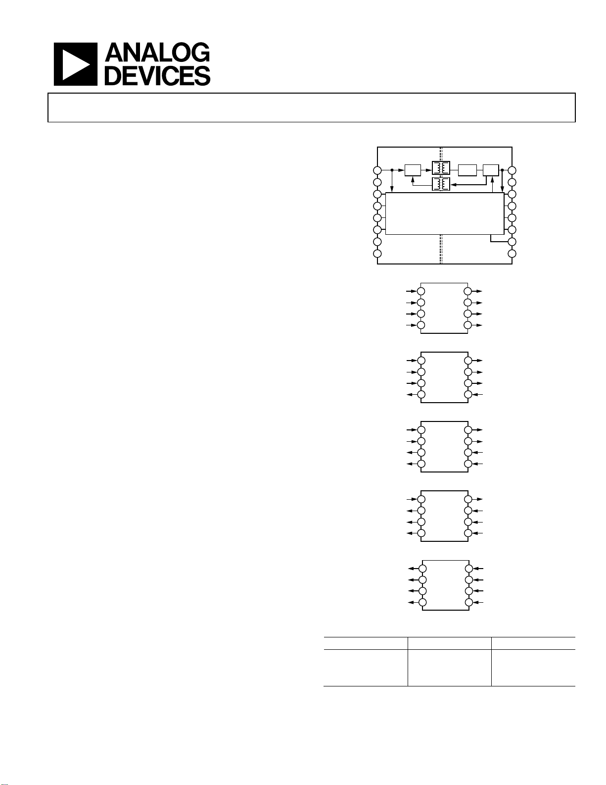
FUNCTIONAL BLOCK DIAGRAMS
OSC
4-CHANNEL iCOUPLER CORE
ADuM6400/ADuM6401/
ADuM6402/ADuM6403/
ADuM6404
V
IA
3
V
IB
4
V
ADuM6400
IC
5
V
ID
6
GND
VIA/V
VIB/V
VIC/V
VID/V
GND
1
V
DD1
2
1
3
OA
4
OB
5
OC
6
OD
7
V
DDL
8
1
Figure 2. ADuM6400
V
IA
3
V
IB
4
V
ADuM6401
IC
5
OD
6
Figure 3. ADuM6401
V
IA
3
V
IB
4
ADuM6402
5
OD
6
Figure 4. ADuM6402
V
IA
3
OB
4
ADuM6403
OC
5
OD
6
Figure 5. ADuM6403
OA
3
OB
4
ADuM6404
OC
5
OD
6
Figure 6. ADuM6404
Table 1. Power Levels
Input Voltage Output Voltage Output Power
5.0 V 5.0 V 400 mW
5.0 V 3.3 V 330 mW
3.3 V 3.3 V 132 mW
One Technology Way, P.O. Box 9106, Norwood, MA 02062-9106, U.S.A.
Tel: 781.329.4700 www.analog.com
Fax: 781.461.3113 ©2009–2012 Analog Devices, Inc. All rights reserved.
Figure 1.
RECT
14
13
12
11
14
13
12
11
14
13
12
11
14
13
12
11
14
13
12
11
REG
16
V
ISO
15
GND
ISO
VIA/V
14
OA
VIB/V
13
OB
VIC/V
12
OC
VID/V
11
OD
10
V
SEL
GND
9
ISO
V
OA
V
OB
V
OC
V
OD
08141-002
V
OA
V
OB
V
OC
V
ID
08141-003
V
OA
V
OB
V
IC
V
ID
08141-004
V
OA
V
IB
V
IC
V
ID
08141-005
IA
V
IB
V
IC
V
ID
08141-006
08141-001

ADuM6400/ADuM6401/ADuM6402/ADuM6403/ADuM6404 Data Sheet
TABLE OF CONTENTS
Features .............................................................................................. 1
Applications ....................................................................................... 1
General Description ......................................................................... 1
Functional Block Diagrams ............................................................. 1
Revision History ............................................................................... 2
Specifications ..................................................................................... 3
Electrical Characteristics—5 V Primary Input Supply/
5 V Secondary Isolated Supply ................................................... 3
Electrical Characteristics—3.3 V Primary Input Supply/
3.3 V Secondary Isolated Supply ................................................ 5
Electrical Characteristics—5 V Primary Input Supply/
3.3 V Secondary Isolated Supply ................................................ 6
Package Characteristics ............................................................... 8
Regulatory Information ............................................................... 9
Insulation and Safety-Related Specifications ............................ 9
Insulation Characteristics .......................................................... 10
Recommended Operating Conditions .................................... 10
Absolute Maximum Ratings .......................................................... 11
ESD Caution ................................................................................ 11
Pin Configurations and Function Descriptions ......................... 12
Truth Table .................................................................................. 16
Typical Performance Characteristics ........................................... 17
Terminology .................................................................................... 20
Applications Information .............................................................. 21
PCB Layout ................................................................................. 21
Start-Up Behavior....................................................................... 21
EMI Considerations ................................................................... 22
Propagation Delay Parameters ................................................. 22
DC Correctness and Magnetic Field Immunity ..................... 22
Power Consumption .................................................................. 23
Current Limit and Thermal Overload Protection ................. 24
Power Considerations ................................................................ 24
Thermal Analysis ....................................................................... 25
Insulation Lifetime ..................................................................... 25
Outline Dimensions ....................................................................... 26
Ordering Guide .......................................................................... 27
REVISION HISTORY
4/12—Rev. 0 to Rev. A
Changes to Features Section, General Description Section,
and Table 1 ......................................................................................... 1
Changes to Table 2 and Table 3 ....................................................... 3
Changes to Endnote 1 in Table 5 .................................................... 4
Changes to Table 6 and Table 7 ....................................................... 5
Change to Propagation Delay Parameter in Table 8 .................... 5
Changes to Endnote 1 in Table 9; Changes to Table 10 ............... 6
Changes to Table 11 .......................................................................... 7
Changes to Endnote 1 in Table 13; Changes to Table 14 ............. 8
Changes to Regulatory Information Section, Table 15,
and Table 16 ....................................................................................... 9
Changes to Insulation Characteristics Section, Table 17,
and Table 18 ..................................................................................... 10
Changes to Table 20 ........................................................................ 11
Changes to Table 26 ........................................................................ 16
Changes to Figure 13, Figure 14, Figure 15, Figure 17,
and Figure 18 ................................................................................... 17
Changes to Figure 19 and Figure 20............................................. 18
Added Figure 21 and Figure 22; Renumbered
Figures Sequentially ....................................................................... 18
Added Definition of I
Changes to PCB Layout Section ................................................... 21
Added Start-Up Behavior Section ................................................ 21
Changes to EMI Considerations Section .................................... 22
Moved Propagation Delay Parameters Section .......................... 22
Changes to Power Consumption Section .................................... 23
Added Current Limit and Thermal Overload Protection
Section .............................................................................................. 24
Moved Thermal Analysis Section ................................................ 25
Changes to Insulation Lifetime Section and Figure 33 ............. 25
Updated Outline Dimensions ....................................................... 26
Changes to Ordering Guide .......................................................... 27
5/09—Revision 0: Initial Version
to Terminology Section .............. 20
ISO(LOAD)
Rev. A | Page 2 of 28
Data Sheet ADuM6400/ADuM6401/ADuM6402/ADuM6403/ADuM6404
SPECIFICATIONS
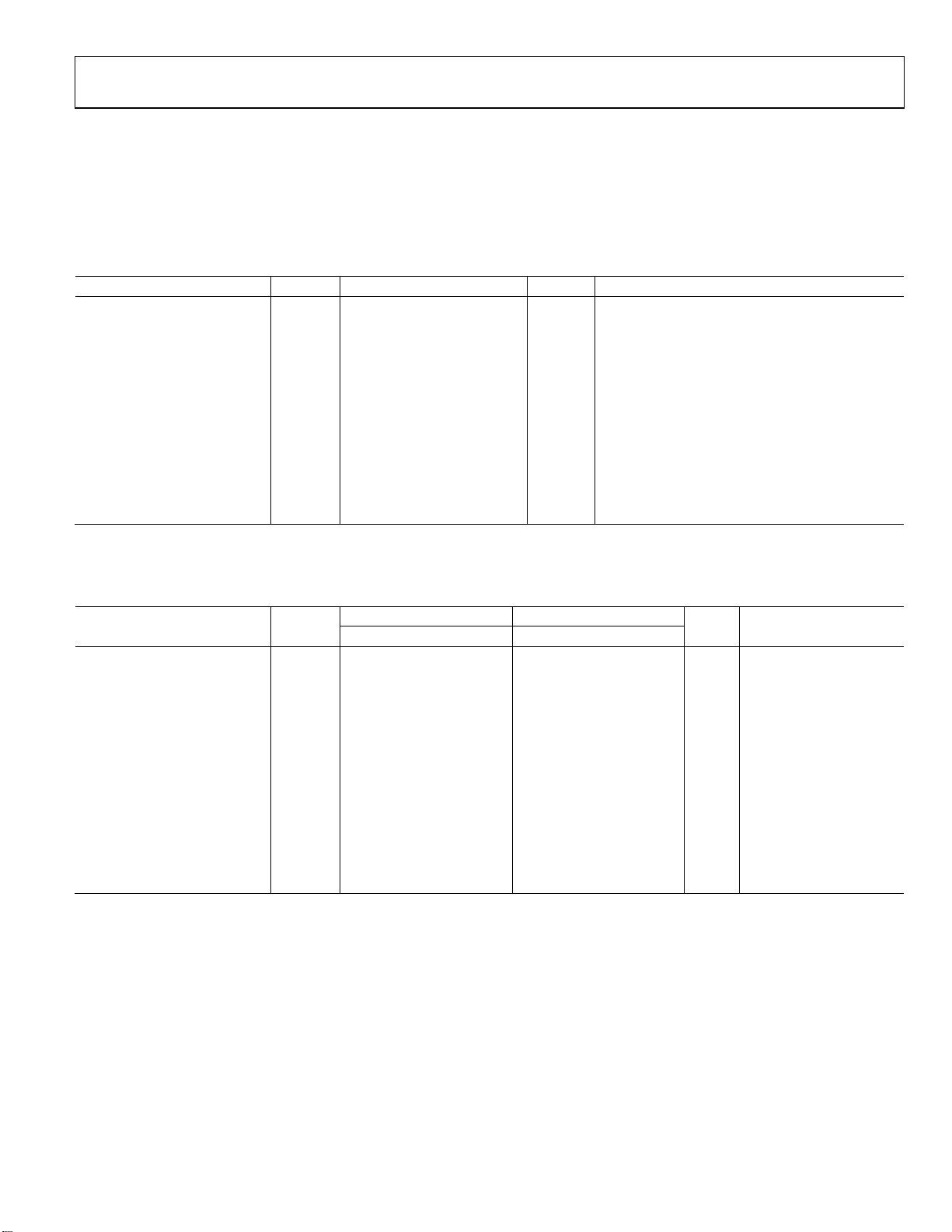
ELECTRICAL CHARACTERISTICS—5 V PRIMARY INPUT SUPPLY/5 V SECONDARY ISOLATED SUPPLY
Typical specifications are at TA = 25°C, V
operation range, which is 4.5 V ≤ V
tested with C
= 15 pF and CMOS signal levels, unless otherwise noted.
L
DD1
Table 2. DC-to-DC Converter Static Specifications
Parameter Symbol Min Typ Max Unit Test Conditions/Comments
DC-TO-DC CONVERTER SUPPLY
Setpoint V
Line Regulation V
Load Regulation V
Output Ripple V
Output Noise V
Switching Frequency f
PWM Frequency f
Output Supply Current I
Efficiency at I
I
, No V
DD1
I
DD1
, Full V
ISO
ISO
34 % I
ISO(MAX)
Load I
Load I
ISO
ISO(LINE)
ISO(LOAD)
ISO(RIP)
ISO(NOISE)
OSC
PWM
ISO(MAX)
DD1(Q)
DD1(MAX)
= V
= V
DD1
SEL
, V
, V
≤ 5.5 V, and −40°C ≤ TA ≤ +105°C, unless otherwise noted. Switching specifications are
SEL
ISO
4.7 5.0 5.4 V I
1 mV/V I
1 5 % I
= 5 V. Minimum/maximum specifications apply over the entire recommended
ISO
= 0 mA
ISO
= 40 mA, V
ISO
= 8 mA to 72 mA
ISO
= 4.5 V to 5.5 V
DD1
75 mV p-p 20 MHz bandwidth, CBO = 0.1 μF||10 μF, I
200 mV p-p CBO = 0.1 μF||10 μF, I
= 72 mA
ISO
180 MHz
625 kHz
80 mA V
> 4.5 V
ISO
= 80 mA
ISO
13 35 mA
290 mA
= 72 mA
ISO
Table 3. DC-to-DC Converter Dynamic Specifications
1 Mbps—A or C Grade 25 Mbps—C Grade
Parameter Symbol
Min Typ Max Min Typ Max
Unit
Test Conditions/
Comments
SUPPLY CURRENT
Input I
ADuM6400 12 64 mA No V
ADuM6401 12 68 mA No V
ADuM6402 13 71 mA No V
ADuM6403 14 75 mA No V
ADuM6404 14 78 mA No V
Available to Load I
ADuM6400
DD1(D)
ISO(LOAD)
80 69 mA
ISO
ISO
ISO
ISO
ISO
load
load
load
load
load
ADuM6401 80 67 mA
ADuM6402 80 65 mA
ADuM6403 80 63 mA
ADuM6404 80 61 mA
Rev. A | Page 3 of 28

ADuM6400/ADuM6401/ADuM6402/ADuM6403/ADuM6404 Data Sheet
Table 4. Switching Specifications
A Grade C Grade
Parameter Symbol
Unit
SWITCHING SPECIFICATIONS
Data Rate 1 25 Mbps Within PWD limit
Propagation Delay t
, t
55 100 45 60 ns 50% input to 50% output
PHL
PLH
Pulse Width Distortion PWD 40 6 ns |t
Change vs. Temperature 5 ps/°C
Pulse Width PW 1000 40 ns Within PWD limit
Propagation Delay Skew t
50 15 ns Between any two units
PSK
Channel Matching
Codirectional
Opposing Directional
1
7Codirectional channel matching is the absolute value of the difference in propagation delays between any two channels with inputs on the same side of the isolation
barrier.
2
Opposing directional channel matching is the absolute value of the difference in propagation delays between any two channels with inputs on opposite sides of the
isolation barrier.
1
t
2
t
50 6 ns
PSKCD
50 15 ns
PSKOD
Table 5. Input and Output Characteristics
Parameter Symbol Min Typ Max Unit
DC SPECIFICATIONS
Logic High Input Threshold VIH 0.7 × V
Logic Low Input Threshold VIL 0.3 × V
Logic High Output Voltages VOH V
V
− 0.3 or V
DD1
− 0.5 or V
DD1
or 0.7 × V
ISO
V
DD1
or 0.3 × V
ISO
− 0.3 5.0 V IOx = −20 μA, VIx = V
ISO
− 0.5 4.8 V IOx = −4 mA, VIx = V
ISO
V
DD1
Logic Low Output Voltages VOL 0.0 0.1 V IOx = 20 μA, VIx = V
0.2 0.4 V IOx = 4 mA, VIx = V
Undervoltage Lockout UVLO V
Positive-Going Threshold V
Negative-Going Threshold V
Hysteresis V
UV+
UV−
UVH
2.7 V
2.4 V
0.3 V
Input Currents per Channel II −20 +0.01 +20 μA 0 V ≤ VIx ≤ V
AC SPECIFICATIONS
Output Rise/Fall Time tR/tF 2.5 ns 10% to 90%
Common-Mode Transient
Immunity
1
|CM| 25 35 kV/μs
Refresh Rate fr 1.0 Mbps
1
|CM | is the maximum common-mode voltage slew rate that can be sustained while maintaining VO > 0.7 × V
input. The common-mode voltage slew rates apply to both rising and falling common-mode voltage edges.
or 0.7 × V
DD1
for a high input or VO < 0.3 × V
ISO
Test Conditions/
Comments Min Typ Max Min Typ Max
− t
PHL
|
PLH
Test Conditions/
Comments
IxH
IxH
IxL
IxL
, V
, V
DD1
DDL
or V
supplies
ISO
DDx
, VCM = 1000 V,
ISO
DD1
= V
V
Ix
transient magnitude = 800 V
or 0.3 × V
DD1
for a low
ISO
Rev. A | Page 4 of 28
Data Sheet ADuM6400/ADuM6401/ADuM6402/ADuM6403/ADuM6404
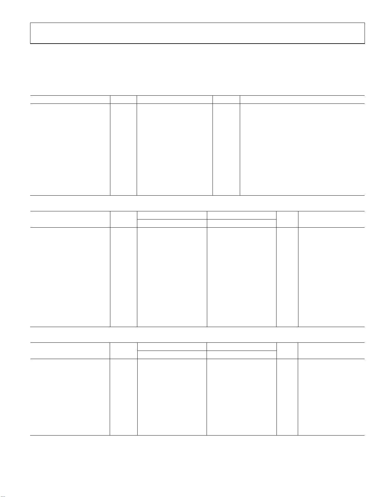
ELECTRICAL CHARACTERISTICS—3.3 V PRIMARY INPUT SUPPLY/3.3 V SECONDARY ISOLATED SUPPLY
Typical specifications are at TA = 25°C, V
recommended operation range, which is 3.0 V ≤ V
specifications are tested with C
= 15 pF and CMOS signal levels, unless otherwise noted.
L
Table 6. DC-to-DC Converter Static Specifications
Parameter Symbol Min Typ Max Unit Test Conditions/Comments
DC-TO-DC CONVERTER SUPPLY
Setpoint V
Line Regulation V
Load Regulation V
Output Ripple V
Output Noise V
Switching Frequency f
PWM Frequency f
Output Supply Current I
Efficiency at I
I
, No V
DD1
I
, Full V
DD1
ISO
ISO
33 % I
ISO(MAX)
Load I
Load I
ISO
ISO(LINE)
ISO(LOAD)
ISO(RIP)
ISO(NOISE)
OSC
PWM
ISO(MAX)
DD1(Q)
DD1(MAX)
Table 7. DC-to-DC Converter Dynamic Specifications
Parameter Symbol
SUPPLY CURRENT
Input I
DD1(D)
ADuM6400 8 41 mA No V
ADuM6401 8 44 mA No V
ADuM6402 8 46 mA No V
ADuM6403 9 47 mA No V
ADuM6404 9 51 mA No V
Available to Load I
ADuM6400
ISO(LOAD)
ADuM6401 40 31 mA
ADuM6402 40 30 mA
ADuM6403 40 29 mA
ADuM6404 40 28 mA
Table 8. Switching Specifications
Parameter Symbol
SWITCHING SPECIFICATIONS
Data Rate 1 25 Mbps Within PWD limit
Propagation Delay t
PHL
Pulse Width Distortion PWD 40 6 ns |t
Change vs. Temperature 5 ps/°C
Pulse Width PW 1000 40 ns Within PWD limit
Propagation Delay Skew t
PSK
Channel Matching
Codirectional
Opposing Directional
1
7Codirectional channel matching is the absolute value of the difference in propagation delays between any two channels with inputs on the same side of the isolation
barrier.
2
Opposing directional channel matching is the absolute value of the difference in propagation delays between any two channels with inputs on opposite sides of the
isolation barrier.
1
t
2
t
PSKCD
PSKOD
= V
DD1
= 3.3 V, V
ISO
, V
DD1
3.0 3.3 3.6 V I
1 mV/V I
1 5 % I
50 mV p-p 20 MHz bandwidth, CBO = 0.1 μF||10 μF, I
130 mV p-p CBO = 0.1 μF||10 μF, I
= GND
SEL
, V
≤ 3.6 V, and −40°C ≤ TA ≤ +105°C, unless otherwise noted. Switching
SEL
ISO
. Minimum/maximum specifications apply over the entire
ISO
= 0 mA
ISO
= 20 mA, V
ISO
= 4 mA to 36 mA
ISO
= 3.0 V to 3.6 V
DD1
= 54 mA
ISO
= 54 mA
ISO
180 MHz
625 kHz
40 mA V
> 3 V
ISO
= 40 mA
ISO
15 28 mA
175 mA
1 Mbps—A or C Grade 25 Mbps—C Grade
Unit
Test Conditions/
Comments Min Typ Max Min Typ Max
load
ISO
load
ISO
load
ISO
load
ISO
load
ISO
40 33 mA
A Grade C Grade
Unit
, t
60 100 45 65 ns 50% input to 50% output
PLH
Test Conditions/
Comments Min Typ Max Min Typ Max
− t
|
PLH
PHL
50 45 ns Between any two units
50 6 ns
50 15 ns
Rev. A | Page 5 of 28

ADuM6400/ADuM6401/ADuM6402/ADuM6403/ADuM6404 Data Sheet
Table 9. Input and Output Characteristics
Test Conditions/
Parameter Symbol Min Typ Max Unit
DC SPECIFICATIONS
Logic High Input Threshold VIH 0.7 × V
Logic Low Input Threshold VIL 0.3 × V
Logic High Output Voltages VOH V
V
− 0.2 or V
DD1
− 0.5 or V
DD1
or 0.7 × V
ISO
V
DD1
or 0.3 × V
ISO
− 0.2 3.3 V IOx = −20 μA, VIx = V
ISO
− 0.5 3.1 V IOx = −4 mA, VIx = V
ISO
V
DD1
Logic Low Output Voltages VOL 0.0 0.1 V IOx = 20 μA, VIx = V
0.0 0.4 V IOx = 4 mA, VIx = V
Undervoltage Lockout UVLO V
Positive-Going Threshold V
Negative-Going Threshold V
Hysteresis V
UV+
UV−
UVH
2.7 V
2.4 V
0.3 V
Input Currents per Channel II −10 +0.01 +10 μA 0 V ≤ VIx ≤ V
AC SPECIFICATIONS
Output Rise/Fall Time tR/tF 2.5 ns 10% to 90%
Common-Mode Transient
Immunity
1
|CM| 25 35 kV/μs
Refresh Rate fr 1.0 Mbps
1
|CM | is the maximum common-mode voltage slew rate that can be sustained while maintaining VO > 0.7 × V
input. The common-mode voltage slew rates apply to both rising and falling common-mode voltage edges.
or 0.7 × V
DD1
for a high input or VO < 0.3 × V
ISO
Comments
IxH
IxH
IxL
IxL
, V
, V
DD1
DDL
or V
supplies
ISO
DDx
, VCM = 1000 V,
ISO
DD1
= V
V
Ix
transient magnitude = 800 V
or 0.3 × V
DD1
for a low
ISO
ELECTRICAL CHARACTERISTICS—5 V PRIMARY INPUT SUPPLY/3.3 V SECONDARY ISOLATED SUPPLY
Typical specifications are at TA = 25°C, V
recommended operation range, which is 4.5 V ≤ V
Switching specifications are tested with C
Table 10. DC-to-DC Converter Static Specifications
Parameter Symbol Min Typ Max Unit Test Conditions/Comments
DC-TO-DC CONVERTER SUPPLY
Setpoint V
Line Regulation V
Load Regulation V
Output Ripple V
Output Noise V
Switching Frequency f
PWM Frequency f
Output Supply Current I
Efficiency at I
I
, No V
DD1
I
DD1
, Full V
ISO
ISO
30 % I
ISO(MAX)
Load I
Load I
ISO
ISO(LINE)
ISO(LOAD)
ISO(RIP)
ISO(NOISE)
OSC
PWM
ISO(MAX)
DD1(Q)
DD1(MAX)
= 5.0 V, V
DD1
= 15 pF and CMOS signal levels, unless otherwise noted.
L
3.0 3.3 3.6 V I
1 mV/V I
1 5 % I
= 3.3 V, V
ISO
≤ 5.5 V, 3.0 V ≤ V
DD1
= GND
SEL
. Minimum/maximum specifications apply over the entire
ISO
≤ 3.6 V, and −40°C ≤ TA ≤ +105°C, unless otherwise noted.
ISO
= 0 mA
ISO
= 50 mA, V
ISO
= 10 mA to 90 mA
ISO
= 4.5 V to 5.5 V
DD1
50 mV p-p 20 MHz bandwidth, CBO = 0.1 μF||10 μF, I
130 mV p-p CBO = 0.1 μF||10 μF, I
= 90 mA
ISO
180 MHz
625 kHz
100 mA V
> 3 V
ISO
= 100 mA
ISO
11 20 mA
230 mA
= 90 mA
ISO
Rev. A | Page 6 of 28
Data Sheet ADuM6400/ADuM6401/ADuM6402/ADuM6403/ADuM6404
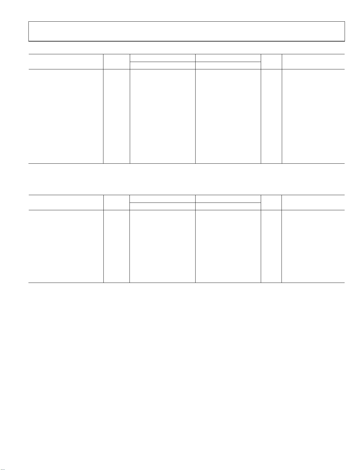
Table 11. DC-to-DC Converter Dynamic Specifications
1 Mbps—A or C Grade 25 Mbps—C Grade
Parameter Symbol
Unit
SUPPLY CURRENT
Input I
DD1(D)
ADuM6400 6 43 mA No V
ADuM6401 6 44 mA No V
ADuM6402 7 45 mA No V
ADuM6403 7 46 mA No V
ADuM6404 7 47 mA No V
Available to Load I
ADuM6400
ISO(LOAD)
100 93 mA
ADuM6401 100 92 mA
ADuM6402 100 91 mA
ADuM6403 100 89 mA
ADuM6404 100 88 mA
Table 12. Switching Specifications
A Grade C Grade
Parameter Symbol
Unit
SWITCHING SPECIFICATIONS
Data Rate 1 25 Mbps Within PWD limit
Propagation Delay t
, t
60 100 45 60 ns 50% input to 50% output
PHL
PLH
Pulse Width Distortion PWD 40 6 ns |t
Change vs. Temperature 5 ps/°C
Pulse Width PW 1000 40 ns Within PWD limit
Propagation Delay Skew t
50 15 ns Between any two units
PSK
Channel Matching
Codirectional
Opposing Directional
1
7Codirectional channel matching is the absolute value of the difference in propagation delays between any two channels with inputs on the same side of the isolation
barrier.
2
Opposing directional channel matching is the absolute value of the difference in propagation delays between any two channels with inputs on opposite sides of the
isolation barrier.
1
t
2
t
50 6 ns
PSKCD
50 15 ns
PSKOD
Test Conditions/
Comments Min Typ Max Min Typ Max
load
ISO
load
ISO
load
ISO
load
ISO
load
ISO
Test Conditions/
Comments Min Typ Max Min Typ Max
− t
|
PLH
PHL
Rev. A | Page 7 of 28
ADuM6400/ADuM6401/ADuM6402/ADuM6403/ADuM6404 Data Sheet
Table 13. Input and Output Characteristics
Parameter Symbol Min Typ Max Unit Test Conditions/Comments
DC SPECIFICATIONS
Logic High Input Threshold VIH
0.7 × V
0.7 × V
ISO
DD1
or
Logic Low Input Threshold VIL
Logic High Output Voltages VOH
V
DD1
V
ISO
V
DD1
V
ISO
− 0.2 or
− 0.2
− 0.5 or
− 0.5
Logic Low Output Voltages VOL 0.0 0.1 V IOx = 20 μA, VIx = V
0.0 0.4 V IOx = 4 mA, VIx = V
Undervoltage Lockout UVLO V
Positive-Going Threshold V
Negative-Going Threshold V
Hysteresis V
UV+
UV−
UVH
2.7 V
2.4 V
0.3 V
Input Currents per Channel II −10 +0.01 +10 μA 0 V ≤ VIx ≤ V
AC SPECIFICATIONS
Output Rise/Fall Time tR/tF 2.5 ns 10% to 90%
Common-Mode Transient
Immunity
1
|CM| 25 35 kV/μs
Refresh Rate fr 1.0 Mbps
1
|CM | is the maximum common-mode voltage slew rate that can be sustained while maintaining VO > 0.7 × V
input. The common-mode voltage slew rates apply to both rising and falling common-mode voltage edges.
V
V
for a high input or VO < 0.3 × V
ISO
V
DD1
V
DD1
V
ISO
ISO
DD1
or
0.3 × V
0.3 × V
or V
V IOx = −20 μA, VIx = V
ISO
− 0.2 or
V I
− 0.2
or 0.7 × V
DD1
IxH
= −4 mA, VIx = V
Ox
, V
, V
DD1
DDL
ISO
DDx
= V
V
or V
Ix
DD1
IxH
IxL
IxL
supplies
, VCM = 1000 V,
ISO
transient magnitude = 800 V
or 0.3 × V
DD1
for a low
ISO
PACKAGE CHARACTERISTICS
Table 14.
Parameter Symbol Min Typ Max Unit Test Conditions/Comments
RESISTANCE AND CAPACITANCE
Resistance (Input-to-Output)
Capacitance (Input-to-Output)
Input Capacitance
2
C
IC Junction-to-Ambient Thermal
Resistance
THERMAL SHUTDOWN
Thermal Shutdown Threshold TSSD 150 °C TJ rising
Thermal Shutdown Hysteresis TS
1
This device is considered a 2-terminal device; Pin 1 through Pin 8 are shorted together, and Pin 9 through Pin 16 are shorted together.
2
Input capacitance is from any input data pin to ground.
3
Refer to the section for thermal model definitions. Thermal Analysis
1
R
1
C
1012 Ω
I-O
2.2 pF f = 1 MHz
I-O
4.0 pF
I
θ
45 °C/W
JA
Thermocouple is located at the center of
the package underside; test conducted
on a 4-layer board with thin traces
20 °C
SD-HYS
3
Rev. A | Page 8 of 28
Data Sheet ADuM6400/ADuM6401/ADuM6402/ADuM6403/ADuM6404
REGULATORY INFORMATION
The ADuM6400/ADuM6401/ADuM6402/ADuM6403/ADuM6404 are approved by the organizations listed in Tabl e 15 . Refer to Ta b le 2 0
and the Insulation Lifetime section for more information about the recommended maximum working voltages for specific cross-insulation
waveforms and insulation levels.
Table 15.
1
UL
Recognized under UL 1577 component
recognition program
Single protection, 5000 V rms isolation
voltage
RW-16 package:
RI-16-1 package:
File E214100 File 205078 File 2471900-4880-0001
1
In accordance with UL 1577, each ADuM6400/ADuM6401/ADuM6402/ADuM6403/ADuM6404 is proof-tested by applying an insulation test voltage ≥ 6000 V rms for
1 sec (current leakage detection limit = 20 μA).
2
In accordance with IEC 60747-5-2 (VDE 0884 Part 2):2003-01, each ADuM6400/ADuM6401/ADuM6402/ADuM6403/ADuM6404 in the RW-16 package is proof-tested
by applying an insulation test voltage ≥ 1590 V peak for 1 sec (partial discharge detection limit = 5 pC). The asterisk (*) marking branded on the component designates
IEC 60747-5-2 (VDE 0884 Part 2):2003-01 approval.
3
In accordance with DIN V VDE V 0884-10 (VDE V 0884-10):2006-12, each ADuM6400/ADuM6401/ADuM6402/ADuM6403/ADuM6404 in the RI-16-1 package is proof-tested
by applying an insulation test voltage ≥ 1590 V peak for 1 sec (partial discharge detection limit = 5 pC). The asterisk (*) marking branded on the component designates
DIN V VDE V 0884-10 (VDE V 0884-10):2006-12 approval.
CSA (Pending) VDE
Approved under CSA Component Acceptance Notice #5A RW-16 package:
Certified according to IEC 60747-5-2
(VDE 0884 Part 2):2003-01 (pending)
Basic insulation, 846 V peak
Basic insulation per CSA 60950-1-07 and IEC 60950-1,
600 V rms (848 V peak) maximum working voltage
RI-16-1 package:
Certified according to DIN V VDE V
0884-10 (VDE V 0884-10):2006-12
Reinforced insulation, 846 V peak
Reinforced insulation per CSA 60950-1-07 and IEC 60950-1,
380 V rms (537 V peak) maximum working voltage
Reinforced insulation per IEC 60601-1, 125 V rms (176 V peak)
maximum working voltage
Reinforced insulation per CSA 60950-1-07 and IEC 60950-1,
400 V rms (565 V peak) maximum working voltage
Reinforced insulation per IEC 60601-1, 250 V rms (353 V peak)
maximum working voltage
2
3
INSULATION AND SAFETY-RELATED SPECIFICATIONS
Table 16.
Parameter Symbol Value Unit Test Conditions/Comments
Rated Dielectric Insulation Voltage 5000 V rms 1-minute duration
Minimum External Air Gap (Clearance) L(I01) 8.0 mm
Minimum External Tracking (Creepage) L(I02)
RW-16 Package 7.6 mm
RI-16-1 Package 8.3 mm
Minimum Internal Distance (Internal Clearance) 0.017 min mm Distance through insulation
Tracking Resistance (Comparative Tracking Index) CTI >175 V DIN IEC 112/VDE 0303, Part 1
Material Group IIIa Material Group (DIN VDE 0110, 1/89, Table 1)
Rev. A | Page 9 of 28
Measured from input terminals to output terminals,
shortest distance through air
Measured from input terminals to output terminals,
shortest distance path along body
 Loading...