

Page 1
FEATURES
High accuracy
Supports IEC 60687/61036 and ANSI C12.1/12.20
Suitable for class0.5 and class0.2 meter
Full four quadrant measurement of parameters
SPI® compatible serial interface
Pulse output with programmable pulse constant as
pulses/kWh or Wh/pulse
Programmable duty cycle for pulse output
Embedded calibration routines for gain and dc offset
Software based phase and nonlinearity compensation for
current transformers
15 kHz sampling frequency
UART mode enables a PC to directly access all computed
parameters
Flags to indicate tamper conditions
Single 3.0 V supply
Developer’s kit to accelerate design process (See
Ordering Guide for separate ordering number.)
GENERAL DESCRIPTION
The ADSST-SALEM-3T energy meter chipset consists of an
efficient ADSST-218x digital signal processor (DSP), a fast and
accurate 6-channel, 16-bit ADSST-73360LAR sigma-delta analog-to-digital converter (ADC), and metering software. Two
chipset versions are available to support differing ranges of
operating temperature: The ADSST-EM-3040 chipset is rated at
0°C to 70°C for commercial applications, while the ADSST-EM3041 chipset operates at –25°C to +85°C for industrial use.
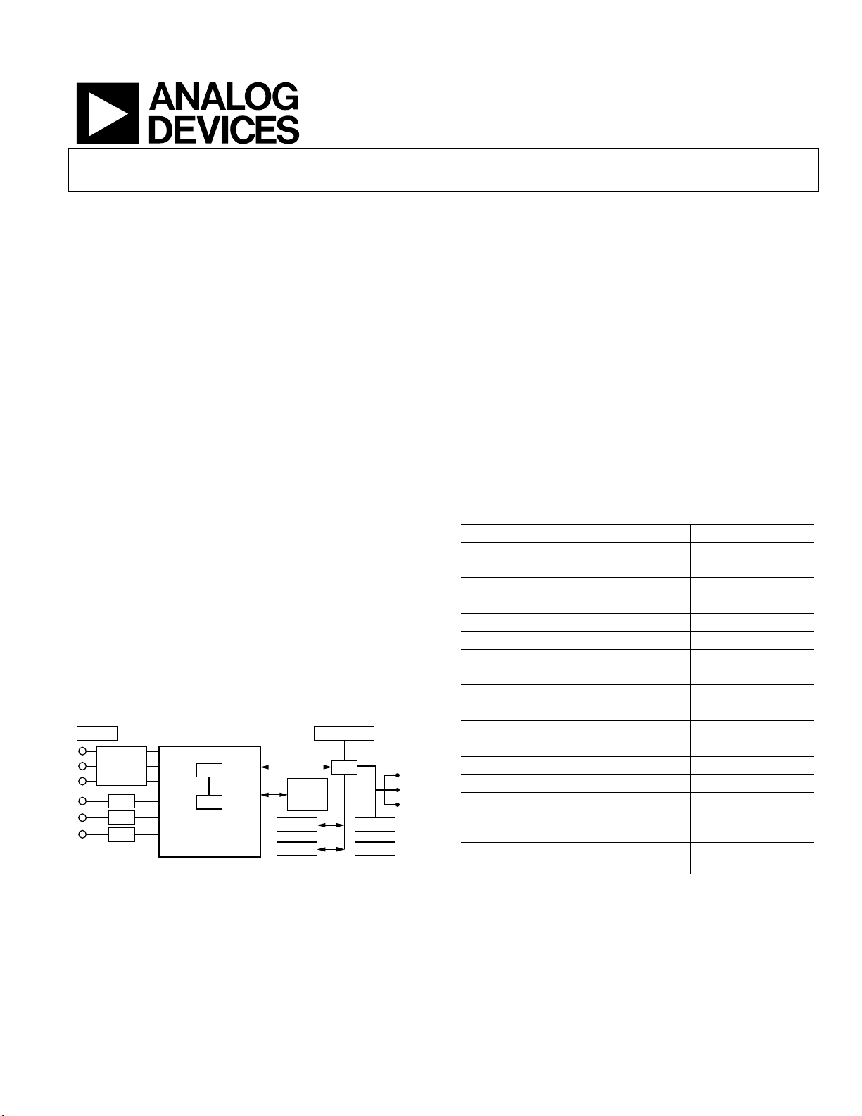
SMPS LCD DISPLAY
RESISTOR
BLOCK
CT
CT
CT
Figure 1. Block Diagram of a Functional Meter
DSP
ADC
ADSST-EM-3040
The ADC and DSP are interfaced to simultaneously acquire
voltage and current samples on all three phases and to perform
mathematically intensive computations to calculate various
instantaneous parameters and perform harmonic analysis. The
SPI BUS
BOOT
FLASH
FLASH
RTC
µC
OPTO
RS-232
03738-0-001
BUTTONS
Powerful Energy Meter Chipset
ADSST-SALEM-3T
chipset can be interfaced to any general-purpose microprocessor to develop state of the art tri-vector or polyphase energy
metering solutions with a wide range of basic currents from 1 A
to 30 A. By incorporating a comprehensive data set of parameters, including instantaneous measurements, accumulated
parameters, and harmonic analysis data, the ADSST-SALEM-3T
chipset meets high end energy metering requirements. The ability to easily configure the chipset for various parameters makes
it a very flexible solution.
The phase and nonlinearity compensation for current
transformers is done in software (patent pending) without
having to use any passive components in the circuit for
compensation, thus minimizing variations in accuracy with
temperature and time.
The ADSST-SALEM-3T measures and computes a large number of parameters essential for high end metering.
Table 1.
Parameter Each Phase Total
RMS Voltage
RMS Current
Active Power
Apparent Power
Inductive Reactive Power
Capacitive Reactive Power
Power Factor
Frequency
Positive Active Energy
Negative Active Energy
Apparent Energy
Positive Inductive Reactive Energy
Negative Inductive Reactive Energy
Positive Capacitive Reactive Energy
Negative Capacitive Reactive Energy
Voltage Magnitude and Phase for All
Odd Harmonics up to 21
Current Magnitude and Phase for All
Odd Harmonics up to 21
st
Order
st
Order
The ADSST-SALEM-3T offers some excellent features that
make the final meter cost-effective and easy to manufacture.
Rev. 0
Information furnished by Analog Devices is believed to be accurate and reliable.
However, no responsibility is assumed by Analog Devices for its use, nor for any
infringements of patents or other rights of third parties that may result from its use.
Specifications subject to change without notice. No license is granted by implication
or otherwise under any patent or patent rights of Analog Devices. Trademarks and
registered trademarks are the property of their respective owners.
One Technology Way, P.O. Box 9106, Norwood, MA 02062-9106, U.S.A.
Tel: 781.329.4700
Fax: 781.326.8703 © 2004 Analog Devices, Inc. All rights reserved.
www.analog.com
Page 2

ADSST-SALEM-3T
TABLE OF CONTENTS
Easy Calibration............................................................................ 3
Effective Phase Compensation ................................................... 3
Ease of Design............................................................................... 3
Quadrant and Other Conventions ............................................. 3
General Description of the ADSST-218x DSP ......................... 4
General Description of the ADSST-73360LAR ADC................ 11
Specifications—ADSST-73360LAR ............................................. 12
Absolute Maximum Ratings—ADSST-73360LAR .................... 14
ESD Caution................................................................................ 14
Pin Configuration and Pin Function Descriptions—
ADSST-73360LAR
.......................................................................... 15
Architecture Overview ................................................................ 4
ADSST-218x Common-Mode Pins ........................................... 6
Clock Signals................................................................................. 7
............................................................................................ 7
RESET
Recommended Operating Conditions ...................................... 7
ADSST-218x Electrical Characteristics ......................................... 8
Absolute Maximum Ratings—ADSST-218x................................. 9
ESD Caution.................................................................................. 9
Pin Configuration—ADSST-218x................................................ 10
REVISION HISTORY
7/04—Revision 0: Initial Version
Pin Function Descriptions ........................................................ 15
Grounding and Layout .............................................................. 16
Power-Up Initialization and Data from the
ADSST-SALEM-3T
Voltage and Current Sensing .................................................... 17
Accuracy of Reference Design Using the
ADSST-SALEM-3T Chipset
Outline Dimensions....................................................................... 20
Ordering Guide............................................................................... 21
.................................................................... 17
..................................................... 18
Rev. 0 | Page 2 of 24
Page 3
ADSST-SALEM-3T
EASY CALIBRATION
The ADSST-SALEM-3T chipset has highly advanced calibration
routines embedded into the software. Ease of calibration is the
key feature in this chipset. By sending specific commands to the
ADSST-SALEM-3T chipset, the dc offsets and gains for all voltage and current channels can be calibrated automatically. Active
and reactive power calibration is also available for fine-tuning
the errors.
The meter and calibration constants are stored in an external
flash memory, and the lock/unlock calibration feature enables
protection of the calibration constants. The ability to upgrade
the firmware residing in the flash memory makes the meter
adaptable to future needs.
EFFECTIVE PHASE COMPENSATION
The ADSST-SALEM-3T chipset employs an algorithm (patent
pending) for phase compensation. The ADSST-SALEM3T chipset based meter, which is very effective and user friendly,
can be calibrated for phase compensation at three current
points to cover the complete current range. This also reduces
the cost of the end product by reducing the cost of the sensing
elements, i.e., current transformers.
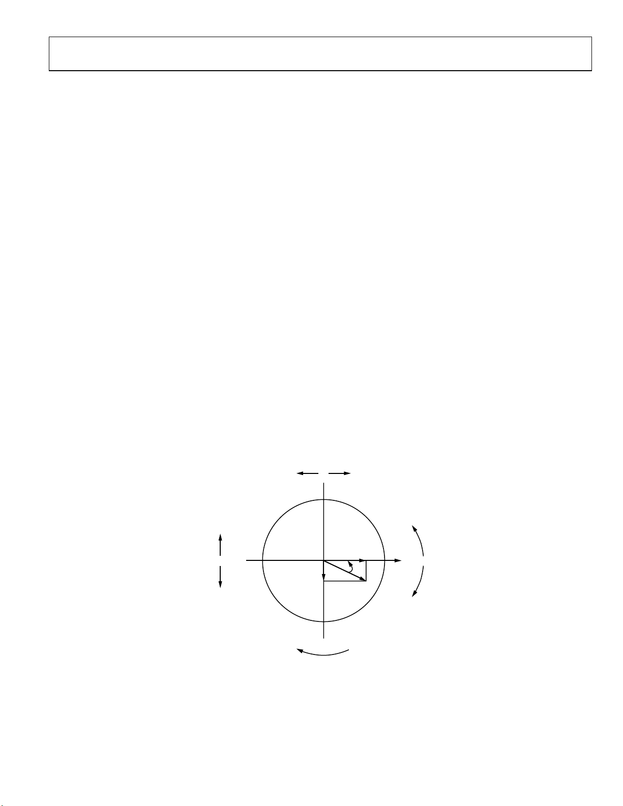
ACTIVE EXPORT
REACTIVE
SIN Φ =–1
EASE OF DESIGN
Designing a complete meter using the ADSST-SALEM-3T is
very easy with the ADSST-SALEM-3T-DK developer’s kit. The
kit in the UART mode enables a user to evaluate and test the
computational element by connecting to a PC, without building
the complete hardware.
QUADRANT AND OTHER CONVENTIONS
The metering data computed by the ADSST-SALEM-3T chipset
uses the following conventions for various parameters:
• Figure 2 gives the quadrant conventions used by the
chipset.
• Import means power delivered from the utility to the user.
• Export means power delivered by the user to the utility.
• Total means total of all three phases.
Import and export are with reference to consumption.
U, I: Magnitude of voltage and current
P: Active Power (U × I × cos Φ)
Q: Reactive Power (U × I × sin Φ)
Φ: Phase angle from the standpoint of I with respect to U,
always positive in counterclockwise direction.
Phase U: L1 = 0° Abs
L2 = 240° Abs
L3 = 120° Abs
ACTIVE IMPORT
(–90° Φ)
(90° ABS)
REACTIVE EXPORT
ACTIVE
COS Φ =–1
(±180° Φ)
(180° ABS)
REACTIVE IMPORT
P–Q– P+Q–
QUADRANT II QUADRANT I
Φ
I
I
Q
QUADRANT III QUADRANT IV
P+Q+
P–Q+
REACTIVE
SIN Φ =+1
Figure 2. Quadrant Conventions
Rev. 0 | Page 3 of 24
(+90° Φ)
(270° ABS)
L1, L2, L3
ACTIVE
CAPACITIVE (LEAD)
ACTIVE
COS Φ = +1
(0° Φ)
(0° ABS)
ACTIVE
INDUCTIVE (LAG)
03738-0-002
Page 4
ADSST-SALEM-3T
GENERAL DESCRIPTION OF THE ADSST-218X DSP
The ADSST-218x is a single-chip microcomputer optimized for
digital signal processing (DSP) and other high speed numeric
processing applications.
The DSP combines the ADSP-2100 family base architecture
(three computational units, data address generators, and a program sequencer) with two serial ports, a 16-bit internal DMA
port, a byte DMA port, a programmable timer, flag I/O, extensive interrupt capabilities, and on-chip program and data
memory.
The ADSST-218x is fabricated in a high speed, low power
CMOS process. Every instruction can execute in a single processor cycle.
The ADSST-218x’s flexible architecture and comprehensive
instruction set enable the processor to perform multiple operations in parallel. In one processor cycle, the ADSST-218x can:
• Generate the next program address
• Fetch the next instruction
• Perform one or two data moves
• Update one or two data address pointers
This takes place while the processor continues to:
• Receive and transmit data through the two serial ports
• Receive and/or transmit data through the internal
DMA port
• Receive and/or transmit data through the byte DMA port
• Decrement timer
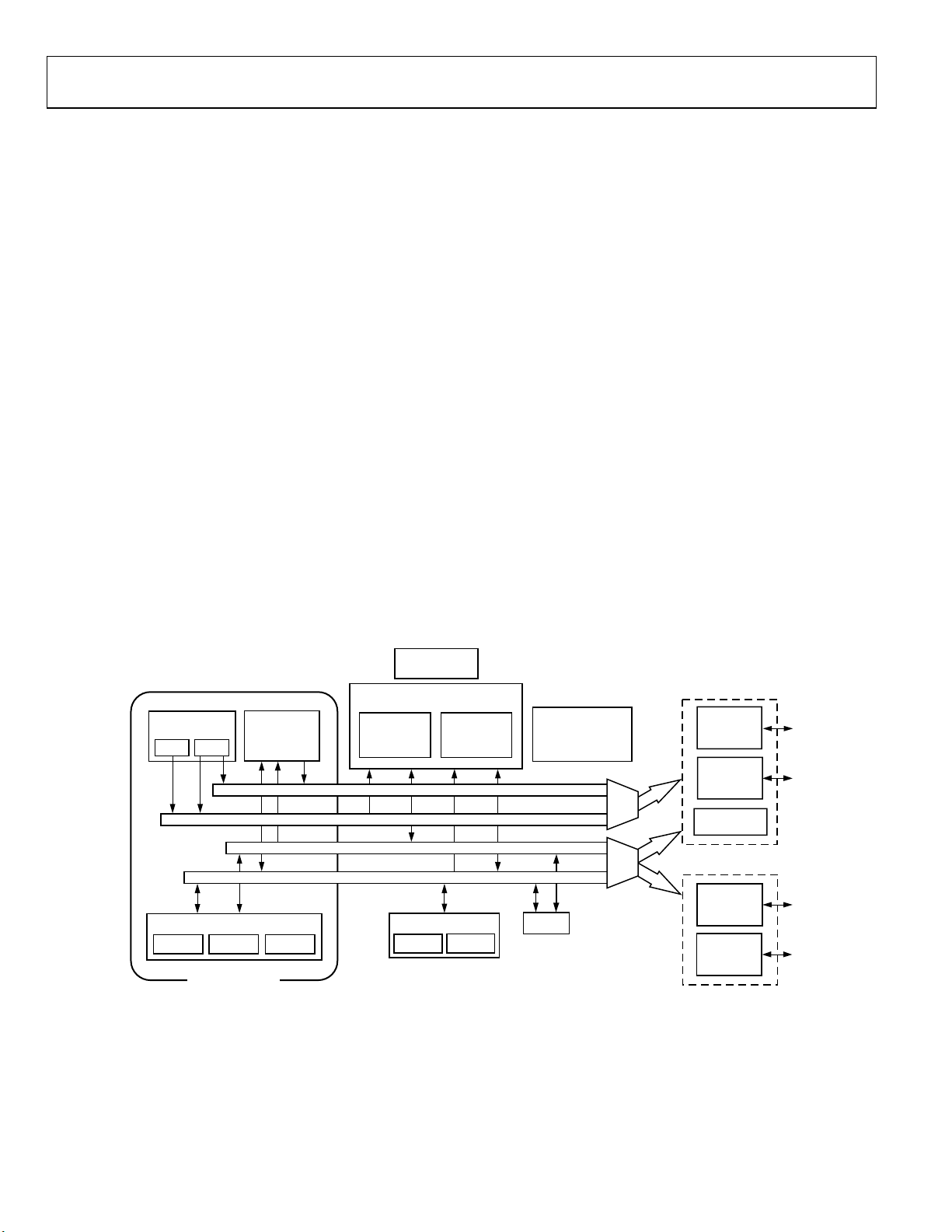
ARCHITECTURE OVERVIEW
The ADSST-218x instruction set provides flexible data moves
and multifunction (one or two data moves with a computation)
instructions. Every instruction can be executed in a single processor cycle. The ADSST-218x assembly language uses an
algebraic syntax for ease of coding and readability. A comprehensive set of development tools supports program
development.
Figure 3 is the functional block diagram of the ADSST-218x.
The processor contains three independent computational units:
the ALU, the multiplier/accumulator (MAC), and the shifter.
The computational units process 16-bit data directly and have
provisions to support multiprecision computations.
• Perform a computational operation
DATA ADDRESS
GENERATORS
DAG1 DAG2
ARITHMETIC UNITS SERIAL PORTS
ALU MAC SHIFTER
ADSP-2100 BASE
ARCHITECTURE
PROGRAM
SEQUENCER
POWER-DOWN
CONTROL
MEMORY
PROGRAM
MEMORY
16K × 24-BIT
PROGRAM MEMORY ADDRESS
DATA MEMORY ADDRESS
PROGRAM MEMORY DATA
DATA MEMORY DATA
SPORT0
MEMORY
16K × 16-BIT
SPORT1
Figure 3. Functional Block Diagram
DATA
PROGRAMMABLE
I/O
AND
FLAGS
TIMER
FULL MEMORY MODE
EXTERNAL
ADDRESS
BUS
EXTERNAL
DATA
BUS
BYTE DMA
CONTROLLER
OR
EXTERNAL
DATA
BUS
INTERNAL
DMA
PORT
HOST MODE
03738-0-008
Rev. 0 | Page 4 of 24
Page 5

ADSST-SALEM-3T
Efficient data transfer is achieved with the use of five internal
buses:
• Program Memory Address (PMA) Bus Program Memory
Data (PMD) Bus
• Data Memory Address (DMA) Bus
• Data Memory Data (DMD) Bus
• Result (R) Bus
The byte memory and I/O memory space interface supports
slow memories and I/O memory-mapped peripherals with programmable wait state generation. External devices can gain
BR
control of external buses with bus request/grant signals (
BGH
ADSST-218x to continue running from on-chip memory. Normal execution mode requires the processor to halt while buses
are granted.
, and
BG0
). One execution mode (go mode) enables the
,
The ADSST-218x can respond to 11 interrupts. There are up to
six external interrupts (one edge sensitive, two level sensitive,
and three configurable) and seven internal interrupts generated
by the timer, the serial ports (SPORTs), the byte DMA port, and
RESET
the power-down circuitry. There is also a master
The two serial ports provide a complete synchronous serial
interface with optional companding in hardware and a wide
variety of framed or frameless data transmit and receive modes
of operation.
signal.
Serial Ports
The ADSST-218x incorporates two complete synchronous serial
ports (SPORT0 and SPORT1) for serial communications and
multiprocessor communication.
Package Description
The ADSST-218x is available in a 100-lead low profile quad flat
package (LQFP, refer to Figure 5).
Rev. 0 | Page 5 of 24
Page 6
ADSST-SALEM-3T
ADSST-218X COMMON-MODE PINS
Table 2.
Pin Name No. of Pins I/O Function
BG
BGH
BMS
BR
CMS
DMS
IOMS
PMS
RD
RESET
WR
IRQ2/
PF7 I/O Programmable I/O Pin
IRQL1/
PF6 I/O Programmable I/O Pin
IRQL0/
PF5 I/O Programmable I/O Pin
IRQE/
PF4 I/O Programmable I/O Pin
MODE A 1 I
PF0 I/O Programmable I/O Pin during Normal Operation
MODE B 1 I
PF1 I/O Programmable I/O Pin during Normal Operation
MODE C 1 I
PF2 I/O Programmable I/O Pin during Normal Operation
MODE D 1 I
PF3 I/O Programmable I/O Pin during Normal Operation
CLKIN, XTAL 2 I Clock or Quartz Crystal Input
CLKOUT 1 O Processor Clock Output
EZ-Port 9 I/O For Emulation Use
FI, FO Flag In, Flag Out
FL0, FL1, FL2 3 O Output Flags
GND 10 I Power and Ground
IRQ1:0
PWD
SPORT0 5 I/O Serial Port I/O Pins
SPORT1 5 I/O Serial Port I/O Pins
PWDACK 1 O Power-Down Control Output
V
DDEXT
V
DDEXT
V
2 I Internal VDD (2.5 V) Power (LQFP)
DDINT
V
4 I Internal VDD (2.5 V) Power (Mini-BGA)
DDINT
1
Interrupt/flag pins retain both functions concurrently. If IMASK is set to enable the corresponding interrupts, the DSP will vector to the appropriate interrupt vector
address when the pin is asserted, either by external devices or set as a programmable flag.
2
SPORT configuration determined by the DSP System Control register. Software configurable.
1 O Bus Grant Output
1 O Bus Grant Hung Output
1 O Byte Memory Select Output
1 I Bus Request Input
1 O Combined Memory Select Output
1 O Data Memory Select Output
1 O Memory Select Output
1 O Program Memory Select Output
1 O Memory Read Enable Output
1 I Processor Reset Input
1 O Memory Write Enable Output
1 I Edge- or Level-Sensitive Interrupt Request
1 I Level-Sensitive Interrupt Requests
1 I Level-Sensitive Interrupt Requests
1 I Edge-Sensitive Interrupt Requests
1
1
1
Mode Select Input−Checked only during RESET
Mode Select Input−Checked only during RESET
Mode Select Input−Checked only during RESET
Mode Select Input−Checked only during RESET
2
Edge- or Level-Sensitive Interrupts
1 I Power-Down Control Input
4
7
I External VDD (2.5 V or 3.3 V) Power (LQFP)
I External V
(2.5 V or 3.3 V) Power (Mini-BGA)
DD
1
Rev. 0 | Page 6 of 24
Page 7
ADSST-SALEM-3T
CLOCK SIGNALS
Either a crystal or a TTL compatible clock signal can clock the
ADSST-218x.
If an external clock is used, it should be a TTL compatible signal
running at half the instruction rate. The signal is connected to
the processor’s CLKIN input. When an external clock is used,
the XTAL input must be left unconnected.
RESET
The
The
sequence to assure proper initialization.
power-up must be held long enough to enable the internal clock
to stabilize. If
clock continues to run and does not require stabilization time.
signal initiates a master reset of the ADSST-2185x.
RESET
signal must be asserted during the power-up
RESET
RESET
is activated any time after power-up, the
RESET
during initial
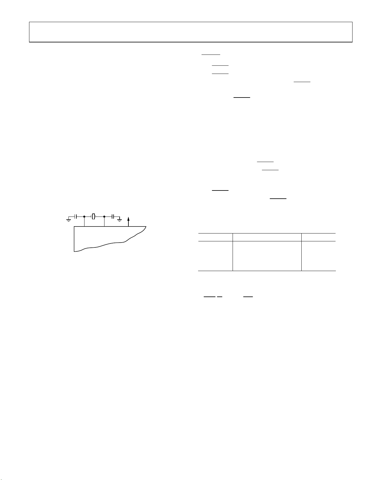
Because the ADSST-218x includes an on-chip oscillator circuit,
an external crystal may be used. The crystal should be
connected across the CLKIN and XTAL pins, with two
capacitors connected as shown in Figure 4. The capacitor values
are dependent on the crystal type and should be specified by the
crystal manufacturer. A parallel resonant, fundamental
frequency, microprocessor grade crystal should be used.
A clock output (CLKOUT) signal is generated by the processor
at the processor’s cycle rate. This can be enabled and disabled by
the CLKODIS bit in the SPORT0 autobuffer control register.
CLKIN XTAL
DSP
Figure 4. External Crystal Connections
CLKOUT
03738-0-003
The power-up sequence is defined as the total time required for
the crystal oscillator circuit to stabilize after a valid V
DD
is
applied to the processor and for the internal phase-locked loop
(PLL) to lock onto the specific crystal frequency. A minimum of
2000 CLKIN cycles ensures that the PLL has locked but does
not include the crystal oscillator start-up time. During this
power-up sequence, the
any subsequent resets, the
minimum pulse-width specification, t
The
input contains some hysteresis; however, if an RC
RESET
circuit is used to generate the
signal should be held low. On
RESET
signal must meet the
RESET
.
RSP
signal, the use of an exter-
RESET
nal Schmitt trigger is recommended.
RECOMMENDED OPERATING CONDITIONS
Table 3.
Parameter Min Max Unit
V
DDINT
V
DDEXT
1
V
INPUT
T
AMB
1
The ADSST-2185x is 3.3 V tolerant (always accepts up to 3.6 V max VIH), but
voltage compliance (on output, V
(MAX) = V
V
OH
RFS1, SCLK0, SCLK1, TFS0, A1–A13, PF0–PF7) and input only pins (CLKIN,
RESET
, BR, DR0, DR1,
2.37 2.63 V
2.37 3.60 V
VIL = –0.3 VIH = 3.6 V
0 70 °C
) depends on the input V
(MAX). This applies to bidirectional pins (D0–D23, RFS0,
DDEXT
PWD
OH
).
DDEXT
; because
Rev. 0 | Page 7 of 24
Page 8
ADSST-SALEM-3T
ADSST-218X ELECTRICAL CHARACTERISTICS
Table 4.
Parameter Test Conditions Min Typ Max Unit
VIH High Level Input Voltage
VIH High Level CLKIN Voltage @ V
VIL Low Level Input Voltage
VOH High Level Output Voltage
@ V
@ V
VOL Low Level Output Voltage
IIH High Level Input Current
IIL Low Level Input Current
I
Three-State Leakage Current
OZH
I
Three-State Leakage Current
OZL
IDD Supply Current (Idle)
@ V
IDD Supply Current (Dynamic)
@ V
IDD Supply Current (Power-Down)
CI Input Pin Capacitance
CO Output Pin Capacitance
1
Bidirectional pins: D0–D23, RFS0, RFS1, SCLK0, SCLK1, TFS0, TFS1, A1–A13, PF0–PF7.
2
Input only pins:
3
Input only pins: CLKIN,
4
Output pins: BG,
5
Although specified for TTL outputs, all ADSP-2186 outputs are CMOS compatible and will drive to V
6
Guaranteed but not tested.
7
Three-statable pins: A0–A13, D0–D23,
8
0 V on BR.
9
Idle refers to ADSST-218x state of operation during execution of IDLE instruction. Deasserted pins are driven to either VDD or GND.
10
IDD measurement taken with all instructions executing from internal memory. 50% of the instructions are multifunction (Types 1, 4, 5, 12, 13, 14), 30% are Type 2 and
Type 6, and 20% are idle instructions.
11
VIN = 0 V and 3 V. For typical figures for supply currents, refer to the Power Dissipation section.
12
Applies to LQFP package type.
13
Output pin capacitance is the capacitive load for any three-stated output pin.
RESET, BR
RESET, BR
PMS, DMS, BMS, IOMS, CMS, RD, WR
1, 2
1, 3
3
3
9
10
3, 6
6, 7, 12, 13
, DR0, DR1,
, DR0, DR1,
@ V
= Max 1.5 V
DDINT
= Max 2.0 V
DDINT
@ V
= Min 0.7 V
1, 4, 5
1, 4, 5
7
7
12
DDINT
@ V
= Min, IOH = –0.5 mA 2.0 V
DDEXT
= 3.0 V, IOH = –0.5 mA 2.4 V
DDEXT
= Min, IOH = –100 µA
DDEXT
@ V
= Min, IOL = 2 mA 0.4 V
DDEXT
@ V
= Max, VIN = 3.6 V 10 µA
DDINT
@ V
= Max, VIN = 0 V 10 µA
DDINT
@ V
= Max, VIN = 3.6 V
DDEXT
@ V
= Max, VIN = 0 V
DDEXT
@ V
= 2.5 V, tCK = 15 ns 9 mA
DDINT
= 2.5 V, tCK = 13.3 ns 10 mA
DDINT
@ V
= 2.5 V, tCK = 13.3 ns11, T
DDINT
= 2.5 V, tCK = 15 ns11, T
DDINT
@ V
= 2.5 V, T
DDINT
@ VIN = 2.5 V, fIN = 1.0 MHz, T
@ VIN = 2.5 V, fIN = 1.0 MHz, T
PWD
.
PWD
.
, PWDACK, A0, DT0, DT1, CLKOUT, FL2–0,
PMS, DMS, BMS, IOMS, CMS, RD, WR
6
8
8
= +25°C 35 mA
AMB
= +25°C 38 mA
AMB
= +25°C in Lowest Power Mode 100 mA
AMB
= +25°C 8 pF
AMB
= +25°C 8 pF
AMB
BGH
.
and GND, assuming no dc loads.
DDEXT
V
– 0.3 V
DDEXT
10 µA
10 µA
, DT0, DT1, SCLK0, SCLK1, TFS0, TFS1, RFS0, RFS1, PF0–PF7.
Rev. 0 | Page 8 of 24
Page 9

ADSST-SALEM-3T
ABSOLUTE MAXIMUM RATINGS—ADSST-218X
Table 5.
Rating
Parameter Min Max
Internal Supply Voltage (V
External Supply Voltage (V
Input Voltage
1
Output Voltage Swing
Operating Temperature Range 0°C 70°C
Storage Temperature Range –65°C +150°C
1
Applies to bidirectional pins (D0–D23, RFS0, RFS1, SCLK0, SCLK1, TFS0, TFS1,
A1–A13, PF0–PF7) and input-only pins (CLKIN,
2
Applies to output pins (BG,
A0, DT0, DT1, CLKOUT, FL2–FL0,
Stresses above those listed under Absolute Maximum Ratings
may cause permanent damage to the device. These are stress
ratings only; functional operation of the device at these or any
other conditions above those indicated in the operational sections of this specification is not implied. Exposure to absolute
maximum rating conditions for extended periods may affect
device reliability.
) –0.3 V +3.0 V
DDINT
) –0.3 V +4.0 V
DDEXT
–0.3 V +4.0 V
2
PMS, DMS, BMS, IOMS, CMS, RD, WR
–0.5 V V
BGH
).
RESET
, BR, DR0, DR1,
+ 0.5 V
DDEXT
PWD
, PWDACK,
).
ESD CAUTION
ESD (electrostatic discharge) sensitive device. Electrostatic charges as high as 4000 V readily accumulate on the
human body and test equipment and can discharge without detection. Although this product features
proprietary ESD protection circuitry, permanent damage may occur on devices subjected to high energy
electrostatic discharges. Therefore, proper ESD precautions are recommended to avoid performance
degradation or loss of functionality.
Rev. 0 | Page 9 of 24
Page 10

ADSST-SALEM-3T
A
A
A
PIN CONFIGURATION—ADSST-218X
A4/IAD3
A5/IAD4
GND
A6/IAD5
A7/IAD6
A8/IAD7
A9/IAD8
A10/IAD9
11/IAD10
12/IAD11
13/IAD12
GND
CLKIN
XTAL
V
DDEXT
CLKOUT
GND
V
DDINT
WR
RD
BMS
DMS
PMS
IOMS
CMS
A0
A1/IAD0
A3/IAD2
A2/IAD1
999897
100
1
PIN 1
2
IDENTIFIER
3
4
5
6
7
8
9
10
11
12
13
14
15
16
17
18
19
20
21
22
23
24
25
272829
26
GND
IRQE+PF4
IRQL0+PF5
IRQL1+PF6
BGH
PWDACK
96
30
IRQ2+PF7
95
31
DT0
PF0 [MODE A]
PF1 [MODE B]
9493929190
323334
TFS0
RFS0
DDEXT
V
PWD
GND
ADSST-218x
TOP VIEW
(Not to Scale)
35
36
DR0
DDEXT
SCLK0
V
FL0
PF3 [MODE D]
FL1
PF2 [MODE C]
8988878685
3738394041
DT1/FO
FL2
DR1/FI
TFS1/IRQ1
RFS1/IRQ0
D22
D23
8483828180
424344
GND
SCLK1
ERESET
D21
RESET
D18
GND
46
EE
D19
797877
48
47
ECLK
ELOUT
D17
49
ELIN
D16
76
75
D15
74
D14
73
D13
72
D12
71
GND
70
D11
69
D10
68
D9
V
67
DDEXT
66
GND
65
D8
D7/IWR
64
63
D6/IRD
62
D5/IAL
61
D4/IS
60
GND
V
59
DDINT
D3/IACK
58
D2/IAD15
57
D1/IAD14
56
55
D0/IAD13
54
BG
53
EBG
52
BR
51
EBR
50
EINT
03738-0-009
D20
45
EMS
Figure 5. Pin Configuration for ADSST-218x in 100-Lead LQFP
Rev. 0 | Page 10 of 24
Page 11

ADSST-SALEM-3T
GENERAL DESCRIPTION OF THE ADSST-73360LAR ADC
The ADSST-73360LAR is a 6-channel input analog front end
processor for general-purpose applications, including industrial
power metering or multichannel analog inputs. It features six
16-bit A/D conversion channels, each of which provides 76 dB
signal-to-noise ratio over a dc to 4 kHz signal bandwidth. Each
channel also features an input programmable gain amplifier
(PGA) with gain settings in eight stages from 0 dB to 38 dB.
VINP1
VINN1
VINP2
VINN2
VINP3
VINN3
REFCAP
REFOUT
VINP4
VINN4
SIGNAL
CONDITIONING
SIGNAL
CONDITIONING
SIGNAL
CONDITIONING
SIGNAL
CONDITIONING
0/38DB
PGA
0/38DB
PGA
0/38DB
PGA
REFERENCE
0/38DB
PGA
CONDITIONING
CONDITIONING
CONDITIONING
CONDITIONING
The ADSST-73360LAR is particularly suitable for industrial
power metering as each channel samples synchronously, ensuring that there is no (phase) delay between the conversions. The
ADSST-73360LAR also features low group delay conversions on
all channels.
An on-chip reference voltage is included with a nominal value
of 1.2 V.
The ADSST-73360LAR is available in a 28-lead SOIC package.
SIGNAL
Σ-∆
SIGNAL
Σ-∆
SIGNAL
Σ-∆
ADSST-73360LAR
SIGNAL
Σ-∆
DECIMATOR
DECIMATOR
DECIMATOR
DECIMATOR
SERIAL
I/O
PORT
SDI
SDIFS
SCLK
RESET
MCLK
SE
VINP5
VINN5
VINP6
VINN6
SIGNAL
CONDITIONING
SIGNAL
CONDITIONING
0/38DB
PGA
0/38DB
PGA
SIGNAL
Σ-∆
CONDITIONING
SIGNAL
Σ-∆
CONDITIONING
DECIMATOR
DECIMATOR
03738-0-004
SDO
SDOFS
Figure 6. ADSST-73360LAR Functional Block Diagram
Rev. 0 | Page 11 of 24
Page 12

ADSST-SALEM-3T
SPECIFICATIONS—ADSST-73360LAR
(AVDD = 2.7 V to 3.6 V, DVDD = 2.7 V to 3.6 V, DGND = AGND = 0 V, f
1
, unless otherwise noted.)
T
MAX
Table 6.
Parameter Min Typ Max Unit Test Conditions
REFERENCE
REFCAP
Absolute Voltage, V
REFCAP
1.08 1.2 1.32 V
REFCAP TC 50 ppm/°C
REFOUT
Typical Output Impedance 130 Ω
Absolute Voltage, V
REFOUT
1.08 1.2 1.32 V Unloaded
Minimum Load Resistance 1 kΩ
Maximum Load Capacitance 100 pF
ADC SPECIFICATIONS
Maximum Input Range at VIN
2, 3
1.578 V p-p Measured Differentially
–2.85 dBm
Nominal Reference Level at VIN
1.0954 V p-p Measured Differentially
(0 dBm0)
–6.02 dBm
Absolute Gain
PGA = 0 dB –1.3 +0.6 dB 1.0 kHz
PGA = 38 dB
–0.8
+0.8 dB 1.0 kHz
Signal to (Noise + Distortion)
PGA = 0 dB 76 dB 0 Hz to 4 kHz; fS = 8 kHz
PGA = 0 dB 71 76 dB 0 Hz to 2 kHz; fS = 8 kHz
f
PGA = 38 dB 58 dB 0 Hz to 4 kHz; fS = 64 kHz
Total Harmonic Distortion
PGA = 0 dB –80 –71 dB 0 Hz to 2 kHz; fS = 8 kHz; fIN = 60 kHz
PGA = 38 dB –64 dB 0 Hz to 2 kHz; fS = 64 kHz; fIN = 60 kHz
Intermodulation Distortion –78 dB PGA = 0 dB
Idle Channel Noise –68 dB PGA = 0 dB, fS = 64 kHz; SCLK = 16 MHz
Crosstalk ADC-to-ADC –95 dB ADC1 at Idle; ADC2 to ADC6 Input Signal: 60 Hz
DC Offset –30 +30 mV PGA = 0 dB
Power Supply Rejection –55 dB
Group Delay
4, 5
25
50
95
190
Input Resistance at VIN
2, 4
25 kΩ
Phase Mismatch 0.15 Degrees fIN = 1 kHz
0.01 Degrees fIN = 60 Hz
= 16.384 MHz, f
MCLK
µs
µs
µs
µs
6
= 8.192 MHz, fS = 8 kHz, TA = T
SCLK
MIN
to
0.1 µF Capacitor Required from REFCAP to AGND2
= 60 kHz
IN
Input Signal Level at AVDD and DVDD Pins
1.0 kHz, 100 mV p-p Sine Wave
64 kHz Output Sample Rate
32 kHz Output Sample Rate
16 kHz Output Sample Rate
8 kHz Output Sample Rate
DMCLK = 16.384 MHz
Rev. 0 | Page 12 of 24
Page 13

ADSST-SALEM-3T
Parameter Min Typ Max Unit Test Conditions
FREQUENCY RESPONSE
(ADC)7 Typical Output Frequency
(Normalized to f
)
S
0 0 dB
0.03125 –0.1 dB
0.0625 –0.25 dB
0.125 –0.6 dB
0.1875 –1.4 dB
0.25 –2.8 dB
0.3125 –4.5 dB
0.375 –7.0 dB
0.4375 –9.5 dB
> 0.5 < –12.5 dB
LOGIC INPUTS
V
, Input High Voltage VDD – 0.8 V
INH
V
, Input Low Voltage 0 0.8 V
INL
IIH, Input Current 10
CIN, Input Capacitance 10 pF
LOGIC OUTPUT
VOH, Output High Voltage VDD – 0.4 V
VOL, Output Low Voltage 0 0.4 V
Three-State Leakage Current –10 +10
POWER SUPPLIES
AVDD1, AVDD2 2.7 3.6 V
DVDD 2.7 3.6 V
8
IDD
1
Operating temperature range is as follows: –40°C to +85°C. Therefore, T
2
Test conditions: Input PGA set for 0 dB gain (unless otherwise noted).
3
At input to sigma-delta modulator of ADC.
4
Guaranteed by design.
5
Overall group delay will be affected by the sample rate and the external digital filtering.
6
The ADC’s input impedance is inversely proportional to DMCLK and is approximated by: (4 × 10¹¹)/DMCLK.
7
Frequency response of the ADC measured with input at audio reference level (the input level that produces an output level of 0 dBm0), with 38 dB preamplifier
bypassed and input gain of 0 dB.
8
Test Conditions: no load on digital inputs, analog inputs ac-coupled to ground.
V
DD
µA
V
DD
µA
| ≤ 100 µA
|I
OUT
| ≤ 100 µA
|I
OUT
See Table 7
= –40°C and T
MIN
= +85°C.
MAX
Table 7. Current Summary (AVDD = DVDD = 3.3 V)
Digital Current,
Conditions
Max (mA)
SE MCLK ON Comments
ADCs Only On 25 1 Yes REFOUT Disabled
REFCAP Only On 1.0 0 No REFOUT Disabled
REFCAP and REFOUT Only On 3.5 0 No
All Sections On 26.5 1 Yes REFOUT Enabled
All Sections Off 1.0 1 Yes MCLK Active Levels Equal to 0 V and DVDD
All Sections Off 0.05 0 No Digital Inputs Static and Equal to 0 V or DVDD
The above values are in mA and are typical values, unless otherwise noted. MCLK = 16.384 MHz; SCLK = 16.384 MHz.
Rev. 0 | Page 13 of 24
Page 14

ADSST-SALEM-3T
ABSOLUTE MAXIMUM RATINGS—ADSST-73360LAR
(TA = 25°C unless otherwise noted)
Table 8.
Parameter Rating
AVDD, DVDD to GND –0.3 V to +4.6 V
AGND to DGND –0.3 V to +0.3 V
Digital I/O Voltage to DGND –0.3 V to DVDD + 0.3 V
Analog I/O Voltage to AGND –0.3 V to AVDD
Operating Temperature Range 0°C to +70°C
Storage Temperature Range –65°C to +150°C
Maximum Junction Temperature 150°C
Thermal Impedance θJA (SOIC) 75°C/W
Stresses above those listed under Absolute Maximum Ratings
may cause permanent damage to the device. This is a stress
rating only; functional operation of the device at these or any
other conditions above those listed in the operational sections
of this specification is not implied. Exposure to absolute
maximum rating conditions for extended periods may affect
device reliability.
.
ESD CAUTION
ESD (electrostatic discharge) sensitive device. Electrostatic charges as high as 4000 V readily accumulate on the
human body and test equipment and can discharge without detection. Although this product features
proprietary ESD protection circuitry, permanent damage may occur on devices subjected to high energy
electrostatic discharges. Therefore, proper ESD precautions are recommended to avoid performance
degradation or loss of functionality.
Rev. 0 | Page 14 of 24
Page 15

ADSST-SALEM-3T
PIN CONFIGURATION AND PIN FUNCTION DESCRIPTIONS—ADSST-73360LAR
VINP2
1
VINN2
2
3
VINP1
VINN1
REFOUT
REFCAP
AVDD2
AGND2
DGND
DVDD
RESET
SCLK
MCLK
SDO
TOP VIEW
(Not to Scale)
4
5
6
7
8
9
10
11
12
13
14
NC = NO CONNECT
Figure 7. ADSST-73360LAR Pin Configuration—RW-28
PIN FUNCTION DESCRIPTIONS
Table 9.
Pin No. Mnemonic Function
1 VINP2 Analog Input to the Positive Terminal of Input Channel 2.
2 VINN2 Analog Input to the Negative Terminal of Input Channel 2.
3 VINP1 Analog Input to the Positive Terminal of Input Channel 1.
4 VINN1 Analog Input to the Negative Terminal of Input Channel 1.
5 REFOUT Buffered Output of the Internal Reference, which has a nominal value of 1.2 V.
6 REFCAP
7 AVDD2 Analog Power Supply Connection.
8 AGND2 Analog Ground/Substrate Connection.
9 DGND Digital Ground/Substrate Connection.
10 DVDD Digital Power Supply Connection.
11
Active Low Reset Signal. This input resets the entire chip, resetting the control registers and
RESET
12 SCLK
13 MCLK Master Clock Input. MCLK is driven from an external clock signal.
14 SDO
15 SDOFS
16 SDIFS
17 SDI
Reference Voltage for ADCs. A bypass capacitor to AGND2 of 0.1 µF is required for the on-chip
reference. The capacitor should be fixed to this pin. The internal reference can be overdriven
by an external reference connected to this pin if required.
clearing the digital circuitry.
Output Serial Clock whose rate determines the serial transfer rate to/from the ADSST-
73360LAR. It is used to clock data or control information to and from the serial port (SPORT).
The frequency of SCLK is equal to the frequency of the master clock (MCLK) divided by an
integer number that is the product of the external master clock rate divider and the serial
clock rate divider.
Serial Data Output of the ADSST-73360LAR. Both data and control information may be output
on this pin and are clocked on the positive edge of SCLK. SDO is in three-state when no
information is being transmitted and when SE is low.
Framing Signal Output for SDO Serial Transfers. The frame sync is one bit wide and it is active
one SCLK period before the first bit (MSB) of each output word. SDOFS is referenced to the
positive edge of SCLK. SDOFS is in three-state when SE is low.
Framing Signal Input for SDI Serial Transfers. The frame sync is one bit wide and it is valid one
SCLK period before the first bit (MSB) of each input word. SDIFS is sampled on the negative
edge of SCLK and is ignored when SE is low.
Serial Data Input of the ADSST-73360LAR. Both data and control information may be input on
this pin and are clocked on the negative edge of SCLK. SDI is ignored when SE is low.
VINN3
28
27
VINP3
26
VINN4
25
VINP4
24
VINN5
VINP5
23
22
VINN6
21
VINP6
20
AVDD1
19
AGND1
18
SE
17
SDI
16
SDIFS
15
SDOFS
03738-0-005
Rev. 0 | Page 15 of 24
Page 16

ADSST-SALEM-3T
Pin No. Mnemonic Function
18 SE
19 AGND1 Analog Ground Connection.
20 AVDD1 Analog Power Supply Connection.
21 VINP6 Analog Input to the Positive Terminal of Input Channel 6.
22 VINN6 Analog Input to the Negative Terminal of Input Channel 6.
23 VINP5 Analog Input to the Positive Terminal of Input Channel 5.
24 VINN5 Analog Input to the Negative Terminal of Input Channel 5.
25 VINP4 Analog Input to the Positive Terminal of Input Channel 4.
26 VINN4 Analog Input to the Negative Terminal of Input Channel 4.
27 VINP3 Analog Input to the Positive Terminal of Input Channel 3.
28 VINN3 Analog Input to the Negative Terminal of Input Channel 3.
SPORT Enable. Asynchronous input enable pin for the SPORT. When SE is set low by the DSP,
the output pins of the SPORT are three-stated and the input pins are ignored. SCLK is also
disabled internally in order to decrease power dissipation. When SE is brought high, the
control and data registers of the SPORT are at their original values (before SE was brought
low); however, the timing counters and other internal registers are at their reset values.
GROUNDING AND LAYOUT
Since the analog inputs to the ADSST-73360LAR are
differential, most of the voltages in the analog modulator are
common-mode voltages. The excellent common-mode
rejection of the part will remove common-mode noise on these
inputs. The analog and digital supplies of the ADSST-73360LAR
are independent and separately pinned out to minimize
coupling between analog and digital sections of the device. The
digital filters on the encoder section provide rejection of
broadband noise on the power supplies, except at integer
multiples of the modulator sampling frequency. The digital
filters also remove noise from the analog inputs, provided the
source does not saturate the analog modulator. However,
because the resolution of the ADSST-73360LAR’s ADC is high
and the noise levels from the ADSST-73360LAR are so low, care
must be taken with regard to grounding and layout.
The printed circuit board that houses the ADSST-73360LAR
should be designed in such a way that the analog and digital
sections are separated and confined to certain sections of the
board. The ADSST-73360LAR pin configuration offers a major
advantage in that its analog and digital interfaces are connected
on opposite sides of the package. This facilitates the use of
ground planes that can be easily separated, as shown in Figure 8.
ANALOG GROUND
DIGITAL GROUND
03738-0-006
Figure 8. Ground Plane Layout
A minimum etch technique is generally best for ground planes
as it gives the best shielding. Digital and analog ground planes
should be joined in only one place. If this connection is close to
the device, it is recommended to use a ferrite bead inductor as
shown in Figure 9.
Avoid running digital lines under the device for they will couple
noise onto the die. The analog ground plane should be enabled
to run under the ADSST-73360LAR to avoid noise coupling.
The power supply lines to the ADSST-73360LAR should use as
large a trace as possible to provide low impedance paths and
reduce the effects of glitches on the power supply lines. Fast
switching signals such as clocks should be shielded with digital
ground to avoid radiating noise to other sections of the board,
and clock signals should never be run near the analog inputs.
Traces on opposite sides of the board should run at right angles
to each other. This will reduce the effects of feed-through
through the board. A microstrip technique is by far the best but
is not always possible with a double-sided board. In this technique, the component side of the board is dedicated to ground
planes while signals are placed on the other side.
Good decoupling is important when using high speed devices.
All analog and digital supplies should be decoupled to AGND
and DGND, respectively, with 0.1 µF ceramic capacitors in
parallel with 10 µF tantalum capacitors. To achieve the best
from these decoupling capacitors, they should be placed as close
as possible to the device, ideally right up against it. In systems
where a common supply voltage is used to drive both the
AVDD and DVDD of the ADSST-73360LAR, it is
recommended that the system’s AVDD supply be used. This
supply should have the recommended analog supply decoupling
between the AVDD pins of the ADSST-73360LAR and AGND,
and the recommended digital supply decoupling capacitors
between the DVDD pin and DGND.
Rev. 0 | Page 16 of 24
Page 17

ADSST-SALEM-3T
POWER-UP INITIALIZATION AND DATA FROM THE ADSST-SALEM-3T
The ADSST-SALEM-3T-EV boot loads the code from the
nonvolatile flash memory as shown in the block diagram of
a functional meter in Figure 1. The configuration and calibration data also gets loaded from the nonvolatile memory. For
further details on boot loading, refer to the ADSST-SALEM-3TDK (Developer’s Kit) User Manual. The user manual also
describes various commands for instantaneous and computed
parameters.
VOLTAGE AND CURRENT SENSING
Figure 9 shows the input section for the voltage and current
sections. Based on the voltage and current values, the GUI
software in the ADSST-SALEM-3T-DK computes the values of
resistors R1, R2, and R3. The closest available values to those
calculated by the GUI software should be selected and used.
VOLTAGE INPUT
PHASE
VOLTAGE
NEUTRAL
CURRENT INPUT
PHASE
CURRENT
Figure 9. Input Section
R1
R2
R3
TO ADC
CHANNEL
TO ADC
CHANNEL
NEUTRAL
03738-0-007
The ADSST-73360LAR has a peak-to-peak input range of V
(V
× 0.6525) to V
REF
REF
+ (V
REF
× 0.6525); for V
= 2.5 V, this is
REF
0.856 V to 4.14 V p-p. This limit defines the resistance network
on the potential circuits and the burden resistance on the secondary side of the CT. Since the ADSST-73360LAR is a unipolar
ADC, the ac potential and current signals have to be offset by
some dc level. The reference design has a dc offset of 2.5 V. This
limits the peak-to-peak signal range of potential and current to
3.28 V p-p or 1.16 V rms.
Potential Section
The selection of the potential divider circuit should be such that
it can:
• Handle high surge voltages
• Have minimum VA burden
• Give approximately 1 V peak headroom to accommodate
overvoltages.
Current Section
The selection of CT ratio and burden resistance should be such
that it can:
• Handle the complete dynamic range for the current signal
input.
• Give approximately 1 V peak headroom to accommodate
loads with high crest factors.
The reference design has a CT with a turns ratio of 1:2500 and
burden resistance of 82 Ω. This generates 0.656 V rms or
0.928 V peak at 20 A current. This leaves enough margin for
current pulses or low crest factor loads, such as SMPS. The
maximum current can be up to 32.768 A.
REF
–
Rev. 0 | Page 17 of 24
Page 18

ADSST-SALEM-3T
ACCURACY OF REFERENCE DESIGN USING THE ADSST-SALEM-3T CHIPSET
Overall Accuracy, Power, and Energy Measurement
The accuracy figures are measured under typical specified conditions, unless otherwise indicated.
Table 10. Test Conditions for Reference Design Using a µ Metal CT of Class 0.5 Accuracy
Parameter Nominal Value
Nominal Voltage (Phase to Neutral) V
N
VN = 230 V ± 1%
Maximum Voltage (Phase to Neutral) 300 V
Nominal Current IN = 5 A
Maximum Current I
MAX
I
MAX
= 20 A
Frequency FN = 50 Hz/60 Hz ± 10%
Temperature 23 ± 2°C
Table 11. Maximum Error (Power and Energies)
Current Voltage PF Min Typ Max Unit
0.01 IN ≤ I < 0.05 I
0.05 IN ≤ I < I
MAX
0.02 IN ≤ I< 0.1 I
V
N
N
N
V
N
V
N
1.0
1.0
0.5 Lagging
0.8 Leading
0.05 IN ≤ I < I
MAX
V
N
0.5 Lagging
0.8 Leading
Table 12. Unbalanced Load Error
Current Voltage PF Min Typ Max Unit
0.05 IN ≤ I ≤ I
0.1 IN ≤ I ≤ I
MAX
MAX
V
N
V
N
1.0
0.5 Lagging
Table 13. Voltage Variation Error
Voltage Current PF Min Typ Max Unit
VN ± 10% 0.05 IN ≤ I ≤ I
VN ± 10% 0.1 IN ≤ I ≤ I
MAX
MAX
1.0
0.5 Lagging
Table 14. Frequency Variation Errors
Frequency Current PF Min Typ Max Unit
fN ± 10% 0.05 IN ≤ I ≤ I
fN ± 10% 0.1 IN ≤ I ≤ I
MAX
MAX
1.0
0.5 Lagging
Table 15. Harmonic Distortion Error
Current Current Min Typ Max Unit
10% of 3
rd
Harmonic
0.05 IN ≤ I ≤ I
MAX
Table 16. Reverse Phase Sequence Error
Current Voltage Min Typ Max Unit
0.1 I
N
V
N
±0.1 ±0.2
±0.1 ±0.2
±0.15 ±0.35
±0.15 ±0.35
±0.1 ±0.2
±0.1 ±0.2
±0.15 ±0.2
±0.15 ±0.2
±0.05 ±0.1
±0.05
±0.1
±0.05 ±0.1
±0.05 ±0.1
±0.05 ±0.1
±0.05
%
%
%
%
%
%
%
%
%
%
%
%
%
%
Rev. 0 | Page 18 of 24
Page 19

ADSST-SALEM-3T
Table 17. Voltage Unbalance Error
Current Voltage Min Typ Max Unit
I
N
Table 18. Starting Current
Min Typ Max Unit
0.07 0.1 % of I
VN + 15% V
±0.1 ±0.2
%
N
Rev. 0 | Page 19 of 24
Page 20

ADSST-SALEM-3T
OUTLINE DIMENSIONS
1.60 MAX
0.75
0.60
0.45
SEATING
PLANE
12°
TYP
16.00 BSC SQ
14.00 BSC SQ
1
PIN 1
76100
75
1.45
1.40
1.35
0.15
0.05
10°
6°
2°
SEATING
PLANE
ROTATED 90° CCW
0.30 (0.0118)
0.10 (0.0039)
COPLANARITY
VIEW A
0.10
0.08 MAX
COPLANARITY
TOP VIEW
(PINS DOWN)
0.20
0.09
7°
3.5°
0°
COMPLIANT TO JEDEC STANDARDS MS-026BED
VIEW A
25
26
0.50 BSC
Figure 10. 100-Lead Low Profile Quad Flat Package [LQFP]
(ST-100)
Dimensions shown in millimeters
18.10 (0.7126)
17.70 (0.6969)
28 15
1
1.27 (0.0500)
BSC
0.51 (0.0201)
0.31 (0.0122)
14
2.65 (0.1043)
2.35 (0.0925)
SEATING
PLANE
7.60 (0.2992)
7.40 (0.2913)
10.65 (0.4193)
10.00 (0.3937)
0.33 (0.0130)
0.20 (0.0079)
0.75 (0.0295)
0.25 (0.0098)
8°
0°
0.27
0.22
0.17
× 45°
1.27 (0.0500)
0.40 (0.0157)
12.00
REF
51
50
CONTROLLING DIMENSIONS ARE IN MILLIMETERS; INCH DIMENSIONS
(IN PARENTHESES) ARE ROUNDED-OFF MILLIMETER EQUIVALENTS FOR
REFERENCE ONLY AND ARE NOT APPROPRIATE FOR USE IN DESIGN
COMPLIANT TO JEDEC STANDARDS MS-013AE
Figure 11. 28-Lead Standard Small Outline Package [SOIC]
Wide Body
(RW-28)
Dimensions shown in millimeters and (inches)
Rev. 0 | Page 20 of 24
Page 21

ADSST-SALEM-3T
ORDERING GUIDE
Part Number
ADSST-EM-3040 0°C to +70°C ADSST-2185MKST-300 ST-100
ADSST-73360LAR RW-28
ADSST-EM-3041 −25°C to +85°C ADSST-2185MBST-266 ST-100
ADSST-73360LAR RW-28
1
For developer’s kit, order ADSST-SALEM-3T-DK.
1
Temperature Range Processors Included Package
Rev. 0 | Page 21 of 24
Page 22

ADSST-SALEM-3T
NOTES
Rev. 0 | Page 22 of 24
Page 23

ADSST-SALEM-3T
NOTES
Rev. 0 | Page 23 of 24
Page 24

ADSST-SALEM-3T
NOTES
© 2004 Analog Devices, Inc. All rights reserved. Trademarks and registered trademarks are the property of their respective owners.
D03738–0–7/04(0)
Rev. 0 | Page 24 of 24
 Loading...