

Page 1

ADSP-BF526 EZ-Board
a
TM
Evaluation System Manual
Revision 1.1, February 2010
Part Number
82-000212-01
Analog Devices, Inc.
One Technology Way
Norwood, Mass. 02062-9106
Page 2

Copyright Information
© 2010 Analog Devices, Inc., ALL RIGHTS RESERVED. This document may not be reproduced in any form without prior, express written
consent from Analog Devices, Inc.
Printed in the USA.
Disclaimer
Analog Devices, Inc. reserves the right to change this product without
prior notice. Information furnished by Analog Devices is believed to be
accurate and reliable. However, no responsibility is assumed by Analog
Devices for its use; nor for any infringement of patents or other rights of
third parties which may result from its use. No license is granted by implication or otherwise under the patent rights of Analog Devices, Inc.
Trademark and Service Mark Notice
The Analog Devices icon bar and logo, VisualDSP++, Blackfin, EZ-KIT
Lite, and EZ-Extender are registered trademarks of Analog Devices, Inc.
EZ-Board is a trademark of Analog Devices, Inc.
All other brand and product names are trademarks or service marks of
their respective owners.
Page 3

Regulatory Compliance
The ADSP-BF526 EZ-Board is designed to be used solely in a laboratory
environment. The board is not intended for use as a consumer end product or as a portion of a consumer end product. The board is an open
system design which does not include a shielded enclosure and therefore
may cause interference to other electrical devices in close proximity. This
board should not be used in or near any medical equipment or RF devices.
The ADSP-BF526 EZ-Board has been certified to comply with the essential requirements of the European EMC directive 2004/108/EC and
therefore carries the “CE” mark.
The ADSP-BF526 EZ-Board has been appended to Analog Devices, Inc.
EMC Technical File (EMC TF) referenced DSPTOOLS1, issue 2 dated
June 4, 2008 and was declared CE compliant by an appointed Notified
Body (No.0673) as listed below.
Notified Body Statement of Compliance: Z600ANA2.031 dated
November 7, 2008.
Issued by: Technology International (Europe) Limited
60 Shrivenham Hundred Business Park
Shrivenham, Swindon, SN6 8TY, UK
The EZ-Board evaluation system contains ESD (electrostatic discharge)
sensitive devices. Electrostatic charges readily accumulate on the human
body and equipment and can discharge without detection. Permanent
damage may occur on devices subjected to high-energy discharges. Proper
ESD precautions are recommended to avoid performance degradation or
loss of functionality. Store unused EZ-Boards in the protective shipping
package.
Page 4

Page 5

CONTENTS
PREFACE
Purpose of This Manual .................................................................. xv
Intended Audience ......................................................................... xvi
Manual Contents ........................................................................... xvi
What’s New in This Manual .......................................................... xvii
Technical or Customer Support ..................................................... xvii
Supported Processors .................................................................... xviii
Product Information .................................................................... xviii
Analog Devices Web Site ........................................................ xviii
VisualDSP++ Online Documentation ....................................... xix
Technical Library CD ............................................................... xix
EngineerZone ............................................................................ xx
Social Networking Web Sites ..................................................... xx
Related Documents .................................................................. xxi
Notation Conventions ................................................................... xxii
USING ADSP-BF526 EZ-BOARD
Package Contents .......................................................................... 1-3
Default Configuration ................................................................... 1-4
ADSP-BF526 EZ-Board Evaluation System Manual v
Page 6

Contents
EZ-Board Installation ................................................................... 1-4
EZ-Board Session Startup ............................................................. 1-7
Evaluation License Restrictions ..................................................... 1-9
Memory Map ............................................................................... 1-9
SDRAM Interface ....................................................................... 1-12
Parallel Flash Memory Interface .................................................. 1-12
NAND Flash Interface ................................................................ 1-13
SPI Interface .............................................................................. 1-14
Parallel Peripheral Interface (PPI) ................................................ 1-15
Rotary Encoder Interface ............................................................ 1-16
Ethernet Interface ....................................................................... 1-16
Audio Interface ........................................................................... 1-17
USB OTG Interface .................................................................... 1-19
UART Interface .......................................................................... 1-20
RTC Interface ............................................................................ 1-21
LEDs and Push Buttons .............................................................. 1-22
JTAG Interface ........................................................................... 1-24
Land Grid Array ......................................................................... 1-24
Expansion Interface II ................................................................. 1-25
Power Architecture ..................................................................... 1-26
Power Setup ............................................................................... 1-29
Power Saving Features ................................................................. 1-30
Power Measurements .................................................................. 1-31
Power-On-Self Test ..................................................................... 1-32
vi ADSP-BF526 EZ-Board Evaluation System Manual
Page 7

Contents
Example Programs ...................................................................... 1-32
Background Telemetry Channel ................................................... 1-33
Reference Design Information ..................................................... 1-33
ADSP-BF526 EZ-BOARD HARDWARE REFERENCE
System Architecture ...................................................................... 2-2
Programmable Flags ...................................................................... 2-3
Push Button and Switch Settings ................................................... 2-9
Boot Mode Select Switch (SW1) ............................................ 2-10
SPORT0A ENBL Switches/I2C ENBL (SW2 and SW7) ........ 2-11
Gauge Signals Switch (SW4) .................................................. 2-11
Rotary Encoder with Momentary Switch (SW5) ..................... 2-11
Flash Enable Switch (SW6) .................................................... 2-12
MIC Gain Switch (SW9) ....................................................... 2-12
Audio LPBK (Loopback) Switch (SW10) ............................... 2-13
ETH Mode/Flash CS Switch (SW11) ..................................... 2-13
ETH Enable Switch (SW12) .................................................. 2-14
Rotary/NAND Enable Switch (SW13) ................................... 2-14
UART Setup Switch (SW14) ................................................. 2-15
Programmable Flag Push Buttons (SW15 and SW19) ............. 2-15
Power-Down and Wake Push Buttons (SW16–17) .................. 2-15
Reset Push Button (SW18) .................................................... 2-16
GPIO Enable Switch (SW20) ................................................ 2-17
SPORT1 Enable (SW21) ....................................................... 2-18
Battery Switch (SW22) .......................................................... 2-19
ADSP-BF526 EZ-Board Evaluation System Manual vii
Page 8

Contents
Jumpers ...................................................................................... 2-20
UART Loopback Jumper (JP2) .............................................. 2-21
UART Enable Jumper (JP3) .................................................. 2-21
LED Enable Jumper (JP5) ..................................................... 2-21
MIC Select Jumper (JP6) ...................................................... 2-22
CFG WP Jumper (JP7) ......................................................... 2-22
EXP 5V Select Jumper (JP8) ................................................. 2-22
VR7 Enable Jumper (JP9) ..................................................... 2-22
SENSE2 Select Jumper (JP10) ............................................... 2-23
RST/ETH LED Jumper (JP11) ............................................. 2-23
UART SD Jumper (JP14) ...................................................... 2-24
CHG GPIO Jumper (JP15) ................................................... 2-24
OTP Flag Enable Jumper (JP16) ........................................... 2-25
CHG Control Jumper (JP17) ................................................ 2-25
VDDEXT Power Jumper (P11) ............................................. 2-26
VDDMEM Power Jumper (P12) ........................................... 2-26
VDDINT Power Jumper (P13) .............................................. 2-26
ETH PWR Jumpers (P21–22) ............................................... 2-27
R274 JMP Jumper (P23) ....................................................... 2-27
BATT Installed Jumper (P25) ................................................ 2-27
LEDs ......................................................................................... 2-28
Ethernet LEDs (LED1–2) ..................................................... 2-29
GPIO LEDs (LED3–5) ......................................................... 2-29
Reset LED (LED7) ............................................................... 2-29
viii ADSP-BF526 EZ-Board Evaluation System Manual
Page 9

Contents
Batt GD LED (LED8) ........................................................... 2-30
Batt Low LED (LED9) .......................................................... 2-30
Charging LED (LED10) ........................................................ 2-30
Connectors ................................................................................. 2-31
Expansion Interface II Connector (J1) ................................... 2-32
RS-232 Connector (J2) .......................................................... 2-32
Dual Audio Connectors (J3–4) .............................................. 2-32
Ethernet Connector (J5) ........................................................ 2-33
Battery Holder (J6) ............................................................... 2-33
JTAG Connector (P1) ........................................................... 2-33
Expansion Interface II Connectors (P2 and P4) ...................... 2-34
Expansion Interface II Connector (P3) ................................... 2-34
DMAX Land Grid Array Connectors (P5–7) .......................... 2-34
USB OTG Connector (P8) .................................................... 2-35
Host Interface Connector (P9) ............................................... 2-35
Power Connector (P14) ......................................................... 2-36
Battery Connector (P24) ....................................................... 2-36
Standalone Debug Agent Connector (ZP1) ............................ 2-36
ADSP-BF526 EZ-BOARD BILL OF MATERIALS
ADSP-BF526 EZ-BOARD SCHEMATIC
Title Page .................................................................................... B-1
Processor EBIU and Control ........................................................ B-2
Series Terminators ........................................................................ B-3
ADSP-BF526 EZ-Board Evaluation System Manual ix
Page 10

Contents
Processor Power, Bypass Caps ........................................................ B-4
Memory ....................................................................................... B-5
Processor USB OTG ..................................................................... B-6
Audio Codec ............................................................................... B-7
PMII PHY ................................................................................... B-8
Rotary Encoder, JTAG, RS-232, Host .......................................... B-9
Logic Analyzer Connections ........................................................ B-10
Reset, LEDs ............................................................................... B-11
Expansion Interface .................................................................... B-12
OTP Power, 5V_USB FET ......................................................... B-13
Power, Input OR'ing, Charge, Fuel Gauge ................................... B-14
Power, VDDINT, VDDEXT, 3.3V .............................................. B-15
INDEX
x ADSP-BF526 EZ-Board Evaluation System Manual
Page 11

PREFACE
Thank you for purchasing the ADSP-BF526 EZ-Board™, Analog
Devices, Inc. evaluation system for Blackfin® processors.
Blackfin processors embody a new type of embedded processor designed
specifically to meet the computational demands and power constraints of
today’s embedded audio, video, and communications applications. They
deliver breakthrough signal-processing performance and power efficiency
within a reduced instruction set computing (RISC) programming model.
Blackfin processors support a media instruction set computing (MISC)
architecture. This architecture is the natural merging of RISC, media
functions, and digital signal processing (DSP) characteristics. Blackfin
processors deliver signal-processing performance in a microprocessor-like
environment.
Based on the Micro Signal Architecture (MSA), Blackfin processors combine a 32-bit RISC instruction set, dual 16-bit multiply accumulate
(MAC) DSP functionality, and eight-bit video processing performance
that had previously been the exclusive domain of very-long instruction
word (VLIW) media processors.
ADSP-BF526 EZ-Board Evaluation System Manual xi
Page 12

The evaluation board is designed to be used in conjunction with the VisualDSP++
ADSP-BF526 Blackfin processors. The VisualDSP++ development environment aids advanced application code development and debug, such as:
Access to the ADSP-BF526 processor from a personal computer (PC) is
achieved through a USB port or an external JTAG emulator. The USB
interface of the standalone debug agent gives unrestricted access to the
processor and evaluation board’s peripherals. Analog Devices JTAG emulators offer faster communication between the host PC and target
hardware. To learn more about Analog Devices emulators and processor
development tools, go to http://www.analog.com/dsp/tools/.
®
development environment to test the capabilities of the
• Create, compile, assemble, and link application programs written
in C++, C, and assembly
• Load, run, step, halt, and set breakpoints in application programs
• Read and write data and program memory
• Read and write core and peripheral registers
• Plot memory
The ADSP-BF526 EZ-Board provides example programs to demonstrate
the product capabilities.
L
xii ADSP-BF526 EZ-Board Evaluation System Manual
The ADSP-BF526 EZ-Board installation is part of the VisualDSP++ installation. As an EZ-KIT Lite, an EZ-Board is a
licensed product that offers an unrestricted evaluation license for
the first 90 days. For details about evaluation license restrictions
after the 90 days, refer to “Evaluation License Restrictions” on
page 1-9 and the VisualDSP++ Installation Quick Reference Card.
Page 13

The board features:
• Analog Devices ADSP-BF526 Blackfin processor
D Core performance up to 400 MHz
D External bus performance up to 80 MHz
D 208-pin BGA package
D 25 MHz crystal
• Programmable VDDINT core power
D Analog Devices AD5258 TWI digital potentiometer
D Analog Devices ADP1715 low dropout linear regulator
• Battery-powered operation
D 950 mAh lithium ion battery
Preface
D Analog Devices ADP2291 battery charge circuit
D Benchmarq BQ27500 fuel gauge for battery monitoring
• Mobile synchronous dynamic random access memory (SDRAM)
D Micron MT48H32M16 – 64 MB (8M x 16-bits x 4 banks)
• Parallel flash memory
D Numonyx M58WR032KB – 32 Mb (2M x 16-bits)
• NAND flash memory
D Numonyx NAND02 – 2 Gb
• SPI flash memory
D SST SST25WF040 – 4 Mb
ADSP-BF526 EZ-Board Evaluation System Manual xiii
Page 14

• Analog audio interface
D ADI SSM2603 low-power audio codec
D One stereo LINE OUT jack
D One headphone LINE IN
D
One input MIC jack
D One input stereo LINE IN jack
• Ethernet interface
D SMSC LAN8700 PHY device
D 10-BaseT and 100-BaseTX Ethernet controller
D Auto-MDIX
• Thumbwheel
D Panasonic EVQ-WKA001 rotary encoder
• Universal asynchronous receiver/transmitter (UART)
D ADM1385 RS-232 line driver/receiver
D DB9 female connector
•LEDs
D Nine LEDs: one board reset (red), three general-purpose
(amber), one PHY link (amber), one PHY activity (green),
one battery charging (amber), one battery low (amber), and
one battery good (green)
• Push buttons
D Five push buttons: one reset, two programmable flags with
debounce logic, wake and sleep with debounce logic
xiv ADSP-BF526 EZ-Board Evaluation System Manual
Page 15

Preface
• Expansion interface II™:
D Next generation of the expansion interface design, provides
access to most of the ADSP-BF526 processor signals
• Land grid array
D Easy probing of all port pins and most EBIU signals
• Other features
D JTAG ICE 14-pin header
D USB on-the-go (OTG) connector
D Host interface connector
D Blackfin and SDRAM power measurement jumpers
For information about the hardware components of the EZ-Board, refer
to “ADSP-BF526 EZ-Board Hardware Reference” on page 2-1.
Purpose of This Manual
The ADSP-BF526 EZ-Board Evaluation System Manual provides instruc-
tions for installing the product hardware (board). The text describes
operation and configuration of the board components and provides guidelines for running your own code on the ADSP-BF526 EZ-Board. Finally,
a schematic and a bill of materials are provided as a reference guide for
future designs.
The product software installation is detailed in the VisualDSP++ Installa-
tion Quick Reference Card.
ADSP-BF526 EZ-Board Evaluation System Manual xv
Page 16

Intended Audience
Intended Audience
The primary audience for this manual is a programmer who is familiar
with Analog Devices processors. This manual assumes that the audience
has a working knowledge of the appropriate processor architecture and
instruction set. Programmers who are unfamiliar with Analog Devices
processors can use this manual, but should supplement it with other texts
(such as the ADSP-BF52x Blackfin Processor Hardware Reference and
Blackfin Processor Instruction Set Reference) that describe your target
architecture.
Programmers who are unfamiliar with VisualDSP++ should refer to the
VisualDSP++ online Help and user’s or getting started guides. For the
locations of these documents, see “Related Documents”.
Manual Contents
The manual consists of:
• Chapter 1, “Using ADSP-BF526 EZ-Board” on page 1-1
Describes EZ-Board functionality from a programmer’s perspective
and provides an easy-to-access memory map.
• Chapter 2, “ADSP-BF526 EZ-Board Hardware Reference” on
page 2-1
Provides information on the EZ-Board hardware components.
• Appendix A, “ADSP-BF526 EZ-Board Bill Of Materials” on
page A-1
Provides a list of components used to manufacture the EZ-Board.
• Appendix B, “ADSP-BF526 EZ-Board Schematic” on page B-1
Provides resources for board-level debugging, can be used as a reference guide.
xvi ADSP-BF526 EZ-Board Evaluation System Manual
Page 17

Preface
What’s New in This Manual
This is the first revision of the ADSP-BF526 EZ-Board Evaluation System
Manual.
Technical or Customer Support
You can reach Analog Devices, Inc. Customer Support in the following
ways:
• Visit the Embedded Processing and DSP products Web site at
http://www.analog.com/processors/technical_support
• E-mail tools questions to
processor.tools.support@analog.com
• E-mail processor questions to
processor.support@analog.com (World wide support)
processor.europe@analog.com (Europe support)
processor.china@analog.com (China support)
• Phone questions to 1-800-ANALOGD
• Contact your Analog Devices, Inc. local sales office or authorized
distributor
• Send questions by mail to:
Analog Devices, Inc.
One Technology Way
P.O. Box 9106
Norwood, MA 02062-9106
USA
ADSP-BF526 EZ-Board Evaluation System Manual xvii
Page 18

Supported Processors
Supported Processors
This evaluation system supports Analog Devices ADSP-BF526 Blackfin
embedded processors.
Product Information
Product information can be obtained from the Analog Devices Web site,
VisualDSP++ online Help system, and a technical library CD.
Analog Devices Web Site
The Analog Devices Web site, www.analog.com, provides information
about a broad range of products—analog integrated circuits, amplifiers,
converters, and digital signal processors.
To access a complete technical library for each processor family, go to
http://www.analog.com/processors/technical_library. The manuals
selection opens a list of current manuals related to the product as well as a
link to the previous revisions of the manuals. When locating your manual
title, note a possible errata check mark next to the title that leads to the
current correction report against the manual.
Also note,
that allows customization of a Web page to display only the latest information about products you are interested in. You can choose to receive
weekly e-mail notifications containing updates to the Web pages that meet
your interests, including documentation errata against all manuals.
MyAnalog.com provides access to books, application notes, data sheets,
code examples, and more.
Visit MyAnalog.com to sign up. If you are a registered user, just log on.
Your user name is your e-mail address.
xviii ADSP-BF526 EZ-Board Evaluation System Manual
MyAnalog.com is a free feature of the Analog Devices Web site
Page 19

Preface
VisualDSP++ Online Documentation
Online documentation comprises the VisualDSP++ Help system, software
tools manuals, hardware tools manuals, processor manuals, Dinkum
Abridged C++ library, and FLEXnet License Tools software documentation. You can search easily across the entire VisualDSP++ documentation
set for any topic of interest.
For easy printing, supplementary Portable Documentation Format (.pdf)
files for all manuals are provided on the VisualDSP++ installation CD.
Each documentation file type is described as follows.
File Description
.chm Help system files and manuals in Microsoft help format
.htm or
.html
.pdf VisualDSP++ and processor manuals in PDF format. Viewing and printing the
Dinkum Abridged C++ library and FLEXnet License Tools software documentation. Viewing and printing the .html files requires a browser, such as Internet
Explorer 6.0 (or higher).
.pdf files requires a PDF reader, such as Adobe Acrobat Reader (4.0 or higher).
Technical Library CD
The technical library CD contains seminar materials, product highlights, a
selection guide, and documentation files of processor manuals, VisualDSP++ software manuals, and hardware tools manuals for the following
processor families: Blackfin, SHARC, TigerSHARC, ADSP-218x, and
ADSP-219x.
To order the technical library CD, go to http://www.analog.com/proces-
sors/technical_library
processor, click the request CD check mark, and fill out the order form.
, navigate to the manuals page for your
ADSP-BF526 EZ-Board Evaluation System Manual xix
Page 20

Product Information
Data sheets, which can be downloaded from the Analog Devices Web site,
change rapidly, and therefore are not included on the technical library
CD. Technical manuals change periodically. Check the Web site for the
latest manual revisions and associated documentation errata.
EngineerZone
EngineerZone is a technical support forum from Analog Devices. It allows
you direct access to ADI technical support engineers. You can search
FAQs and technical information to get quick answers to your embedded
processing and DSP design questions.
Use EngineerZone to connect with other DSP developers who face similar
design challenges. You can also use this open forum to share knowledge
and collaborate with the ADI support team and your peers. Visit
http://ez.analog.com to sign up.
Social Networking Web Sites
You can now follow Analog Devices processor development on Twitter
and LinkedIn. To access:
• Twitter: http://twitter.com/ADISHARC and
http://twitter.com/blackfin
• LinkedIn: Network with the LinkedIn group, Analog Devices
SHARC or Analog Devices Blackfin:
xx ADSP-BF526 EZ-Board Evaluation System Manual
http://www.linkedin.com
Page 21

Preface
Related Documents
For information on product related development software, see the following publications.
Table 1. Related Processor Publications
Title Description
ADSP-BF522/523/524/525/526/527 Blackfin
Embedded Processor Data Sheet
ADSP-BF52x Blackfin Processor Hardware Reference
Blackfin Processor Programming Reference Description of all allowed processor assem-
General functional description, pinout, and
timing.
Description of internal processor architecture and all register functions.
bly instructions.
Table 2. Related VisualDSP++ Publications
Title Description
ADSP-BF526 EZ-Board Evaluation System Manual
VisualDSP++ Assembler and Preprocessor Manuals Description of the assembler function and
VisualDSP++ C/C++ Complier and Library Manual for Blackfin Processors
VisualDSP++ Linker and Utilities Manual Description of the linker function and com-
VisualDSP++ Loader and Utilities Manual Description of the loader/splitter function
Description of the hardware capabilities of
the evaluation system; description of how to
access these capabilities in the VisualDSP++
environment.
commands.
Description of the complier function and
commands for Blackfin processors.
mands.
and commands.
VisualDSP++ Device Drivers and System Services
Manual for Blackfin Processors
Description of the device drivers’ and system
services’ functions and commands.
ADSP-BF526 EZ-Board Evaluation System Manual xxi
Page 22

Notation Conventions
L
a
[
Notation Conventions
Text conventions used in this manual are identified and described as
follows.
Example Description
Close command
(File menu)
{this | that} Alternative required items in syntax descriptions appear within curly
[this | that] Optional items in syntax descriptions appear within brackets and sepa-
[this,…] Optional item lists in syntax descriptions appear within brackets delim-
.SECTION Commands, directives, keywords, and feature names are in text with
filename Non-keyword placeholders appear in text with italic style format.
Titles in reference sections indicate the location of an item within the
VisualDSP++ environment’s menu system (for example, the Close command appears on the File menu).
brackets and separated by vertical bars; read the example as this or
that. One or the other is required.
rated by vertical bars; read the example as an optional
ited by commas and terminated with an ellipse; read the example as an
optional comma-separated list of this.
letter gothic font.
Note: For correct operation, ...
A Note provides supplementary information on a related topic. In the
online version of this book, the word Note appears instead of this
symbol.
Caution: Incorrect device operation may result if ...
Caution: Device damage may result if ...
A Caution identifies conditions or inappropriate usage of the product
that could lead to undesirable results or product damage. In the online
version of this book, the word Caution appears instead of this symbol.
this or that.
Warn in g: Injury to device users may result if ...
A Warning identifies conditions or inappropriate usage of the product
that could lead to conditions that are potentially hazardous for the
devices users. In the online version of this book, the word Wa rn in g
appears instead of this symbol.
xxii ADSP-BF526 EZ-Board Evaluation System Manual
Page 23

1 USING ADSP-BF526
EZ-BOARD
This chapter provides specific information to assist you with development
of programs for the ADSP-BF526 EZ-Board evaluation system.
The following topics are covered.
• “Package Contents” on page 1-3
• “Default Configuration” on page 1-4
• “EZ-Board Installation” on page 1-4
• “EZ-Board Session Startup” on page 1-7
• “Evaluation License Restrictions” on page 1-9
• “Memory Map” on page 1-9
• “SDRAM Interface” on page 1-12
• “Parallel Flash Memory Interface” on page 1-12
• “NAND Flash Interface” on page 1-13
• “SPI Interface” on page 1-14
• “Parallel Peripheral Interface (PPI)” on page 1-15
• “Rotary Encoder Interface” on page 1-16
• “Ethernet Interface” on page 1-16
• “Audio Interface” on page 1-17
ADSP-BF526 EZ-Board Evaluation System Manual 1-1
Page 24

• “USB OTG Interface” on page 1-19
• “UART Interface” on page 1-20
• “RTC Interface” on page 1-21
• “LEDs and Push Buttons” on page 1-22
• “JTAG Interface” on page 1-24
• “Land Grid Array” on page 1-24
• “Expansion Interface II” on page 1-25
• “Power Architecture” on page 1-26
• “Power Setup” on page 1-29
• “Power Saving Features” on page 1-30
• “Power Measurements” on page 1-31
• “Power-On-Self Test” on page 1-32
• “Example Programs” on page 1-32
• “Background Telemetry Channel” on page 1-33
• “Reference Design Information” on page 1-33
For information about VisualDSP++, including the boot loading, target
options, and other facilities, refer to the online Help.
For more information about the ADSP-BF526 Blackfin processor, see
documents referred to as “Related Documents”.
1-2 ADSP-BF526 EZ-Board Evaluation System Manual
Page 25

Using ADSP-BF526 EZ-Board
Package Contents
Your ADSP-BF526 EZ-KIT Lite evaluation system package contains the
following items.
• ADSP-BF526 EZ-Board
• VisualDSP++ Installation Quick Reference Card
• CD containing:
D VisualDSP++ software
D ADSP-BF526 EZ-Board debug software
D USB driver files
D Example programs
• Universal 5.0V DC power supply
• Ethernet patch cable
• Two 3.5 mm male-to-male audio cables
• Two mini USB 2.0 cables for USB on-the-go (OTG)
If any item is missing, contact the vendor where you purchased your
EZ-Board or contact Analog Devices, Inc.
ADSP-BF526 EZ-Board Evaluation System Manual 1-3
Page 26

Default Configuration
Default Configuration
The ADSP-BF526 EZ-Board board is designed to run outside your personal computer as a stand-alone unit. You do not have to open your
computer case.
The EZ-Board evaluation system contains ESD (electrostatic discharge) sensitive devices. Electrostatic charges readily accumulate on the human body and
equipment and can discharge without detection. Permanent damage may
occur on devices subjected to high-energy discharges. Proper ESD precautions
are recommended to avoid performance degradation or loss of functionality.
Store unused EZ-Boards in the protective shipping package.
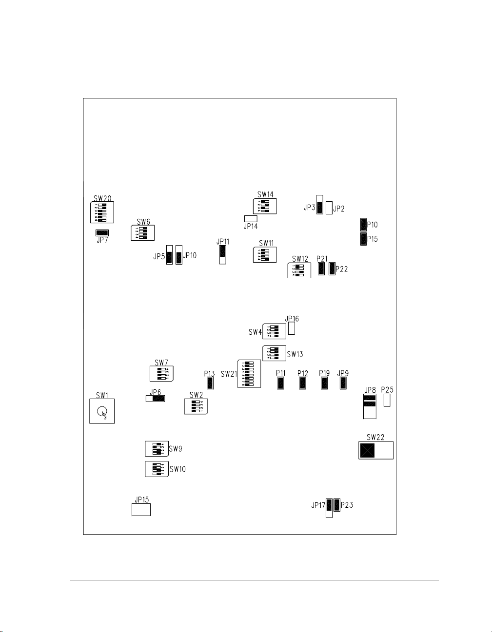
When removing the EZ-Board from the package, handle the board carefully to avoid the discharge of static electricity, which can damage some
components. Figure 1-1 shows the default jumper and switch settings,
connector locations, and LEDs used in installation. Confirm that your
board is in the default configuration before using the board.
EZ-Board Installation
For correct operation, install the software in the order presented in the
VisualDSP++ Installation Quick Reference Card. Substitute instructions in
step 3 with instructions in this section.
There are two options to connect the EZ-Board hardware to a personal
computer (PC) running VisualDSP++ 5.0: via an Analog Devices emulator or via a standalone debug agent module. The standalone debug agent
allows a debug agent to interface to the ADSP-BF526 EZ-Board. The
standalone debug agent is shipped with the kit.
1-4 ADSP-BF526 EZ-Board Evaluation System Manual
Page 27
Using ADSP-BF526 EZ-Board
Figure 1-1. Default EZ-Board Hardware Setup
ADSP-BF526 EZ-Board Evaluation System Manual 1-5
Page 28

EZ-Board Installation
To connect the EZ-Board to a PC via an emulator:
1. Set up the EZ-Board for either battery power or wall/USB power;
see “Power Setup” on page 1-29.
2. Attach the emulator header to connector
back side of the EZ-Board.
3. Depending on the power source for the EZ-Board, do one of the
following.
• Turn ON switch SW22 (battery)
• Plug the 5V wall adaptor into connector P14 (labeled 5.0V)
4. Plug the mini plug of the provided USB cable into connector P8
(labelled USB OTG). Plug the standard USB plug into a USB port of
the PC running VisualDSP++ 5.0 update 4 or newer.
To connect the EZ-Board to a PC via a standalone debug agent:
a
The debug agent can be used only when power is supplied from the
wall adaptor.
1. Attach the standalone debug agent to connectors P1 (labeled JTAG)
and ZP1 on the backside of the EZ-Board, watching for the keying
pin of P1 to connect correctly. Plug the 5V adaptor into connector
P14 (labeled 5.0V).
P1 (labeled JTAG) on the
2. Plug one side of the provided USB cable into the USB connector
ZP1) of the standalone debug agent. Plug the other side of the
(
cable into a USB port of the PC running VisualDSP++ 5.0 update
4 or newer.
1-6 ADSP-BF526 EZ-Board Evaluation System Manual
Page 29

Using ADSP-BF526 EZ-Board
The other USB connector on the ADSP-BF526 EZ-Board (labelled
USB OTG, P8) is for applications use.
3. Verify that the yellow USB monitor LED on the standalone debug
agent (LED4, located near the USB connector) is lit. This signifies
that the board is communicating properly with the host PC and
ready to run VisualDSP++.
EZ-Board Session Startup
1. If you are running VisualDSP++ for the first time, navigate to the
VisualDSP++ environment via the Start–>Programs menu. The
main window appears. Note that VisualDSP++ is not connected to
any session. Skip the rest of this step to step 2.
If you have run VisualDSP++ previously, the last opened session
appears on the screen. You can override the default behavior and
force VisualDSP++ to start a new session by pressing and holding
down the Ctrl key while starting VisualDSP++. Do not release the
Ctrl key until the Session Wizard appears on the screen. Go to
step 3.
2. To connect to a new EZ-KIT Lite session, start Session Wizard by
selecting one of the following.
• From the Session menu, New Session.
• From the Session menu, Session List. Then click New Ses-
sion from the Session List dialog box.
• From the Session menu, Connect to Target.
3. The Select Processor page of the wizard appears on the screen.
Ensure Blackfin is selected in Processor family. In Choose a target
processor, select ADSP-BF526. Click Next.
ADSP-BF526 EZ-Board Evaluation System Manual 1-7
Page 30

EZ-Board Session Startup
4. The Select Connection Type page of the wizard appears on the
screen. For standalone debug agent connections, select EZ-KIT
Lite and click Next. For emulator connections select Emulator,
and click Next
5. The Select Platform page of the wizard appears on the screen.
For standalone debug agent connections, ensure that the selected
platform is ADSP-BF526 EZ-KIT Lite via Debug Agent. For
emulator connections, choose the type of emulator that is connected. Specify your own Session name for the session or accept
the default name.
The session name can be a string of any length; although, the box
displays approximately 32 characters. The session name can
include space characters. If you do not specify a session name,
VisualDSP++ creates a session name by combining the name of the
selected platform with the selected processor. The only way to
change a session name later is to delete the session and open a new
session.
Click Next.
6. The Finish page of the wizard appears on the screen. The page dis-
plays your selections. Check the selections. If you are not satisfied,
click Back to make changes; otherwise, click Finish. VisualDSP++
creates the new session and connects to the EZ-Board. Once connected, the main window’s title is changed to include the session
name set in step 5.
L
1-8 ADSP-BF526 EZ-Board Evaluation System Manual
To disconnect from a session, click the disconnect button
or select Session–>Disconnect from Target.
To delete a session, select Session –> Session List. Select the ses-
sion name from the list and click Delete. Click OK.
Page 31

Using ADSP-BF526 EZ-Board
Evaluation License Restrictions
The ADSP-BF526 EZ-Board installation is part of the VisualDSP++
installation. The EZ-Board is a licensed product that offers an unrestricted
evaluation license for the first 90 days. Once the initial unrestricted
90-day evaluation license expires:
• VisualDSP++ restricts a connection to the ADSP-BF526 EZ-Board
via the USB port of the standalone debug agent interface only.
Connections to simulators and emulation products are no longer
allowed.
• The linker restricts a user’s program to 20 KB of memory for code
space with no restrictions for data space.
• The EZ-Board hardware must be connected and powered up to use
VisualDSP++ with a valid evaluation or permanent license.
Refer to the VisualDSP++ Installation Quick Reference Card for details.
Memory Map
The ADSP-BF526 processor has internal static random access memory
(SRAM) used for instructions and data storage. See Table 1-1. The internal memory details can be found in the ADSP-BF52x Blackfin Processor
Hardware Reference.
The ADSP-BF526 EZ-Board includes four types of external memory: synchronous dynamic random access memory (SDRAM), serial peripheral
interconnect (SPI), parallel flash, and NAND flash. See Table 1-2. For
more information about a specific memory type, go to the respective section in this chapter.
ADSP-BF526 EZ-Board Evaluation System Manual 1-9
Page 32

Memory Map
Table 1-1. EZ-Board Internal Memory Map
Start Address Content
0xEF00 0000 BOOT ROM (32K BYTE)
0xEF00 8000
0xFEB0 0000
0xFEB2 0000
0xFF40 0000
0xFF40 4000
0xFF40 8000
0xFF50 0000
0xFF50 4000
0xFF50 8000
0xFF60 0000
0xFF60 4000
0xFF60 8000
0xFF60 C000
0xFF61 0000
0xFF61 4000
0xFF70 0000
0xFF70 1000
Reserved
0xFF80 0000 L1 DATA BANKA SRAM (16K BYTE)
0xFF80 4000 L1 DATA BANKA SRAM/CACHE (16K BYTE)
0xFF80 8000 Reserved
0xFF90 0000 L1 DATA BANKB SRAM (16K BYTE)
0xFF90 4000 L1 DATA BANKB SRAM/CACHE (16K BYTE)
0xFF90 8000 Reserved
0xFFA0 0000 L1 INSTRUCTION BANKA LOWER SRAM (16K BYTE)
0xFFA0 4000 L1 INSTRUCTION BANKA UPPER SRAM (16K BYTE)
0xFFA0 8000 L1 INSTRUCTION BANKB LOWER SRAM (16K BYTE)
0xFFA0 C000 Reserved
0xFFA1 0000 L1 INSTRUCTION SRAM/CACHE (16K BYTE)
1-10 ADSP-BF526 EZ-Board Evaluation System Manual
Page 33

Using ADSP-BF526 EZ-Board
Table 1-1. EZ-Board Internal Memory Map (Cont’d)
Start Address Content
0xFFA1 4000
0xFFA1 8000
0xFFA1 C000
0xFFA2 0000
0xFFA2 4000
0xFFB0 0000 L1 SCRATCHPAD SRAM (4K BYTE)
0xFFB0 1000 Reserved
0xFFC0 0000 SYSTEM MMR REGISTERS
0xFFE0 0000 CORE MMR REGISTERS
Reserved
Table 1-2. EZ-Board External Memory Map
Start Address End Address Content
0x0000 0000 0x03FF FFFF SDRAM bank 0 (SDRAM)
0x2000 0000 0x200F FFFF ASYNC memory bank 0 (flash)
0x2010 0000 0x201F FFFF ASYNC memory bank 1 (flash)
0x2020 0000 0x202F FFFF ASYNC memory bank 2 (flash)
0x2030 0000 0x203F FFFF ASYNC memory bank 3 (flash)
0x2040 0000 0xEEFF FFFF Reserved
ADSP-BF526 EZ-Board Evaluation System Manual 1-11
Page 34

SDRAM Interface
SDRAM Interface
The ADSP-BF526 processor connects to a 64 MB Micron
MT48H32M16-75 chip through the external bus interface unit (EBIU).
The SDRAM chip can operate at a maximum clock frequency of 80 MHz,
which is the ADSP-BF526 processor limitation when operating VDDEXT
at 1.8V.
With a VisualDSP++ session running and connected to the EZ-Board via
the USB standalone debug agent, the SDRAM registers are configured
automatically each time the processor is reset. The values are used whenever SDRAM is accessed through the debugger (for example, when
viewing memory windows or loading a program).
To disable the automatic setting of the SDRAM registers, select Target
Options from the Settings menu in VisualDSP++ and uncheck Use XML
reset values. For more information on changing the reset values, refer to
the online Help.
An example program is included in the EZ-Board installation directory to
demonstrate how to setup and access the SDRAM interface. For more
information on how to initialize the registers after a reset, search the VisualDSP++ online Help for “reset values”.
Parallel Flash Memory Interface
The parallel flash memory interface of the ADSP-BF526 EZ-Board contains a 4 MB (2M x 16 bits) 1.8V Numonyx M58WR032KB chip. Flash
memory connects to the 16-bit data bus and address lines 1 through 19.
Chip enable is decoded by the AMS0—3 select lines through NAND and
AND gates. The address range for flash memory is 0x2000 0000 to
0x203F FFFF.
1-12 ADSP-BF526 EZ-Board Evaluation System Manual
Page 35

Using ADSP-BF526 EZ-Board
Flash memory is pre-loaded with boot code for the blink and
power-on-self test (POST) programs. For more information, refer to
“Power-On-Self Test” on page 1-32. Flash memory also is preloaded with
configuration flash information, which contains board revision, BOM
revision, and other data.
By default, the EZ-Board boots from the 16-bit parallel flash memory.
The processor boots from flash memory if the boot mode select switch
(
SW1) is set to a position of 1 (see “Boot Mode Select Switch (SW1)” on
page 2-10).
Flash memory code can be modified. For instructions, refer to the online
Help and example program included in the EZ-Board installation
directory.
NAND Flash Interface
The ADSP-BF526 processor is equipped with an internal NAND flash
controller, which allows the 2 Gb 1.8V ST Micro’s NAND02 device to be
attached gluelessly to the processor. NAND flash is attached via the processor’s specific NAND flash control and data lines. NAND flash shares
pins with the Ethernet PHY, host connector, and expansion interface II.
The NAND chip enable signal (NDCE#_HOSTD10) can be disconnected from
NAND flash by turning
that NAND flash is not driving data when HOSTD10 changes state. See
“Rotary/NAND Enable Switch (SW13)” on page 2-14 for more
information.
ADSP-BF526 EZ-Board Evaluation System Manual 1-13
SW13.4 (switch 13 position 4) OFF. This ensures
Page 36

SPI Interface
The Ethernet PHY (
U29) must be disabled in order for NAND flash to
function properly. This is accomplished by setting switch SW12 to OFF, OFF,
ON, OFF.
For more information about the NAND02 device, refer to the Numonyx
Web site at:
http://www.numonyx.com/en-US/MemoryProducts/NAND/Pages/
SLCLargePage.aspx
.
An example program is included in the EZ-Board installation directory to
demonstrate how to setup and access the NAND flash interface.
SPI Interface
The ADSP-BF526 processor has one serial peripheral interface (SPI) port
with multiple chip select lines. The SPI port connects directly to serial
flash memory, audio codec, and expansion interface II.
Serial flash memory is a 4 Mb SST SST25WF040 device, which is selected
using the SPISEL1 line of the processor.
SPI flash memory is factory programmed with Das U-Boot—the universal
boot loader. Das U-Boot (U-Boot for short) is open source firmware for
embedded processors, including the ADSP-BF526 Blackfin processors.
U-Boot can load files from a variety of peripherals, such as a serial connection, an Ethernet network connection, or flash memories. U-Boot is
executed at system reset, which automatically loads up another application
(such as the Linux kernel or a stand alone application). U-Boot can parse
many types of files on many types of storage devices.
U-Boot is controlled via a serial communications, the default setting is
56700 baud, 8 data bits, No parity, 1 stop bit. See “RS-232 Connector
(J2)” on page 2-32 for information on the serial connector.
1-14 ADSP-BF526 EZ-Board Evaluation System Manual
Page 37

Using ADSP-BF526 EZ-Board
For more information about U-Boot, refer to the online documentation:
http://docs.blackfin.uclinux.org/doku.php?id=bootloaders:u-boot.
For U-Boot support on the Blackfin processors, refer to the online help
forums:
http://blackfin.uclinux.org/gf/project/u-boot/forum/?action=
ForumBrowse&forum_id=51.
SPI flash can be modified. For instructions, refer to the VisualDSP++
online Help, example program included in the EZ-Board installation
directory, and U-Boot documentation. U-Boot includes an SPI flash
driver and can be used to download a new file over Ethernet or serial connection, and write that to SPI flash.
By default, the EZ-Board boots from the 16-bit flash parallel memory. SPI
flash can be selected as the boot source by setting the boot mode select
switch (SW1) to position 3 (see “Boot Mode Select Switch (SW1)” on
page 2-10).
Parallel Peripheral Interface (PPI)
The ADSP-BF526 processor provides a parallel peripheral interface (PPI),
supporting data widths up to 16 bits. The PPI interface provides three
multiplexed frame syncs, a dedicated clock input, and 16 data lines. The
full PPI port is accessible on the expansion interface II connector (
The PPI signals connect to multi-function pins; the upper eight data bit
signals are configured for the rotary, SPI,
use the upper eight PPI data lines at connector
UART1, and LED0 interfaces. To
P3, change the board as fol-
lows: disable rotary switch (SW13 positions 1–3 OFF) and disable the UART1
interface (remove a jumper from
JP3). LED0 mimics the PPID8 data pin.
The PPI has a dedicated clock, generated from the expansion interface II.
The PPI is not used on the EZ-Board, intended for use on the expansion
interface II.
ADSP-BF526 EZ-Board Evaluation System Manual 1-15
P3).
Page 38

Rotary Encoder Interface
Rotary Encoder Interface
The ADSP-BF526 processor has a built-in, up-down counter with support
for a rotary encoder. The three-wire rotary encoder interface connects to
the thumbwheel rotary switch (SW13) and expansion interface II connector
(P3). The rotary encoder can be turned clockwise for the up function,
counter clockwise for the down function, or can be pushed towards the
center of the board to clear the counter.
The rotary switch is a two-bit quadrature (gray code) counter with a
detent, meaning that both the down signal (CDG) and up signal (CUD) toggle when the count register increases on a rotation to the right. Upon
rotating to the left, CDG and CUD toggle, and the overall count decreases.
If the processor pins are needed for the expansion interface II, disconnect
the rotary encoder switch via the four-position rotary/NAND enable
switch (SW13). For more information, see “Rotary/NAND Enable Switch
(SW13)” on page 2-14.
An example program is included in the EZ-Board installation directory to
demonstrate how to set up and access the rotary encoder interface.
Ethernet Interface
The ADSP-BF526 processor has an integrated Ethernet MAC with media
independent interface (MII) and reduced media independent interface
(RMII), which connects to an external PHY. The EZ-Board provides a
SMSC LAN8700 RMII Ethernet PHY with Auto-MDIX, fully compliant
with IEEE 802.2/802.2u standards. The SMSC LAN8700 chip supports
10BASE-T and 100BASE-TX operations. The part is attached gluelessly
to the processor.
1-16 ADSP-BF526 EZ-Board Evaluation System Manual
Page 39

Using ADSP-BF526 EZ-Board
The Ethernet signals are shared with NAND flash; by default, the Ethernet mode is set
(SW12)” on page 2-14 for more information.
OFF (SW12 OFF, OFF, ON, OFF). See “ETH Enable Switch
[
The Ethernet mode is set by the SW11 switch and defaults to all capable,
auto negotiation with settings OFF, OFF, OFF, ON. See “ETH Mode/Flash
CS Switch (SW11)” on page 2-13 for more information.
The Ethernet chip is pre-loaded with a MAC address. The MAC address
for the EZ-Board is stored in the configuration flash section of the parallel
flash memory and can be found on a sticker on the bottom side of the
board.
The PHY portion of the Ethernet chip connects to a Pulse HX1188 magnetics (U28), then to a standard RJ-45 Ethernet connector (J5). For more
information, see “Ethernet Connector (J5)” on page 2-33.
Example programs are included in the EZ-Board installation directory to
demonstrate how to use the Ethernet interface.
In low-power consumption applications that do not require Ethernet, the
P21—22 jumpers can be removed to disconnect the power from the
LAN8700 PHY and Ethernet oscillator. For more information, see “ETH
PWR Jumpers (P21–22)” on page 2-27.
It is important not to run code that accesses NAND flash while
using the Ethernet interface.
Audio Interface
The audio interface of the EZ-Board consists of a low-power stereo codec,
ADI SSM2603, with an integrated headphone driver and associated passive components. There are two inputs, a stereo line in, and a mono
microphone, as well as two outputs, a headphone, and a stereo line out.
ADSP-BF526 EZ-Board Evaluation System Manual 1-17
Page 40

Audio Interface
The codec has integrated stereo analog-to-digital converters (ADCs) and
digital-to-analog converters (DACs) and requires minimal external
circuitry.
The codec connects to the ADSP-BF526 processor via the processor’s
serial port 0A (alternate). The
SPORT0A port and 2-wire interface (TWI)
are disconnected from the codec by turning switches SW2 and SW7 OFF,
which enable SPORT0A on the expansion interface II. See “SPORT0A
ENBL Switches/I2C ENBL (SW2 and SW7)” on page 2-11 for more
information.
The TWI of the ADSP-BF526 processor is used to setup and control the
codec. The default TWI address is 0011011. The TWI can be disconnected from the codec by turning positions 3 and 4 of SW2 OFF. Refer to
“SPORT0A ENBL Switches/I2C ENBL (SW2 and SW7)” on page 2-11
for more information.
Mic gain values of 14 dB, 0 dB, or –6 dB are selectable through the SW9
switch by turning ON position 1, 2, or 3 (respectively). All other positions
must be OFF to achieve the desired gain. For more information, see “MIC
Gain Switch (SW9)” on page 2-12.
Microphone bias is provided through a low-noise reference voltage. A
jumper on positions 2 and 3 of JP6 connects the MICBIAS signal to the
audio jack. Placing a jumper on positions 1 and 2 of JP6 connects the bias
directly to the mic signal. For more information, see “MIC Select Jumper
(JP6)” on page 2-22.
J3 and J4 are 3.5 mm connectors for the audio portion of the board. J4
connects the mic on the top portion and line-in on the bottom.
J3 con-
nects the headphone on the top portion and line-out on the bottom. If
there is no 3.5 mm cable plugged into the bottom of either
J3 or J4, the
signals are looped back inside the connector. For more information, see
“Dual Audio Connectors (J3–4)” on page 2-32.
1-18 ADSP-BF526 EZ-Board Evaluation System Manual
Page 41

Using ADSP-BF526 EZ-Board
For testing,
left or right headphone. Do not connect the left and right to the MICIN signal at the same time—only position 1 or 2 of SW10 should be ON at the
same time. For more information, see “Audio LPBK (Loopback) Switch
(SW10)” on page 2-13. Positions 3 and 4 of SW10 disconnect the line in
from line out loopback.
The EZ-Board is shipped with two 3.5 mm cables, which allow you to run
the example programs provided in the EZ-Board installation directory and
learn about the audio interface.
SW10 positions 1 and 2 connect the MICIN signal to either the
USB OTG Interface
The ADSP-BF526 processor has a built-in, high-speed USB OTG interface and integrated PHY. The interface connects to a 24 MHz crystal (Y2),
has a surge protector, and can be configured as a host or a device. When in
device mode, the USB 5V FET switch (U23) is turned OFF. When in host
mode, the ADSP-BF526 EZ-Board can supply 5V to a device, if desired.
L
A 5V, 500 mA current can be supplied only when the EZ-Board is
powered from the 5V wall source.
The 5V supplied to an external USB device is controlled by the PG13 flag
pin of the processor. PG13 must be connected on the board to signal
USB_VRSEL through switch SW20. The USB_VRSEL signal controls an Analog
Devices ADM869L p-channel FET, which has an active low ON pin. By
default,
connects the 5V wall supply to VBUS. To set host mode and provide 5V to
a device, set
push button 2. Note that signal HOSTADDR is shared with push button 2; do
not use the push button when controlling the
By default,
and shut off the p-channel FET (U23). For more information, see “GPIO
Enable Switch (SW20)” on page 2-17.
ADSP-BF526 EZ-Board Evaluation System Manual 1-19
USB_VRSEL is held high or a logic ‘1’ via a pull-up resistor and dis-
SW20 positions 2 and 5 OFF and position 6 ON. This disables
USB_VRSEL signal.
SW20 positions 2, 5, and 6 are ON, OFF, and OFF (respectively)
Page 42

UART Interface
The USB OTG interface has a mini-AB connector (
P8); a cable that plugs
into P8 is shipped with the EZ-Board.
Use the example programs in the EZ-Board installation directory to learn
about the ADSP-BF526 processor’s device and host modes. For more
information about the USB interface, refer to the ADSP-BF52x Blackfin
Processor Hardware Reference.
UART Interface
The ADSP-BF526 processor has two built-in universal asynchronous
receiver transmitters (UARTs). UART0—1 share the processor pins with
other peripherals on the EZ-Board.
UART1 has full RS-232 functionality via the Analog Devices 3.3V
ADM1385 line driver and receiver (U21). The ADSP-BF526 processor is
running at the VDDEXT voltage of 1.8V, requiring a voltage translator
(U32) to translate the 1.8V processor signals to the UART 3.3V line
transceiver.
The UART1 interface is disconnected from the ADM1385 transceiver by
ensuring that no jumper is installed on JP3. The ADM1385 transceiver is
shut down by placing a jumper on JP14. The UART1 interface is controlled
by the inverted WAKEUP_OUT signal, ~WAKEUP_OUT. To set up ~WAKEUP_OUT,
place a jumper on the
and 2 of JP3 disables the voltage translator, disconnecting the ADM1385
device from the
UART1 interface of the processor. This JP3 setting does not
shut down the transceiver. For more information on power saving capabilities of the EZ-Board, see “UART Enable Jumper (JP3)” on page 2-21 and
“UART SD Jumper (JP14)” on page 2-24.
JP3 positions 1 and 2. A jumper on positions 1
SW14 allows the flow control signals to be looped back. See “UART Setup
Switch (SW14)” on page 2-15 for more information.
1-20 ADSP-BF526 EZ-Board Evaluation System Manual
Page 43

Using ADSP-BF526 EZ-Board
When using
UART1, do not install jumper JP2. JP2 is a UART loopback
jumper and should be installed only when running the POST program. If
signals RTS and CTS are needed for flow control, the UART1RTS port pin
PF10 can be configured as a general-purpose I/O (GPIO) pin for RTS. The
HWAIT port pin PG0 can be used for CTS by setting up the pin accordingly;
see “UART Loopback Jumper (JP2)” on page 2-21 and “UART Enable
Jumper (JP3)” on page 2-21 for more information.
UART0 and UART1 are connected to the expansion interface II at connectors
P2 and P4. For more information, see “Expansion Interface II Connectors
(P2 and P4)” on page 2-34.
Example programs are included in the EZ-Board installation directory to
demonstrate UART and RS-232 operations.
On the processor, UART1 shares pins with the PPI interface; conse-
L
quently, do not use UART1 at the same time as the PPI interface. To
disable the UART line drive, ensure that JP3 has no jumpers on.
For more information on the UART interface, refer to the ADSP-BF52x
Blackfin Processor Hardware Reference.
RTC Interface
The ADSP-BF526 processor has a real-time clock (RTC) and a watchdog
timer. Typically, the RTC interface is used to implement a real-time
watchdog or a life counter of the time elapsed since the last system reset.
The EZ-Board is equipped with a Panasonic CR1632 lithium coin, 3V
battery supplying 125 mAh. The 3V battery and 3.3V supply of the board
connect to the
powered, the RTC circuit uses the board power to supply voltage to the
RTC pin. When the EZ-Board is not powered, the RTC circuit uses the
lithium battery to maintain the power to the
mylar, the battery lasts for about one year with the EZ-Board unpowered.
ADSP-BF526 EZ-Board Evaluation System Manual 1-21
RTC power pin of the processor. When the EZ-Board is
RTC pin. After removing the
Page 44

LEDs and Push Buttons
Example programs are included in the EZ-Board installation directory to
demonstrate the RTC features.
L
For more information on the RTC and watchdog timer, refer to the
ADSP-BF52x Blackfin Processor Hardware Reference.
The EZ-Board is shipped with a protective Mylar sheet placed
between the coin battery and positive pin of the battery holder.
Remove the Mylar sheet before using the RTC in the processor.
LEDs and Push Buttons
The EZ-Board provides two push buttons and three LEDs for general-purpose I/O and two additional push buttons intended for power
down and wake functionality, which also can be used as GPIO flag pins.
The three LEDs, labeled LED0 through LED2, are accessed via the PF8, PG11,
and PG12 pins of the processor (respectively). For information on how to
program the flag pins, refer to the ADSP-BF52x Blackfin Processor Hard-
ware Reference.
LED1 is shared with the HOSTWR# signal, while LED2 is shared with the HOSTACK
signal. The LED0 signal is shared with the PPID8 signal. When using
the PPI 16-bit data interface, LED0 mimics PPID8.
The LED1 and LED2 signals also connect to the expansion interface II (connectors
page 2-32 and “Expansion Interface II Connectors (P2 and P4)” on
page 2-34 for more information.
The two general-purpose push buttons are labeled
of each individual button can be read through programmable flag inputs
PG0 and PG13. The flag reads ‘1’ when a corresponding switch is being
pressed. When the switch is released, the flag reads ‘
between the push buttons and processor inputs is established through
positions 1 and 2 of the DIP switch, SW20.
1-22 ADSP-BF526 EZ-Board Evaluation System Manual
J1, P2, and P4). See “Expansion Interface II Connector (J1)” on
PB1 and PB2. The status
0’. A connection
Page 45

Using ADSP-BF526 EZ-Board
Push buttons 1 and 2 of
SW20 are used as GPIO signals on the expansion
interface II connectors (J1, P2, P4). To use the PG0 and PG13 port pins as
GPIO signals on the expansion interface II, turn SW20 positions 1 and 2
OFF.
Push button 1 cannot be used when PG0 is set up to control the charge rate,
when charging the battery over USB. To set this up, turn SW20.1 OFF. See
“CHG GPIO Jumper (JP15)” on page 2-24 for more information.
Push button 2 can be connected to the USB_VRSEL signal by setting
switches SW13.2 OFF, SW20.5 OFF, and SW20.6 ON. The USB_VRSEL signal
allows the USB OTG interface to power an external USB device with 5V.
Push button 2 also can be connected to the OTP_FLAG signal, which is necessary to supply 7V for writing to OTP. To set up the EZ-Board to
control the OTP_FLAG signal, set switches SW13.2 OFF, SW20.5 ON, and
SW20.6 OFF. Push button 2 is shared with signal HOSTADDR. See “USB OTG
Interface” on page 1-19 and “GPIO Enable Switch (SW20)” on page 2-17
for more information.
For a power down interrupt, signal LED2_HOSTACK is wired to SW20.3
(GPIO enable switch), which allows a push button (SW16) to drive an
interrupt to the ADSP-BF526 processor. The PG12 port pin of the processor should be set up as a GPIO pin. Turning switch SW20.3 ON connects
the push button (SW16) to the processor. By default, SW20.3 is OFF.
A wake interrupt can be set up by turning switch
processor’s flag pin
(labelled
WAKE) is pressed, PG15 receives a low-to-high transition. The PG15
PG15 as the wake interrupt. When push button SW17
SW20.4 ON and setting the
processor pin is shared with the audio codec (U31), Ethernet PHY (U29),
and HOSTCE signal. Do not use these features when using the wake interrupt push button.
An example program is included in the ADSP-BF526 installation directory to demonstrate functionality of the LEDs and push buttons.
ADSP-BF526 EZ-Board Evaluation System Manual 1-23
Page 46

JTAG Interface
JTAG Interface
The JTAG connector (P1) allows the standalone debug agent to connect a
debug session to the ADSP-BF526 processor. The debug agent operates
only when the external 5V wall adaptor is used (P14). When operating the
EZ-Board from a battery or USB bus power, the debug agent is not
powered.
The standalone debug agent can be removed, and an external emulator
can be attached to the EZ-Board. Be careful not to damage the connectors
when removing the debug agent. The emulator connects to P1 on the back
side of the board. See “EZ-Board Installation” on page 1-4 for more information. for more information.
For more information about emulators, contact Analog Devices or go to:
http://www.analog.com/processors/blackfin/evaluationDevelopment/crosscore/.
Land Grid Array
The ADSP-BF526 EZ-Board has provisions for probing every port pin
and the EBIU interface of the processor on connectors P5, P6, and P7. The
connector locations are intended for use with a Tektronix DMAX logic
analyzer connector, but can be probed with any oscilloscope or logic analyzer. Connectors
connector P7 can use either the primary or secondary retention post. For
pinout information, refer to“ADSP-BF526 EZ-Board Schematic” on
page B-1.
For more information on the Tektronix DMAX logic analyzer interface,
go to the Tektronix Web site.
1-24 ADSP-BF526 EZ-Board Evaluation System Manual
P5 and P6 require the primary retention posts, while
Page 47

Using ADSP-BF526 EZ-Board
Expansion Interface II
The expansion interface II allows an Analog Devices EZ-Extender or a
custom-design daughter board to be tested across various hardware platforms that have the same expansion interface.
The expansion interface II implemented on the ADSP-BF526 EZ-Board
consists of four connectors, three of which are 0.1 in. shrouded headers
(P2—4) and the last of which is a Samtec QMS series header (J1). The connectors contain a majority of the ADSP-BF526 processor signals. For the
pinout of the connectors, go to “ADSP-BF526 EZ-Board Schematic” on
page B-1. The mechanical dimensions of the expansion connectors can be
obtained by contacting Technical or Customer Support.
For more information about daughter boards, visit the Analog Devices
Web site at:
http://www.analog.com/processors/blackfin/evaluationDevelopment/crosscore/
.
Limits to current and interface speed must be taken into consideration
when using the expansion interface II. Current for the expansion interface
II is sourced from the EZ-Board, therefore, the current should be limited
to 1A for 5V and 500 mA for the 1.8V planes. When a battery supplies
power to the EZ-Board, the expansion interface II 5V current is reduced
to 400mA. If more current is required, then a separate power connector
and a regulator must be designed on a daughter card. Additional circuitry
can add extra loading to signals, decreasing their maximum effective
speed.
L
ADSP-BF526 EZ-Board Evaluation System Manual 1-25
Analog Devices does not support and is not responsible for the
effects of additional circuitry.
Page 48

Power Architecture
Power Architecture
The ADSP-BF526 EZ-Board has three primary voltage sources, a lithium
ion battery (740 mAh), a 5V wall adaptor, and VBUS supplied over a USB
cable. There is an OR’ing opamp circuit, which allows the board to draw
power from any supply source that has the highest voltage potential. For
example, if the battery is turned on while the board is plugged into the 5V
wall adaptor (P14), the board runs from the 5V wall adaptor.
The VDDEXT, VDDMEM, and SDRAM power are 1.8V and supplied
by an ADP2105 regulator (VR3).
The ADSP-BF526 core voltage, VDDINT, is selected via the I2C interface of the processor. The default is 1.4V. An I2C voltage translator (U39)
interfaces the 1.8V signals SDA and SCL of the processor to the AD5258
digital potentiometer (digipot, U34). The digipot sets the feedback resistors for a low drop-out (LDO) regulator ADP1715 (VR5). See the POST
example located in the ADSP-BF526 directory of VisualDSP++ to learn
how to change the VDDINT voltage. Table 1-3 shows the appropriate
step settings for the digipot and corresponding voltage values.
Table 1-3. Voltage Values
Step Value Voltage (V)
57 1.10
46 1.15
36 1.20
27 1.25
18 1.30
10 1.35
31.40
1-26 ADSP-BF526 EZ-Board Evaluation System Manual
Page 49

Using ADSP-BF526 EZ-Board
The 3.3V power for the board is regulated by an ADP2105 converter
(
VR2).
The 1.8V power for the audio ADI SSM2603 audio codec (U31) is regulated by an ADP1205 device (VR1).
The expansion interface II is equipped with three voltage domains: 5V,
3.3V, and 1.8V. The 1.8V and 3.3V are provided directly through the VR2
and VR3 regulators. The 5V is sourced from the wall adaptor when jumper
JP8 is set to positions 1, 2 and 3, 4, and JP9 is ON. The 5V also can be pro-
vided by the on-board ADP1611 converter when using the lithium ion
battery. To set up the ADP1611 converter (VR7), install jumpers on positions 5, 6 and 7, 8 of JP8 and ensure JP9 is OFF.
To write to the OTP memory inside the processor, turn SW20.2 OFF,
SW20.5 ON, and SW20.6 OFF. Also install a jumper on JP16. Now the PG13
flag pin of the processor, when driven high, provides a precise 7.0V for
OTP writes. Ensure that the PG13 flag pin is driven low when not writing
to the OTP memory: there is a limited amount of time that the OTP circuit can be supplied 7V. Refer to the ADSP-BF526 data sheet for more
information.
a
In USB host mode, if the host must provide 5V to a device, the
pin must be set low to turn on the p-channel mosfet (
PG13 of the processor to the mosfet, set SW20.2 OFF, SW20.5 OFF, and
SW20.6 ON.
The lithium ion battery leads are inserted into the P24 connector. The
SW22 switch connects the battery to the EZ-Board when SW22 is ON. To
change the battery, press in the white tabs and slide out the battery lead.
L
ADSP-BF526 EZ-Board Evaluation System Manual 1-27
Leaving JP16 ON when not writing to the OTP memory can damage
the processor. See the ADSP-BF522/523/524/525/526/527 Blackfin
Embedded Processor Data Sheet.
PG13 flag
U23). To connect
The EZ-Board is intended to be used at room temperature
(approximately 21
o
C)
Page 50

Power Architecture
An ADP2291 lithium ion battery charger IC charges the 740 mAh battery. The charge rate is selected based on a jumper placement and whether
the battery is charging from a wall adaptor or from a USB port. See
Table 1-4 for details.
Table 1-4. Charge Rate Selection
Mode WALL USB JP17 P23 Resistance Charge Rate
Full Charge YES NO X
Low NO YES OFF OFF 32K 100 mA
Medium NO YES 2 and 3 X 169K 375 mA
Selectable
Shutdown NO YES OFF ON 0 NONE
2
NO YES 1 and 2 OFF 32/169K 100/375 mA
1
XOPEN 750mA
Control Shut-
3
down
1 Any jumper setting has no affect.
2 Rate is selectable by the processor’s flag: use JP15 to chose the flag pin. Setting the flag high se-
lects 83 mA and setting the flag low selects 375 mA charge rates.
3 JP15 needs to be set to positions 1and 2 (PG0), 3 and 4 (PG11), or 5 and 6 (PG12), selecting
the processor port pin to control the selection. See “CHG GPIO Jumper (JP15)” on page 2-24
for more information.
The lithium battery is monitored by the BQ27500 fuel gauge (
NO YES 1 and 2 ON 0/169K 0/375mA
U38). All
battery statistics can be read from the fuel gauge, including time to empty,
current voltage, and current consumption rate.
SW4 positions 1 and 2 dis-
connect the fuel gauge LED signals. SW4 positions 3 and 4 disconnect the
TWI signals from the processor and fuel gauge. For more information
about
SW4, refer to “Gauge Signals Switch (SW4)” on page 2-11. An exam-
ple program in the POST directory of the ADSP-BF526 EZ-Board
installation demonstrates how to use the fuel gauge.
Change jumper and switch settings only when power is OFF.
a
1-28 ADSP-BF526 EZ-Board Evaluation System Manual
Page 51

Using ADSP-BF526 EZ-Board
Power Setup
The EZ-Board is shipped with the default configuration for 5V power
from a wall adaptor or a USB port (see Table 1-5).
a
Change jumper and switch settings only when power is OFF.
Table 1-5. 5V Power Settings
Switch/Jumper 5V Setting
JP8 Positions 1 and 2, 3 and 4
JP9 Installed
JP10 Positions 2 and 3
JP15 Uninstalled
P17 Positions 1 and 2
P23 OFF
P25 OFF
SW22 OFF
To set up the board for battery operation, the settings in Table 1-6 are a
good starting point.
Table 1-6. Battery Power Settings
Switch/Jumper Battery Setting
JP8
(if 5V needed on the expansion interface II)
JP9
(if 5V needed on expansion interface II)
JP10 Positions 1 and 2
JP15 See Table 1-4
P17 See Table 1-4
Positions 5 and 6, 7 and 8
Uninstalled
ADSP-BF526 EZ-Board Evaluation System Manual 1-29
Page 52

Power Saving Features
Table 1-6. Battery Power Settings (Cont’d)
Switch/Jumper Battery Setting
P23 OFF; see Table 1-4
P25 ON
SW22 ON
Refer to the individual switch and jumper descriptions for alternate
settings.
L
ing the charging rate and implementation of power saving features.
Power Saving Features
The ADSP-BF526 EZ-Board is designed for low-power application evaluations; use the following settings to enable the board’s power saving
features.
• Jumper-controlled power savings:
D The Ethernet PHY (SMSC LAN8700) can be totally pow-
ered down by removing jumpers P21 and P22.
D The UART line drivers can be powered down by placing a
Note that complying with USB current limitations requires limit-
jumper on
D The reset and Ethernet LED voltage translator can be dis-
abled by removing any jumper from JP11.
D The GPIO LED’s and OTP flag voltage translator can be
disabled by removing any jumper from
JP14 and then removing any jumper from JP3.
JP5.
1-30 ADSP-BF526 EZ-Board Evaluation System Manual
Page 53

Using ADSP-BF526 EZ-Board
• Processor-controlled power savings:
The VDDINT regulator (
VR5) can be shut down with the EXT_WAKE
signal of the processor. EXT_WAKE also controls:
D The OTP flag and LED voltage translator (U3) via JP5
D
The Ethernet LED and reset voltage translator (U4) via JP11
D
The UART1 voltage translator (U32) via JP3
Refer to the ADSP-BF52x Blackfin Processor Hardware Reference for
more information about EXT_WAKE; refer to “Jumpers” on page 2-20
for more information about the jumpers.
• Low-power mode capable ICs of the EZ-Board:
D ADI SSM2603 audio codec (U31)
D Micron MT48H32M16-75 SDRAM memory (U14)
D Numonyx M58WR032KB parallel flash (U16)
D SST 25WF040 SPI flash memory (U6)
D Numonyx NAND02 flash memory (U15)
Some of the low-power modes are entered by inactivity on-chip select
lines. Consult the product data sheets for details.
Power Measurements
Several locations are provided for measuring the current draw from various power planes. Precision 0.1 ohm shunt resistors are available on the
VDDINT, VDDEXT, VDDMEM, and SDRAM voltage domains. For
current draw measuments, the associated jumper (P13, P11, P12, or P19)
should be removed. Once the jumper is removed, the voltage across the
ADSP-BF526 EZ-Board Evaluation System Manual 1-31
Page 54

Power-On-Self Test
resistor can be measured using an oscilloscope. Once voltage is measured,
current can be calculated by dividing the voltage by 0.1. For the highest
accuracy, a differential probe should be used for measuring voltage across
the resistor.
For more information, see “VDDINT Power Jumper (P13)” on
page 2-26, “VDDEXT Power Jumper (P11)” on page 2-26, and
“VDDMEM Power Jumper (P12)” on page 2-26.
Power-On-Self Test
The power-on-self-test program (POST) tests all EZ-Board peripherals
and validates functionality as well as connectivity to the processor. Once
assembled, each EZ-Board is fully tested for an extended period of time
with a POST; all EZ-Boards are shipped with the POST preloaded into
one of its on-board flash memories. The POST is executed by resetting the
board and pressing the proper push button(s). The POST also can be used
for reference for a custom software design or hardware troubleshooting.
Note that the source code for the POST program is included in the VisualDSP++ installation directory, along with the readme text file, which
describes how the EZ-Board is configured to run POST.
Example Programs
Example programs are provided with the ADSP-BF526 EZ-Board to demonstrate various capabilities of the product. The programs are installed
with the VisualDSP++ software and can be found in the
<install_path>\Blackfin\Examples\ADSP-BF526 EZ-Board directory.
Refer to the readme file provided with each example for more
information.
1-32 ADSP-BF526 EZ-Board Evaluation System Manual
Page 55

Using ADSP-BF526 EZ-Board
Background Telemetry Channel
The USB debug agent supports the background telemetry channel (BTC),
which facilitates data exchange between VisualDSP++ and the processor
without interrupting processor execution.
The BTC allows you to read and write data in real time while the processor continues to execute. For increased performance of the BTC,
including faster reading and writing, please check our latest line of processor emulators at:
http://www.analog.com/en/embedded-processing-dsp/sharc/USB-EMULATOR/products/product.html
online help.
. For more information about BTC, see the
Reference Design Information
A reference design info package is available for download on the Analog
Devices Web site. The package provides information on the design, layout, fabrication, and assembly of the EZ-KIT Lite and EZ-Board
products.
The information can be found at:
http://www.analog.com/en/evaluation-boards-kits/resources/embedded-processing-dsp/blackfin/index.html.
ADSP-BF526 EZ-Board Evaluation System Manual 1-33
Page 56

Reference Design Information
1-34 ADSP-BF526 EZ-Board Evaluation System Manual
Page 57

2 ADSP-BF526 EZ-BOARD
HARDWARE REFERENCE
This chapter describes the hardware design of the ADSP-BF526 EZ-Board
board.
The following topics are covered.
• “System Architecture” on page 2-2
Describes the ADSP-BF526 EZ-Board configuration and explains
how the board components interface with the processor.
• “Programmable Flags” on page 2-3
Shows the locations and describes the programming flags (PFs).
• “Push Button and Switch Settings” on page 2-9
Shows the locations and describes the push buttons and switches.
• “Jumpers” on page 2-20
Shows the locations and describes the configuration jumpers.
• “LEDs” on page 2-28
Shows the locations and describes the LEDs.
• “Connectors” on page 2-31
Shows the locations and provides part numbers for the on-board
connectors. In addition, the manufacturer and part number information is provided for the mating parts.
ADSP-BF526 EZ-Board Evaluation System Manual 2-1
Page 58

System Architecture
ADSP-BF525
DSP
400 MHz
12mmX12mm/0.5 pitch
LEDs (3)
1.8 Volts
EBIU
JTAG
Port
32.768 KHz
Crystal
3.3 volt
RTC
SPI
64 MB
SDRAM
(32M x 16)
1.8 Volts
High
Density
EBIU
Expansion
Interface
4 MB
Flash
(2M x 16 )
1.8 Volts
25 MHz
Crystal
1.8 Volts
UARTs
PBs (2)
1.8 Volts
RS-232
Female
RS-232
TX/RX
3.3 Volts
SPORT PPI
MAC USB
Ethernet Phy RMII
1.8 Volts (MAC to Phy)
3.3 Volts (Phy to Mag)
RJ11
TWI
IDC
Conn
IDC
Conn
IDC
Conn
IDC
Conn
USB OTG Conn
3.3 Volts
5 Volts source when
in Host Mode
IDC
Conn
Rotary
1.8 Volts
2 Gb
NAND Flash
(512M x 8 )
1.8 Volts
4 Mb
SPI Boot
Flash
1.8 Volts
HOST
PORT
IDC
Conn
NAND
24 MHz
Crystal
3.3 Volts
+3.0
LI-ION
Battery
CLKIN
UP/DN
CNTR
12 MHz
Crystal
1.8 Volts
Power Regulation
1.8 Volt, 3.3 Volt,
2.5 Volt, 5.0 Volt
Li Battery
Charge Circuit
GPIO
Audio
Codec
1.8 Volts
Mic/
Line
In
Head/
Line
Out
IDC
Conn
Fuel
Gauge
System Architecture
This section describes the processor’s configuration on the EZ-Board
(Figure 2-1).
2-2 ADSP-BF526 EZ-Board Evaluation System Manual
Figure 2-1. System Architecture
This EZ-Board is designed to demonstrate the capabilities of the
ADSP-BF526 Blackfin processors. The processor has an I/O voltage of
1.8V. The core voltage of the processor is controlled by an Analog Devices
ADP1715 low dropout regulator (LDO) and an Analog Devices AD5258
Page 59

ADSP-BF526 EZ-Board Hardware Reference
digipot, which is configurable over the 2-wire interface (TWI) signals.
Refer to the power-on-self test (POST) example in the ADSP-BF526
installation directory of VisualDSP++ for information on how to set up
the TWI interface.
The core voltage and clock rate can be set on the fly by the processor. The
input clock is 25 MHz. A 32.768 kHz crystal supplies the real-time clock
(RTC) inputs of the processor. The default boot mode for the processor is
external parallel flash boot. See “Boot Mode Select Switch (SW1)” on
page 2-10 for information on how to change the default boot mode.
Programmable Flags
The processor has 50 general-purpose input/output (GPIO) signals spread
across four ports (PF, PG, PH, and PJ). The pins are multi-functional and
depend on the ADSP-BF526 processor setup. The following tables show
how the programmable flag pins are used on the EZ-Board.
• PF programmable flag pins – Table 2-1
• PG programmable flag pins – Table 2-2
• PH programmable flag pins – Table 2-3
PJ programmable flag pins – Table 2-4
•
Table 2-1. PF Port Programmable Flag Connections
Processor Pin Other Processor Function EZ-Board Function
PF0 PPID0/DR0PRI/ND_D0A Default: PPID0 on P3.18 via RN1
Land grid array P7.A
PF1 PPID1/RFS0/ND_D1A Default: PPID1 on P3.17 via RN1
Land grid array P7.A2
PF2 PPID2/RSCLK0/ND_D2 Default: PPID2 on P3.20 via RN1
Land grid array P7.A4
ADSP-BF526 EZ-Board Evaluation System Manual 2-3
Page 60

Programmable Flags
Table 2-1. PF Port Programmable Flag Connections (Cont’d)
Processor Pin Other Processor Function EZ-Board Function
PF3 PPID3/DT0PRI/ND_D3A Default: PPID3 on P3.19 via RN1
Land grid array P7.A5
PF4 PPID4/TFS0/ND_D4A/
TACLK0
PF5 PPID5/TSCLK0/ND_D5A/
TACLK1
PF6 PPID6/DT0SEC/ND_D6A/
TACI0
PF7 PPID7/DR0SEC/ND_D7A/
TACI1
PF8 PPID8/DR1PRI Default: LED0 via RN2
Default: PPID4 on P3.22 via RN1
Land grid array P7.A10
Default: PPID5 on P3.21 via RN1
Land grid array P7.A11
Default: PPID6 on P3.24 via RN1
Land grid array P7.A13
Default: PPID7 on P3.23 via RN1
Land grid array P7.A14
Expansion interface II P3.26 (PPID8), P4.14 via
SW21.8, land grid array P7.A16
PF9 PPID9/RSCLK1/SPISEL6# Default: PPID9 via RN2
Expansion interface II (P3.25, P4.18) via SW21.7, land
grid array
PF10 PPID10/PRFS1/SPISEL7# Default: UART1RTS (U21) via U32, SW14.3 and RN2
P7.A17
Expansion interface II (P3.28, P4.20) via SW21.6, land
grid array P7.A17
PF11 PPID11/TFS1/CZM Default: CZM rotary (SW5) via SW13.3 and RN2
Expansion interface II (P3.27, P4.19) via SW21.5, land
P7.A20
P7.A22
PF12 PPID12/DT1PRI/
SPISEL2#/CDG
grid array
Default: CDG rotary (SW5) via SW13.2 and RN2
Expansion interface II (P3.30, P4.13) via SW21.4, land
grid array
PF13 PPID13/TSCLK1/
SPISEL3#/CUD
Default: CUD rotary (SW5) via SW13.1 and RN2
Expansion interface II (P3.29, P4.17) via SW21.3, land
grid array
P7.A23
2-4 ADSP-BF526 EZ-Board Evaluation System Manual
Page 61

ADSP-BF526 EZ-Board Hardware Reference
Table 2-1. PF Port Programmable Flag Connections (Cont’d)
Processor Pin Other Processor Function EZ-Board Function
PF14 PPID14/DT1SEC/UART1TX Default: UAR1TX (U21) via U32 and RN2
Expansion interface II (P3.32, P4.15) via SW21.2, land
grid array P7.A25
PF15 PPID15/DR1SEC/
UART1RX/TACI3
Default: UAR1RX (U21) via U32, SW14.2 and RN2
Expansion interface II (P3.31, P4.16 via SW21.1,
P4.32) via SW21.1, land grid array P7.A26
Table 2-2. PG Port Programmable Flag Connections
Processor Pin Other Processor Function EZ-Board Function
PG0 HWAIT Default: PB1 via SW21.1 and RN5
UART1 CTS (HWAIT) via U32, SW14.1, host connector
P9.12, CHG GPIO JP15.1, expansion interface II
(P2.37, P4.37, J1.52), land grid array P7.B27
PG1 SPISS#/SPISEL1# Default: SPI flash (U6) CS via SW11.4 and RN3
Expansion interface II (P2.21, P4.21, P4.26, P2.26),
land grid array P7.B26
PG2 SPISCK Default: SPI flash (U6)
Expansion interface II (P2.24, P4.24), land grid array
P7.B9
PG3 SPIMISO/DR0SECA Default: SPI flash (U6) via RN3
Expansion interface II (P2.16, P2.27, P4.27), land
grid array
PG4 SPIMOSI/DT0SECA Default: SPI flash (U6)
Expansion interface II (
grid array P7.B24
P7.B23
P2.15, P2.25, P4.25), land
PG5 TMR1/PPIFS2/TFS0A Default: PPIFS2 P3.14
Land grid array P7.B17
PG6 DT0PRIA/TMR2/PPIFS3 Default: DT0PRIA codec (U31) via SW7.2
Expansion interface II (
P7.B18
P2.13, P3.15), land grid array
ADSP-BF526 EZ-Board Evaluation System Manual 2-5
Page 62

Programmable Flags
Table 2-2. PG Port Programmable Flag Connections (Cont’d)
Processor Pin Other Processor Function EZ-Board Function
PG7 TMR3/DR0PRIA/UART0TX Default: DR0PRIA codec (U31) via SW7.3
Expansion interface II (P2.14, P2.31, P3.36), land
grid array P7.B14
PG8 TMR4/RFS0A/UART0RX/
TACI4
Default: RFS0A codec (U31) via SW7.4
Expansion interface II (
P3.35, P2.20, P2.32), land
grid array P7.B15
PG9 TMR5/RSCLK0A/TACI5 Default: RSCLK0A codec (U31) via SW2.2
Expansion interface II (P2.18, P3.38), land grid array
P7.B11
PG10 TMR6/TSCLK0A/TACI6 Default: TSCLK0A codec (U31) via SW2.1
Expansion interface II P2.17, land grid array P7.B12
PG11 TMR7/HOST_WR# Default: LED1 via U3 and RN5
CHG GPIO JP15.3, host connector P9.4, expansion
interface II (
J1.51, P2.28, P2.38, P4.28, P4.38),
land grid array P7.B6
PG12 DMAR1/UART1TXA/
HOST_ACK
PG13 DMAR0/UART1RXA/
HOST_ADDR/TACI2
PG14 TSCLK0A/MDC/HOST_RD# Default: host connector P9.2
Default: LED2 via U3 and RN5
Power down PB via SW20.3, CHG GPIO JP15.5, host
connector
P2.39, P4.39), land grid array P7.B8
P9.10, expansion interface II (J1.54,
Default: PB2 via SW21.2 and RN5
OTP_FLAG_1P8V via SW20.5, USB_VRSEL via SW20.6,
host connector
P2.40, P4.40), land grid array P7.B5
MDC PHY (U29) via SW12.2, land grid array P7.B2
P9.8, expansion interface II (J1.53,
PG15 TFS0A/MIIPHYINT#/
RMIIMDINT#/HOST_CE#
Default: TFS0A codec (U31) via SW7.1 and RN5
RMIIMDINT# PHY (U29), wake via SW20.4, host con-
nector
P9.6, expansion interface II P2.19, land grid
P7.B3
array
2-6 ADSP-BF526 EZ-Board Evaluation System Manual
Page 63

ADSP-BF526 EZ-Board Hardware Reference
Table 2-3. PH Port Programmable Flag Connections
Processor Pin Other Processor Function EZ-Board Function
PH0 ND_D0/MIICRS/
RMIICRSDV/HOST_D0
Default: NAND data 0 (U15) via RN4
RMII carrier sense/receive data valid (U29.36), host
connector data 0 (P9.31), land grid array P6.B3
PH1 ND_D1/ERXER/HOST_D1 Default: NAND data 1 (U15) via RN4
PHY receive error (U29.21), host connector data 1
(P9.29), land grid array P6.B2
PH2 ND_D2/MDIO/HOST_D2 Default: NAND data 2 (U15) via RN4
PHY management bus MDIO U29 via SW12.1, host connector data 2 (
PH3 ND_D3/ETXEN/HOST_D3 Default: NAND data 3 (U15) via RN4
P9.27), land grid array P6.B6
PHY transmit enable (U29.6), host connector data 3
(P9.25), land grid array P6.B5
PH4 ND_D4/MIITXCLK/
RMIIREF_CLK/HOST_D4
Default: NAND data 4 (U15) via RN4
PHY RMII ref clock U29 via SW12.3 and U20, host
connector data 4 (P9.23), land grid array P6.B9
PH5 ND_D5/ETXD0/HOST_D5 Default: NAND data 5 (U15) via RN4
PHY RMII transmit data 0 (U29.23), host connector
P9.21), land grid array P6.B8
data 5 (
PH6 ND_D6/ERXD0/HOST_D6 Default: NAND data 6 (U15) via RN4
PHY RMII receive data 0 (U29.18), PHY mode via
SW11.3, host connector data 6 (P9.19), land grid array
P6.B11
PH7 ND_D7/ETXD1/HOST_D7 Default: NAND data 7 (U15) via RN4
PHY RMII transmit data 1 (U29.24), host connector
data 7 (P9.17), land grid array P6.B12
PH8 SPISEL4#/ERXD1/
HOST_D8/TACLK2
PH9 SPISEL5#/ETXD2/
HOST_D9/TACLK3
Default: PHY RMII receive data 1 (U29.17) via RN5
PHY mode via SW11.2, host connector data 8 (P9.15),
expansion interface II (
P6.B15
P2.22, P4.22), land grid array
Default: host connector P9.13, expansion interface II
P2.23, P4.23, land grid array P6.B27
ADSP-BF526 EZ-Board Evaluation System Manual 2-7
Page 64

Programmable Flags
Table 2-3. PH Port Programmable Flag Connections (Cont’d)
Processor Pin Other Processor Function EZ-Board Function
PH10 ND_CE#_ERXD2/HOST_D10 Default: NAND chip (U15) enable via SW13.4
Host connector data 10 (P9.11), land grid array
P6.B26
PH11 ND_WE/ETXD3/HOST_D11 Default: NAND write enable (U15)
Host connector data 11 (
PH12 ND_RE/ERXD3/HOST_D12 Default: NAND output enable (U15)
Host connector data 12 (P9.7), land grid array P6.B21
P9.9), land grid array P6.B24
PH13 ND_BUSY/ERXCLK/
HOST_D13
PH14 ND_CLE/ERXDV/HOST_D14 Default: NAND command latch enable (U15)
PH15 ND_ALE/COL/HOST_D15 Default: NAND address latch enable (U15)
Default: NAND busy (U15)
Host connector data 13 (P9.5), land grid array P6.B23
Host connector data 14 (
P9.3), land grid array P6.B18
Host connector data 15 (P9.1), land grid array P6.B17
Table 2-4. PJ Port Programmable Flag Connections
Processor Pin Other Processor
Function
PJ0 PPIFS1/TMR0 Default: PPIFS1 P3.13
PJ1 PPICLK/TMRCLK Default: PPICLK P3.16
PJ2 SCL Default: fuel gauge U38 via switch SW4.3, digipot U34
PJ3 SDA Default: fuel gauge U38 via switch SW4.4, digipot U34
EZ-Board Function
Land grid array P7.B21
Land grid array P7.A7
U39 via RN5
via
Codec via SW2.4, expansion interface II (P2.29, P3.63,
P4.29)
U39 via RN5
via
Codec via SW2.2, expansion interface II (P2.30, P3.61,
P4.30)
2-8 ADSP-BF526 EZ-Board Evaluation System Manual
Page 65

ADSP-BF526 EZ-Board Hardware Reference
Push Button and Switch Settings
This section describes operation of the push buttons and switches. The
push button and switch locations are shown in Figure 2-2.
Figure 2-2. Push Button and Switch Locations
ADSP-BF526 EZ-Board Evaluation System Manual 2-9
Page 66

Push Button and Switch Settings
Boot Mode Select Switch (SW1)
The rotary switch (SW1) determines the boot mode of the processor.
Table 2-5 shows the available boot mode settings. By default, the
ADSP-BF526 processor boots from the on-board parallel flash memory.
L
entire rotating portion of the switch, not the small arrow.
Table 2-5. Boot Mode Select Switch (SW1)
SW1 Position Processor Boot Mode
0 Reserved
1 Boot from 8-bit external flash memory (default)
2 Boot from 16-bit asynchronous FIFO
3 Boot from serial SPI memory
4 Boot from SPI host device
5 Boot from serial TWI memory
6 Boot from TWI host
7Boot from UART0 host
8Boot from UART1 host
9 Reserved
A Boot from SDRAM
B Boot from 8-bit NAND flash PORTF
The selected position of SW1 is marked by the notch down the
C Boot from 8-bit NAND flash PORTH
D Reserved
E Boot from 16-bit host DMA
F Boot from 8-bit host DMA
2-10 ADSP-BF526 EZ-Board Evaluation System Manual
Page 67

ADSP-BF526 EZ-Board Hardware Reference
SPORT0A ENBL Switches/I2C ENBL (SW2 and SW7)
The SPORT0A enable switches (SW2 and SW7) connect the SPORT0A and TWI
interfaces of the processor to the audio codec, SSM2603 (U31). When the
SPORT0A interface is used on the expansion interface II, turn SW2 and SW7
positions 1 and 2 all OFF. To disconnect TWI to the audio codec turn SW2
positions 3 and 4 OFF. By default, SW2 and SW7 are set to all ON.
Gauge Signals Switch (SW4)
The gauge signals switch (SW4) positions 1 and 2 disconnect the fuel gauge
status LEDs from the BQ27500 fuel gauge device. Positions 3 and 4 disconnect the I2C signals from the fuel gauge. If the I2C bus hangs when
performing fast bus operations, it may be necessary to turn positions 3 and
4 OFF. By default, SW4 is set to all ON.
Rotary Encoder with Momentary Switch (SW5)
The rotary encoder (SW5) can be turned clockwise for an up count or
counter-clockwise for a down count. The encoder also features a momentary switch, activated by pushing the switch towards the processor, which
resets the counter to zero. The rotary encoder is a two-bit quadrature (gray
code) encoder. Refer to the Rotary Counter section of the ADSP-BF52x
Blackfin Processor Hardware Reference for more information.
The rotary encoder is disconnected from the processor by setting SW13
positions 1, 2 and 3 to
on page 2-14 for more information.
ADSP-BF526 EZ-Board Evaluation System Manual 2-11
OFF. See “Rotary/NAND Enable Switch (SW13)”
Page 68

Push Button and Switch Settings
Flash Enable Switch (SW6)
The flash enable switch (SW6) disconnects the ~AMSx signals from parallel
flash memory (U16), allowing other devices to utilize the signals via the
expansion interface II. For each switch listed in Table 2-6 that is turned
OFF, the size of available flash memory is reduced by 1 MB.
Table 2-6. Flash Enable Switch (SW6)
SW6 Switch Position (Default) Processor Signal
1 (ON) ~AMS0
2 (ON) ~AMS1
3 (ON) ~AMS2
4 (ON) ~AMS3
MIC Gain Switch (SW9)
The microphone gain switch (SW9) sets the gain of the MIC signal, which is
connected to the top 3.5 mm jack (J4). The gain can be set to 14 dB,
0 dB, or –6 dB by turning ON position 1, 2, or 3 of SW9 (see Table 2-7).
When the corresponding position for the desired gain is ON, the remaining
positions must be OFF. Refer to “Audio Interface” on page 1-17 for more
information about the audio codec.
Table 2-7. MIC Gain Switch (SW9)
Gain SW9 Switch Settings
5 (14 dB) ON, OFF, OFF, OFF
1 (0 dB) OFF, ON, OFF, OFF
0.5 (–6 dB) OFF, OFF, ON, OFF (default)
Unused OFF, OFF, OFF, OFF
2-12 ADSP-BF526 EZ-Board Evaluation System Manual
Page 69

ADSP-BF526 EZ-Board Hardware Reference
Audio LPBK (Loopback) Switch (SW10)
The SW10 switch places the EZ-Board in a loopback to test the board for
signal/circuit continuity and functionality. SW10 positions 1 and 2 connect
the MICIN signal to the headphone’s left and right outputs for audio loopback. Do not turn SW10 positions 1 and 2 ON at the same time. See
“Power-On-Self Test” on page 1-32 for more information.
SW10 positions 3 and 4 connects the line in to line out loopback. By
default, SW10 is set to OFF, OFF, ON, ON.
ETH Mode/Flash CS Switch (SW11)
The Ethernet mode flash CS switch (SW11) sets the bootstrapping option
for the LAN8700 RMII PHY chip (U29). The mode settings for the PHY
utilize internal chip pull-ups. Setting a position 1–3 of SW11 ON connects a
pull-down resistor. Table 2-8 shows the default as well as the alternate
switch settings.
SW11 position 4 disconnects the SPISEL1 pin from the SPI flash chip (U6).
Setting SW11 position 4 OFF is useful when using SPISEL1 on the expansion
interface II. By default, SW11 is set to OFF, OFF, OFF, ON,
Table 2-8. ETH Mode Flash CS Switch (SW11 Positions 1–3)
MODE[2:0] Setting Mode Definitions
OFF, OFF, OFF All capable, auto negotiation (default)
OFF, OFF, ON Power down mode
OFF, ON, OFF Repeater mode, auto negotiation
OFF, ON, ON 100Base-TX half duplex advertised, auto negotiation
ON, OFF, OFF 100Base-TX full duplex
ON, OFF, ON 100Base-TX half duplex
ADSP-BF526 EZ-Board Evaluation System Manual 2-13
Page 70

Push Button and Switch Settings
Table 2-8. ETH Mode Flash CS Switch (SW11 Positions 1–3) (Cont’d)
MODE[2:0] Setting Mode Definitions
ON, ON, OFF 10Base-T full duplex
ON, ON, ON 10Base-T half duplex
ETH Enable Switch (SW12)
The Ethernet enable switch (SW12) enables the Ethernet interface. The
Ethernet and NAND flash share the same lines and cannot operate at the
same time. By default, the SW12 settings are OFF, OFF, ON, OFF (see
Table 2-9). Ethernet is enabled by setting the switch to ON, ON, OFF, ON.
SW12 positions 1and 2 connect the PHY management bus (MDIO and MDC).
SW12 position 3 ON enables the 50 MHz RMII clock. SW12 position 4 holds
the PHY in reset (set to OFF) or connects the PHY reset to the EZ-Board
reset (set to ON).
Table 2-9. ETH Enable Switch (SW12)
SW12 Switch Setting Ethernet Mode
OFF, OFF, ON, OFF OFF (default)
ON, ON, OFF, ON ON
Rotary/NAND Enable Switch (SW13)
The rotary/NAND enable switch (SW13) disconnects the rotary encoder
signals from the GPIO pins of the processor. When SW13 is OFF, its associated GPIO signals can be used on the expansion interface II (see
Table 2-10). Position 4 of SW13 disconnects the chip enable for the
NAND flash memory (U4).
2-14 ADSP-BF526 EZ-Board Evaluation System Manual
Page 71

ADSP-BF526 EZ-Board Hardware Reference
Table 2-10. Rotary NAND Enable Switch (SW13)
SW13 Position (Default) From To
1 (ON)Encoder (SW5)Processor (U1, PF13)
2 (ON)Encoder (SW5)Processor (U1, PF12)
3 (ON)Encoder (SW5)Processor (U1, PF11)
4 (ON)Processor (U1, PH10) NAND (U15)
UART Setup Switch (SW14)
The UART setup switch (SW14) configures the UART1 signals from the
GPIO pins of the processor. By default, SW14 is OFF, ON, OFF, ON. Flow con-
trol is not implemented in the POST program, so SW14 positions 1 and 3
should be OFF and position 4 should be ON for loopback flow control.
Refer to the ADM1385 data sheet on the Analog Devices Web Site for
more information about the UART interface.
Programmable Flag Push Buttons (SW15 and SW19)
Two momentary push buttons (SW15 and SW19) are provided for general-purpose user input. The buttons connect to the PG0 and PG13 GPIO
pins of the processor. The push buttons are active high and, when pressed,
send a high (
1) to the processor. The GPIO enable switch (SW20) discon-
nects the push buttons from the corresponding push button signals. Refer
to “GPIO Enable Switch (SW20)” on page 2-17 for more information.
Power-Down and Wake Push Buttons (SW16–17)
Two momentary push buttons (SW16—17) are provided for optional power
feature inputs. The buttons connect to the
the processor. The push buttons are active high and, when pressed, send a
ADSP-BF526 EZ-Board Evaluation System Manual 2-15
PG12 and PG15 GPIO pins of
Page 72

Push Button and Switch Settings
high (
1) to the processor. The GPIO enable switch (SW20) disconnects the
push buttons from the corresponding push buttons signals. Refer to
“GPIO Enable Switch (SW20)” on page 2-17 for more information.
The power-down push button (SW16) is intended as an GPIO input to the
processor and can be configured to put the processor in any one of the
sleep modes.
The wake push button (SW17) is connected to the flag pin (PG15), which
can be configured as the dedicated WAKE input signal from hibernation.
Refer to the ADSP-BF52x Blackfin Processor Hardware Reference Manual
for more information.
Reset Push Button (SW18)
The reset push button (SW18) resets the following ICs.
• Processor (U1), parallel flash (U16), PHY (U29) if SW12 position 4 is
ON, SPI flash (U6)
The reset push button does not reset the following ICs.
•SDRAM (U14), NAND flash (U15)
• Audio codec (U31), UART1 (U21), voltage translators (U3, U4, U32,
U39) schmitt trigger hex inverter (U5)
• Fuel gauge (
3
, VR5, VR9, VR10, U23)
U38), digipot (U34), battery charger (U37), power (VR2—
The reset push button does not reset the standalone debug agent once the
debug agent is connected to a personal computer (PC). After communication between the debug agent and PC is initialized, pushing a reset button
does not reset the USB chip on the debug agent. The only way to reset the
USB chip on the debug agent is to power down the EZ-Board.
2-16 ADSP-BF526 EZ-Board Evaluation System Manual
Page 73

ADSP-BF526 EZ-Board Hardware Reference
GPIO Enable Switch (SW20)
The general-purpose input/output switch (SW20) disconnects the associated push buttons and LED circuits from the GPIO pins of the processor
and allows the signals to be used for other purposes. Depending on the
switch configuration, the signals can be used as push buttons,
one-time-programmable memory (OTP) flag for writing, or on-the-go
(OTG) host mode 5V (see Table 2-11).
Table 2-11. GPIO Enable Switch (SW20)
SW20 Position
(Default)
ON) Push button 1
1 (
2 (ON) Push button 2
3 (OFF)Power down
4 (OFF) Wake push but-
OFF) OTP_FLAG_1P8V
5 (
6 (OFF) USB_VRSEL
From To Function
(SW19)
SW15)
(
push button
SW16)
(
ton (SW17)
(U3)
(U23)
Processor
(U1, PG0)
Processor
(U1, PG13)
Processor
(U1, PG12)
Processor
(U1, PG15)
Processor
(U1, PG13)
Processor
(U1, PG13)
ON (PB1)
OFF (UART1 CTS U21, host connector P9.12,
expansion interface II P2.37, P4.37, J1.52)
ON (PB2)
OFF (host connector P9.8, OTP flag for
writes SW20.8, OTG voltage select SW13.7,
expansion interface II P2.40,P4.40, J1.53)
OFF (LED2 not driven by the power down
push button)
ON (SW16 drives PG12)
ON (connects the wake push button SW17 to
PG15)
ON (PG13 controls the OTP flag for OTP
writes)
Requires
JP16 installed
ON (PG13 controls USB_VRSEL PG13 for OTG
host power)
Requires
SW20.2 OFF, SW20.6 OFF, and
SW20.2 OFF and SW20.5 OFF
ADSP-BF526 EZ-Board Evaluation System Manual 2-17
Page 74

Push Button and Switch Settings
The OTP memory writes require a precise 7V supply, which is turned on
by setting high the
OTP_FLAG_1P8V signal. The OTP flag is connected to
the processor by setting positions 2 and 6 of SW20 to OFF and position 5 ON.
These settings connect the PG13 flag pin of the processor to the shutdown
pin of the precise 7V circuit VR9.
The USB_VRSEL provides 5V to a device connected over the USB OTG
interface when running in host mode. A connection to the USB_VRSEL signal is set by the SW13 switch (positions 2 and 5 OFF and position 6 ON).
Then the PG13 programmable flag pin of the processor can be used to control the p-channel mosfet (U23). Refer to “USB OTG Interface” on
page 1-19 for more information.
A power-down push button can be connected to the processor’s flag pin
PG12 if position 3 of SW20 is ON.
L
LED2.
A wake signal can be driven to the processor’s dedicated hibernate wake
flag PG15 by turning SW20 position 4 ON. This setting can conflict with the
Turning SW20 position 2 ON allows the SW16 push button to control
SPORT0A, Ethernet, and host interfaces. See “Power-Down and Wake Push
Buttons (SW16–17)” on page 2-15 for more information.
The PG0 flag pin of the processor can be used as an GPIO or other functions if
OFF, OFF, OFF, OFF.
SW20 position 1 is turned OFF. By default, the SW20 is set to ON, ON,
SPORT1 Enable (SW21)
The SPORT1 enable switch (SW21) disconnects the following processor
interfaces from the P4 connector of the EZ-Board expansion interface II:
UART1RX, UART1TX, CUD, CDG, CZM, UART1RTS, PPID9, and LED0. To enable the
SPORT1 interface at P4, turn SW21 all ON. By default, SW21 is all OFF.
2-18 ADSP-BF526 EZ-Board Evaluation System Manual
Page 75

ADSP-BF526 EZ-Board Hardware Reference
Battery Switch (SW22)
The battery switch (SW22) connects and disconnects the ADP2291 lithium
ion battery from the EZ-board power. When SW22 is ON, the board can run
and charge from the battery attached to the back of the board. Jumper P25
should be removed when SW22 is OFF. SW22 is OFF by default.
ADSP-BF526 EZ-Board Evaluation System Manual 2-19
Page 76

Jumpers
Jumpers
This section describes functionality of the configuration jumpers.
Figure 2-2 shows the locations of the configuration jumpers.
Figure 2-3. Configuration Jumper Locations
2-20 ADSP-BF526 EZ-Board Evaluation System Manual
Page 77

ADSP-BF526 EZ-Board Hardware Reference
UART Loopback Jumper (JP2)
The UART loopback jumper (JP2) is used to place the UART1 port of the processor in a loopback condition. The jumper connects the UART1_TX line of
the processor to the UART1_RX signal of the processor. The jumper is
required when the POST program is run to test the serial port interface.
By default, JP2 is uninstalled.
UART Enable Jumper (JP3)
The UART enable jumper (JP3) is a three-pin jumper that controls the
output enable (~OE) of the UART1 voltage translator. When JP3 is uninstalled, the voltage translator outputs are tri-stated. When a jumper is
placed on positions 1 and 2 of JP3, the inverted copy of the WAKEUP_OUT
signal (~WAKEUP_OUT) controls the output enable of the voltage translator.
When the EZ-board boots, the processor enables the voltage translator;
when the processor is in hibernate, the translator outputs are tri-stated. A
jumper on positions 2 and 3 of JP3 allows the translator to drive the outputs. See “Power Architecture” on page 1-26 for more information on
power saving capabilities of the ADSP-BF526 EZ-Board. By default, JP3
is installed on positions 1 and 2.
LED Enable Jumper (JP5)
The LED enable jumper (JP5) enables the power saving feature of the
board through control of the voltage translator’s output enable pins.
When no jumper is installed on
controls the GPIO LEDs, and the OTP_FLAG signals are tri-stated. Placing a
jumper on positions 1 and 2 of
~WAKEUP_OUT) to control the output enable of the translator. When the
(
processor is not in hibernate, the translator is enabled; when the processor
is in hibernate, the translator outputs are tri-stated. Placing a jumper on
positions 2 and 3 of JP5 enables the translator outputs. See “Power Archi-
ADSP-BF526 EZ-Board Evaluation System Manual 2-21
JP5, the voltage translator (U3), which
JP5 allows the inverted WAKEUP_OUT signal
Page 78

Jumpers
tecture” on page 1-26 and “Power Saving Features” on page 1-30 for more
information about the power saving capabilities of the EZ-Board. By
default,
JP5 is installed on positions 1 and 2.
MIC Select Jumper (JP6)
The microphone select jumper (JP6) connects the MICBIAS signal to the
MICIN signal (JP6 on positions 1and 2) or connects the MICBIAS signal to
the 3.5 mm connector
J4 (JP6 on positions 2 and 3). By default, JP6 is
installed on positions 2 and 3.
CFG WP Jumper (JP7)
The CFG WP jumper (JP7) is used to write-protect block 70 of the parallel flash chip. Block 70 contains 64 KB of configuration data at address
range 0x203 F0000—0x203 FFFFF. When a jumper is installed on JP7, and
the parallel flash driver from Analog Devices is used, block 70 is
read-only. By default, JP7 is installed.
EXP 5V Select Jumper (JP8)
The EXP 5V select jumper (JP8) selects the 5V voltage source for the
expansion interface II connectors J1, P2, P3, and P4. JP8 must have either
no jumpers or two jumpers installed, never one or three jumpers. When
jumpers are placed on positions 1, 2 and 3, 4 of
JP8, the 5V power rail for
the expansion interface II is sourced from the wall adaptor. When jumpers
are placed on positions 5, 6 and 7, 8 of JP8, 5V is sourced by the boost
regulator VR7. By default, JP8 is installed on positions 1, 2 and 3, 4.
VR7 Enable Jumper (JP9)
The VR7 enable jumper (JP9) controls the shut-down pin of the ADP1611
boost regulator, which is a 5V source for the expansion interface II. When
installed,
2-22 ADSP-BF526 EZ-Board Evaluation System Manual
JP9 disables VR7. Install JP9 when using positions 1,2 and 3,4 of
Page 79

ADSP-BF526 EZ-Board Hardware Reference
JP8 because the 5V source for the expansion interface II is the wall adap-
tor. Removing JP9 allows VR7 to drive 5V to the expansion interface II;
the battery is providing the input to VR7. This setting drains the battery at
a much faster rate. See “EXP 5V Select Jumper (JP8)” on page 2-22 for
more information. By default, JP9 is installed (VR7 is disabled).
SENSE2 Select Jumper (JP10)
The SENSE2 select jumper (JP10) selects between the 3.3V regulator (VR2)
and battery voltage as a monitored input for the reset signal. When a
jumper is on positions 1 and 2 of JP10, the BAT_P signal is monitored,
which is useful when using the 740 mAh lithium ion battery. When a
jumper is on positions 2 and 3 of JP10, the 3.3V regulator (VR2) is monitored. This setting must be used when no battery is wired to connector
P24. The SENSE2 input pin of the ADM13305 voltage reset supervisor is
set to drive the ~RESET_3V signal low when a voltage of less than 3.16V is
measured. By default, JP10 is installed on positions 2 and 3.
RST/ETH LED Jumper (JP11)
The RST/ETH LED jumper (JP11) enables the power saving feature of
the board through control of the voltage translator’s output enable pins.
When JP11 is not installed, the voltage translator (U4), which controls
Ethernet LEDs, and
positions 1and 2 of
~WAKEUP_OUT) to control the output enable of the translator. When the
(
processor is not in hibernate, the translator is enabled; when the processor
is in hibernate, the translator outputs are tri-stated. Placing a jumper on
positions 2 and 3 of JP11 enables the translator outputs. See “Power
Architecture” on page 1-26 and “Power Saving Features” on page 1-30 for
more information about the power saving capabilities of the EZ-Board. By
default, JP11 is installed on positions 1 and 2.
ADSP-BF526 EZ-Board Evaluation System Manual 2-23
~RESET_3V signals are tri-stated. Placing a jumper on
JP11 allows the inverted WAKEUP_OUT signal
Page 80

Jumpers
UART SD Jumper (JP14)
The UART SD jumper (JP14) enables the power saving feature of the
ADM1385 UART line driver by controlling the driver’s shut-down pin.
When installed, JP14 disables the transmitters and receivers of the UART
line driver. See “Power Architecture” on page 1-26 and “Power Saving
Features” on page 1-30 for more information on the power saving capabil-
ities of the EZ-Board. By default, JP14 is uninstalled.
CHG GPIO Jumper (JP15)
The CHG GPIO jumper (JP15) selects the flag pin of the processor to
control the ADP2291 single cell lithium ion charge rate (see Table 2-12).
Note that only settings that are listed in the table are supported. For an
explanation of each setting, see “Power Architecture” on page 1-26. JP15
is used in conjunction with the P23 and JP17 jumper settings. See the following sections for more information: “R274 JMP Jumper (P23)” on
page 2-27, “CHG Control Jumper (JP17)” on page 2-25, and “Power
Measurements” on page 1-31. By default, JP15 is uninstalled.
Table 2-12. CHG GPIO Settings
JP15 Setting Signal FLAG pin
Uninstalled PUSHBUTTON1_HWAIT Not applicable (default)
1 and 2 PUSHBUTTON1_HWAIT PG0
3 and 4 LED1_HOSTWR# PG11
5 and 6 LED2_HOSTACK PG12
2-24 ADSP-BF526 EZ-Board Evaluation System Manual
Page 81

ADSP-BF526 EZ-Board Hardware Reference
OTP Flag Enable Jumper (JP16)
The OTP flag enable jumper (JP16) controls the precise 7V OTP voltage
regulator (VR9). When installed, JP16 allows OTP writes. JP16 must be
used in conjunction with the SW20 GPIO enable switch. Refer to “GPIO
Enable Switch (SW20)” on page 2-17 for more information.
JP16 must be installed for OTP writes to be successful. The nominal 2.5V
for OTP is temporarily raised to 7V when SW20 is configured properly and
PG13 is set high. Care must be taken when SW20 is configured for the
OTP_FLAG signal in order to avoid VR9 driving 7V for an extended amount
of time.
a
Configured properly, SW20 and JP16 connect the processor’s PG13 flag
pin to the shut-down pin of the ADP1611 switching converter (VR9).
Refer to “GPIO Enable Switch (SW20)” on page 2-17, the ADSP-BF52x
Blackfin Processor Hardware Reference Manual, and the
ADSP-BF522/523/524/525/526/527 Blackfin Embedded Processor Data
Sheet for more information about OTP writes.
There is a limited amount of time that 7V can be applied to the
processor’s OTP interface. Violating the specifications listed in the
ADSP-BF526 processor data sheet can damage the processor.
CHG Control Jumper (JP17)
The CHG control jumper (JP17) selects the control line for the mosfet
attached to the charge rate adjustment pin of the ADP2291 linear charger.
When no jumper is installed, the on-board pull-up holds the gate of the
mosfet ON. Placing a jumper on positions 1 and 2 of JP17 allows the processor’s flag pin, selectable by
Placing a jumper on positions 2 and 3 of JP17 pulls the mosfet gate to
ground, disconnecting the drain and the source. For more information on
the ADP2291 single cell lithium ion battery charger, see “Power Architec-
ture” on page 1-26.
JP15, to control the gate of the mosfet.
ADSP-BF526 EZ-Board Evaluation System Manual 2-25
Page 82

Jumpers
The
JP17 jumper is used in conjunction with the P23 and JP15 jumpers;
see the following sections for more information: “R274 JMP Jumper
(P23)” on page 2-27, “CHG GPIO Jumper (JP15)” on page 2-24, and
“Power Measurements” on page 1-31. By default, JP17 is installed on
positions 2 and 3.
VDDEXT Power Jumper (P11)
The VDDEXT power jumper (P11) is used to measure the processor’s I/O
voltage and current. By default, JP11 is ON: the power flows through the
two-pin IDC header. To measure power, remove the jumper and measure
voltage across the 0.1 ohm resistor. Once voltage is measured, power can
be calculated. For more information, refer to “Power Measurements” on
page 1-31.
VDDMEM Power Jumper (P12)
The VDDMEM power jumper (P12) is used to measure the voltage and
current supplied to the memory interface of the processor. By default, P12
is ON: the power flows through the two-pin IDC header. To measure
power, remove P12 and measure voltage across the 0.1 ohm resistor. Once
voltage is measured, power can be calculated. For more information, refer
to “Power Measurements” on page 1-31.
VDDINT Power Jumper (P13)
The VDDINT power jumper (P13) is used to measure the core voltage
and current supplied to the processor core. P13 is ON by default, and the
power flows through the two-pin IDC header. To measure power, remove
P13 and measure voltage across the 0.1 ohm resistor. Once voltage is mea-
sured, power can be calculated. For more information, refer to “Power
Measurements” on page 1-31.
2-26 ADSP-BF526 EZ-Board Evaluation System Manual
Page 83

ADSP-BF526 EZ-Board Hardware Reference
ETH PWR Jumpers (P21–22)
The ETH PWR jumpers (P21—22) disconnect the SMSC LAN8700 Ethernet PHY from the 1.8V and 3.3V power supplies. When P21—22 are
removed, all power is disconnected from the PHY, which is a great benefit
for low-power consumption applications that do not require Ethernet. See
“Power Architecture” on page 1-26 and “Power Saving Features” on
page 1-30 for more information about the power saving capabilities of the
EZ-Board. By default, P21—22 are installed.
R274 JMP Jumper (P23)
The R274 JMP jumper (P23) provides a means to short out a R274 set
resistor in the charge rate circuit of the ADP2291 single cell lithium ion
battery. P23 bypasses R274 when installed and effectively makes a
zero ohm connection to the WALL_SENSE signal. For more information on
the ADP2291 battery charger, see “Power Architecture” on page 1-26.
P23 is used in conjunction with the JP17 and JP15 jumpers; see the follow-
ing sections for more information: “CHG Control Jumper (JP17)” on
page 2-25, “CHG GPIO Jumper (JP15)” on page 2-24, and “Power Measurements” on page 1-31. By default, P23 is uninstalled.
BATT Installed Jumper (P25)
The BATT installed jumper (P25) serves as an indication to the BQ27500
fuel gauge that a lithium ion battery is installed. When using the battery,
install a jumper on
(SW22). By default, P25 is uninstalled.
ADSP-BF526 EZ-Board Evaluation System Manual 2-27
P25 before turning ON the battery’s power switch
Page 84

LEDs
LEDs
This section describes the on-board LEDs. Figure 2-4 shows the LED
locations.
Figure 2-4. LED Locations
2-28 ADSP-BF526 EZ-Board Evaluation System Manual
Page 85

ADSP-BF526 EZ-Board Hardware Reference
Ethernet LEDs (LED1–2)
When LED2 is lit solid, it indicates that the SMSC LAN8700 chip (U29)
detects a valid link. When transmit or receive activity is sensed, LED1
flashes as an activity indicator. For more information on the LEDs, refer
to the LAN8700 chip data sheet provided by the product manufacturer.
GPIO LEDs (LED3–5)
Three LEDs connect to three general-purpose I/O pins of the processor
(see Table 2-13). The LEDs are active high and are lit by writing a 1 to the
correct programmable flag signal.
Table 2-13. GPIO LEDs
LED Reference Designator Processor Programmable Flag Pin
LED0 PF8
LED1 PG11
LED2 PG12
Reset LED (LED7)
When LED7 is lit, it indicates that the master reset of all major ICs is
active. The reset LED is controlled by the Analog Devices ADM13305
supervisory reset circuit. You can assert the reset push button (SW18) to
assert a master reset and activate
Push Button (SW18)” on page 2-16.
ADSP-BF526 EZ-Board Evaluation System Manual 2-29
LED7. For more information, see “Reset
Page 86

LEDs
Batt GD LED (LED8)
When LED8 is lit (green), it indicates that the BQ27500 fuel gauge (U38)
has successfully initialized the lithium ion battery. This is not an indication of the battery capacity. When the battery switch (SW22) is OFF, but the
battery installed jumper (P25) is ON, the battery GD LED still illuminates.
Ensure that P25 is installed only when SW22 is ON.
Batt Low LED (LED9)
When LED9 is lit (yellow), it indicates that the BQ27500 fuel gauge (U38)
has detected that the lithium ion battery is low. The low threshold can be
programmed; for more information, refer to the BQ27500 data sheet provided by the product manufacturer.
Charging LED (LED10)
When LED10 illuminates, it indicates that the lithium ion battery is receiving a charge from either the 5V wall adaptor (P14) or the USB OTG
connector (P8).
2-30 ADSP-BF526 EZ-Board Evaluation System Manual
Page 87

ADSP-BF526 EZ-Board Hardware Reference
Connectors shown with a dotted line are on the backside of the PCB
Connectors
This section describes connector functionality and provides information
about mating connectors. The connector locations are shown in Figure 2-5.
Figure 2-5. Connector Locations
ADSP-BF526 EZ-Board Evaluation System Manual 2-31
Page 88

Connectors
Expansion Interface II Connector (J1)
J1 is a board-to-board connector providing signals from the external bus
interface unit (EBIU) of the processor. The connector is located on the left
edge of the board. For more information, see “Expansion Interface II” on
page 1-25. For availability and pricing of the connector, contact Samtec.
Part Description Manufacturer Part Number
104-position 0.025”, SMT header SAMTEC QMS-052-11-L-D-A
Mating Connector
104-position 0.025”, SMT socket SAMTEC QFS-052-01-L-D-A
RS-232 Connector (J2)
Part Description Manufacturer Part Number
DB9, female, vertical mount NORCOMP 191-009-213-L-571
Mating Cable
2m female-to-female cable DIGI-KEY AE1020-ND
Dual Audio Connectors (J3–4)
Part Description Manufacturer Part Number
3.5 mm dual stereo jack SWITCHCRAFT 35RAPC7JS
Mating Cable (shipped with EZ-Board)
3.5 mm male/male 6’ cable RANDOM 10A3-01106
2-32 ADSP-BF526 EZ-Board Evaluation System Manual
Page 89

ADSP-BF526 EZ-Board Hardware Reference
Ethernet Connector (J5)
Part Description Manufacturer Part Number
RJ-45 Ethernet jack STEWART SS-6488-NF
Mating Cable (shipped with EZ-Board)
Cat 5E patch cable RANDOM PC10/100T-007
Battery Holder (J6)
Part Description Manufacturer Part Number
16 mm battery holder MEMORY PROTECTION BH600
Mating Battery (shipped with EZ-Board)
3V 125MAH 16 mm LI-COIN PANASONIC CR1632
JTAG Connector (P1)
The JTAG header is the connecting point for the JTAG interface to the
ADSP-BF526 processor. The standalone debug agent requires both connectors P1 and ZP1.
Pin 3 is missing to provide keying. Pin 3 in the mating connector should
have a plug.
When using an emulator with the EZ-Board, the standalone debug agent
must be removed. Follow the installation instructions provided in
“EZ-Board Installation” on page 1-4, using
point.
ADSP-BF526 EZ-Board Evaluation System Manual 2-33
P1 as the JTAG connection
Page 90

Connectors
Expansion Interface II Connectors (P2 and P4)
P2 and P4 are board-to-board connectors providing signals for the SPI,
TWI, UART, SPORT interfaces and GPIO signals of the processor. The
connectors are located on the upper and lower edges of the board. For
more information, see “Expansion Interface II” on page 1-25. For availability and pricing of the connectors, contact Samtec.
Part Description Manufacturer Part Number
50-position 0.1”, SMT header SAMTEC TSSH-125-01-L-DV-A
Mating Connector
50-position 0.1”, SMT socket SAMTEC SSW-125-22-F-D-VS
Expansion Interface II Connector (P3)
P3 is a board-to-board connector providing signals for the PPI, TWI, and
GPIO signals of the processor. The connector is located on the upper edge
of the board. For more information, see “Expansion Interface II” on
page 1-25. For availability and pricing of the connector, contact Samtec.
Part Description Manufacturer Part Number
70-position 0.1”, SMT header SAMTEC TSSH-135-01-L-DV-A
Mating Connector
70-position 0.1”, SMT socket SAMTEC SSW-135-22-F-D-VS
DMAX Land Grid Array Connectors (P5–7)
The land grid array areas (P5—7) are intended for the probing of the processor signals. The pads are exposed and designed to attach a Tektronix
logic analyzer to the connectors listed in Table 2-14.
2-34 ADSP-BF526 EZ-Board Evaluation System Manual
P5 and P6 require the
Page 91

ADSP-BF526 EZ-Board Hardware Reference
primary retention connectors, while
P7 can connect to either the primary
or alternate retention connectors. For more information about the land
grid array, consult the Tektronix Web site.
Table 2-14. DMAX Land Grid Array Connectors (P5–7)
Part Description Manufacturer Part Number
Primary retention TEKTRONIX 020290800
Alternate retention TEKTRONIX 020291000
USB OTG Connector (P8)
The pinout of the P8 connector can be found in “ADSP-BF526 EZ-Board
Schematic” on page B-1.
Part Description Manufacturer Part Number
USB 5-pin mini AB MOLEX 56579-0576
Mating Cable (shipped with EZ-Board)
3M mini USB 2.0 cable ASSMANN AK672M/2-3
Host Interface Connector (P9)
The pinout of the P9 connector can be found in “ADSP-BF526 EZ-Board
Schematic” on page B-1.
Part Description Manufacturer Part Number
IDC header SAMTEC TSW-116-26-T-D
Mating Connector
IDC socket SAMTEC TSW-116-01-T-D
ADSP-BF526 EZ-Board Evaluation System Manual 2-35
Page 92

Connectors
Power Connector (P14)
The power connector (J6) provides all of the power necessary to operate
the EZ-Board.
Part Description Manufacturer Part Number
0.65 mm power jack CUI 045-0883R
Mating Power Supply (shipped with EZ-Board)
5.0VDC@2.5A power supply CUI STACK DMS050260-P12P-SZ
Battery Connector (P24)
P24 is a connection point of a single 3.3V lithium ion battery. Ensure that
the positive lead of the battery is inserted to the side labeled “+”, and the
negative terminal is inserted to the side labeled “–”. To remove the battery leads, press the white plastic button in and slide out the lead. The
battery is not connected until the SW22 switch is ON.
Part Description Manufacturer Part Number
Wire to board, push-in, 16–28 AWG WEIDMULLER 281-2020-ND
Mating Battery (shipped with EZ-Board)
3.7V lithium ion battery, 950 mAh MOUSER 5169-UBP563450
Standalone Debug Agent Connector (ZP1)
ZP1 connects the standalone debug agent to the EZ-Board. The standalone
debug agent requires both the
tion, see “EZ-Board Installation” on page 1-4.
2-36 ADSP-BF526 EZ-Board Evaluation System Manual
ZP1 and P1 connectors. For more informa-
Page 93

A ADSP-BF526 EZ-BOARD BILL
OF MATERIALS
The bill of materials corresponds to “ADSP-BF526 EZ-Board Schematic”
on page B-1.
Ref. Qty. Description Reference Designator Manufacturer Part Number
1174LVC14A
SOIC14
2 1 MMBT3904
SOT23
3 1 32.768KHZ
OSC008
4 4 SN74LVC1G08
SOT23-5
5 1 HX1188 ICS007 U28 DIGI-KEY 553-1340-ND
6 1 LAN8700 QFN3 U29 SMSC LAN8700C-AEZG
7 1 NJT4030P
SOT-223
8150MHZ
OSC012
9 1 SN74AUC1G00
SOT23-5
10 1 BF526
M58WR032KB
“U16”
11 1 BF526 BQ27500
“U33” OBS
U5 TI 74LVC14AD
Q5 MOUSER 512-MMBT3904
U12 EPSON MC-156-32.7680KA-
A0:ROHS
U24-27 TI SN74LVC1G08DBVR
VR8 ON SEMI NJT4030PT1G
U20 ECS INC ECS-3518-500-B-TR
U9 TI SN74AUC1G00DBVR
U16 NUMONYX M58WR032KB70ZB6
EF
U38 DIGI-KEY 296-22633-2-ND
ADSP-BF526 EZ-Board Evaluation System Manual A-1
Page 94

Ref. Qty. Description Reference Designator Manufacturer Part Number
12 1 BF526 SST25WF
040 “U6”
13 1 25MHz OSC013 Y1 DIGI-KEY 535-9140-1-ND
14 1 24MHz OSC013 Y2 DIGI-KEY 535-9138-2-ND
15 1 12MHz OSC014 Y3 DIGI-KEY 535-9100-1-ND
16 1 SI1012R SC-75A Q1 VISHAY SI1012R-T1-E3
17 4 SI2333DS
SOT23D
18 1 GTL2002DC
VSSOP8
19 4 FXL2T245
MAC010A
20 1 FXL4T245
MLP014A
21 1 MIC2025-2
SOIC8
22 1 NAND02
TFBGA63_80_9
5X120
23 1 MT48H32M16
VFBGA54_
80x90
U6 SST SST25WF040-40-5I-
SAF
Q2-4,Q6 VISHAY SI2333DS-T1-E3
U39 DIGI-KEY 568-1869-1-ND
U4,U32,U40-41 FAIRCHILD
SEMI
U3 FAIRCHILD
SEMI
U2 MICREL MIC2025-2YM
U15 NUMONYX NAND02GR3B2
U14 DIGI-KEY 557-1390-1-ND
FXL2T245L10X
FXL4T245BQX
CZA6E
24 1 ADSP-BF526
BGA208
25 1 ADP1715
MSOP8
26 1 ADP1710
TSOT5
27 1 ADR550B
SOT23-3
U1 ANALOG
DEVICES
VR5 ANALOG
DEVICES
VR10 ANALOG
DEVICES
U35 ANALOG
DEVICES
ADSP-BF526BBCZ4AX
ADP1715ARMZR7
ADP1710AUJZR7
ADR550BRTZ-REEL7
A-2 ADSP-BF526 EZ-Board Evaluation System Manual
Page 95

ADSP-BF526 EZ-Board Bill Of Materials
Ref. Qty. Description Reference Designator Manufacturer Part Number
28 1 ADP2291
MSOP8
29 1 ADP2105-1.8V
LFCSP16
30 1 ADP2105-3.3V
LFCSP16
31 1 ADM13305-4
SOIC8
32 1 AD5258
MSOP10
33 1 ADM1385ARSZ
SSOP20
34 1 AD8619ARUZ
TSSOP14
35 2 ADP1610
MSOP8
36 1 SSM2603
ICS009
37 1 ADP120-AUJZ1
8R7 TSOT5
U37 ANALOG
DEVICES
VR3 ANALOG
DEVICES
VR2 ANALOG
DEVICES
U22 ANALOG
DEVICES
U34 ANALOG
DEVICES
U21 ANALOG
DEVICES
U36 ANALOG
DEVICES
VR7,VR9 ANALOG
DEVICES
U31 ANALOG
DEVICES
VR1 ANALOG
DEVICES
ADP2291ARMZ-R7
ADP2105ACPZ-1.8R7
ADP2105ACPZ-3.3R7
ADM13305-4ARZ
AD5258BRMZ10
ADM1385ARSZ
AD8619ARUZ
ADP1610ARMZ-R7
SSM2603CPZ-R2
ADP120-AUJZ18R7
38 1 DIP8 SWT016 SW21 C&K TDA08H0SB1
39 1 DIP6 SWT017 SW20 CTS 218-6LPST
40 10 DIP4 SWT018 SW2,SW4,SW6-7,SW9-14ITT TDA04HOSB1
41 1 DB9 9PIN
CON038
42 10 IDC 2X1
IDC2X1
43 5 IDC 2X1
IDC2X1
J2 NORCOMP 191-009-213-L-571
P10-13,P15,P19,P2123,P25
JP2,JP7,JP9,JP14,JP16 FCI 90726-402HLF
FCI 90726-402HLF
ADSP-BF526 EZ-Board Evaluation System Manual A-3
Page 96

Ref. Qty. Description Reference Designator Manufacturer Part Number
44 6 IDC 3X1
IDC3X1
45 20 IDC
2PIN_JUMPER_
SHORT
46 1 IDC 3X2
IDC3X2
47 1 PWR .65MM
CON045
48 1 IDC 4X2
IDC4X2
49 1 5A RESETABLE
FUS005
50 1 ROTARY
SWT023
51 2 3.5MM
DUAL_STEREO
CON050
52 1 USB_MINI-AB
5PIN CON052
53 1 RJ45 8PIN
CON_RJ45_12P
JP3,JP5-6,JP10-11,JP17 FCI 90726-403HLF
SJ1-9,SJ11-14,SJ16,
SJ21-22,SJ26-29
JP15 BURG 54102-T08-03LF
P14 DIG CP1-023-ND
JP8 SULLINS GEC04DAAN
F1 MOUSER 650-RGEF500
SW1 DIGI-KEY 563-1047-ND
J3-4 SWITCH-
P8 MOLEX 56579-0576
J5 DIGI-KEY 380-1022-ND
DIGI-KEY S9001-ND
35RAPC7JS
CRAFT
54 5 MOMENTARY
SWT024
55 1 ROTARY_ENC_
EDGE SWT025
56 1 QMS 52x2
QMS52x2_SMT
57 1 IDC 16x2
IDC16x2_SMT
58 2 IDC 25x2
IDC25x2_SMTA
SW15-19 PANASONIC EVQ-Q2K03W
SW5 PANASONIC EVQ-WKA001
J1 SAMTEC QMS-052-06.75-L-
D-A
P9 SAMTEC TSM-116-01-T-DV
P2,P4 SAMTEC TSSH-125-01-L-DV-A
A-4 ADSP-BF526 EZ-Board Evaluation System Manual
Page 97

ADSP-BF526 EZ-Board Bill Of Materials
Ref. Qty. Description Reference Designator Manufacturer Part Number
59 1 IDC 35x2
IDC35x2_SMTA
60 1 IDC 7x2
IDC7x2_SMTA
61 1 BATT_HOLDE
R 16MM
BATT_COI
62 1 POWER 2X1
CON064
63 1 SPDTSWT026 SW22 NKK
64 3 10 1/8W 5%
1206
65 5 YELLOW
LED001
66 1 600 100MHZ
200MA 0603
67 3 600 100MHZ
500MA 1206
68 1 1UF 16V 10%
0805
P3 SAMTEC TSSH-135-01-L-DV-A
P1 SAMTEC TSM-107-01-T-DV-A
J6 MEMORY
PROTECTI
P24 WEIDMULLER1824420000
SWITCHES
R154-155,R310 KOA RK73B2BTTD100J
LED2-5,LED9 DIGI-KEY P512TR-ND
FER13 DIGI-KEY 490-1014-2-ND
FER1,FER17-18 STEWARD HZ1206B601R-10
C97 KEMET C0805C105K4RAC
BH600
CS12ANW03
TU
69 1 10 1/10W 5%
0805
70 2 10UF 16V 20%
CAP002
71 1 0 1/10W 5%
0805
72 1 190 100MHZ 5A
FER002
73 1 YELLOW
LED009
R92 VISHAY CRCW080510R0
FKEA
CT1-2 PANASONIC EEE1CA100SR
R65 VISHAY CRCW08050000
Z0EA
FER19 MURATA DLW5BSN191SQ2
LED10 PANASONIC LNJ416Q8YRA
ADSP-BF526 EZ-Board Evaluation System Manual A-5
Page 98

Ref. Qty. Description Reference Designator Manufacturer Part Number
74 10 10UF 6.3V 10%
0805
75 25 0.1UF 10V 10%
0402
76 62 0.01UF 16V 10%
0402
77 16 10K 1/16W 5%
0402
78 10 4.7K 1/16W 5%
0402
79 16 0 1/16W 5%
0402
C8,C12,C18,C23,C34,
C104,C108,C120,
C122,C200
C5-7,C17,C19-22,C48,
C79-80,C87,C93,C105,
C109,C119,C121,
C144,C147-150,C205,
C216,C237
C9,C35-42,C51-52,
C54-59,C73,C77-78,
C81-86,C88-92,C96,
C98,C133,C135,C138141,C146,C151-152,
C156-158,C160,C199,
C201-204,C212,C214215,C236,C262-268
R36,R72,R99-102,
R121,R124,R173,R185,
R190,R204,R208,R245246,R249
R26,R35,R66-68,R73,
R83-85,R95
R12,R14,R18,R98,
R111,R168,R192-199,
R244,R308
AVX 08056D106KAT2A
AVX 0402ZD104KAT2A
AVX 0402YC103KAT2A
VISHAY CRCW040210K0
FKED
VISHAY CRCW04024K70
JNED
PANASONIC ERJ-2GE0R00X
80 7 33 1/16W 5%
0402
81 1 150UF 10V 10% DCT5 AVX TPSD157K010R0050
82 5 1A SK12
DO-214AA
83 8 0.1UF 16V
10%0603
84 1 10UF 10V
+80/-20% 0805
R6,R10-11,R13,R82,
R203,R309
D13,D19-22 DIODES INC B120B-13-F
C76,C184,C194,C245,
C251,C254-255,C257
C256 PANASONIC ECJ-2FF1A106Z
VISHAY CRCW040233R0
JNEA
AVX 0603YC104KAT2A
A-6 ADSP-BF526 EZ-Board Evaluation System Manual
Page 99

ADSP-BF526 EZ-Board Bill Of Materials
Ref. Qty. Description Reference Designator Manufacturer Part Number
85 7 1UF 16V 10%
0603
86 4 4.7UF 25V 20%
0805
87 1 68PF 50V 5%
0603
88 5 4.7UF 6.3V 20%
0603
89 3 470PF 50V 5%
0603
90 1 .022UF 16V 10%
0603
91 2 220UF 6.3V 20%
D2E
92 1 10M 1/10W 5%
0603
93 10 100K 1/10W 5%
0603
94 4 1M 1/10W 5%
0603
C11,C13,C112-114,
C259,C269
C178-179,C188-189 AVX 0805ZD475KAT2A
C195 AVX 06035A680JAT2A
C143,C181,C234-235,
C238
C252,C258,C261 AVX 06033A471JAT2A
C145 AVX 06033C223KAT2A
CT3-4 SANYO 10TPE220ML
R2 VISHAY CRCW060310M0
R175,R265,R268,R277,
R279,R282,R286,R289290,R293
R40,R278,R283,R291 VISHAY CRCW06031M00
KEMET C0603C105K4PACTU
PANASONIC ECJ-1VB0J475M
FNEA
VISHAY CRCW0603100
KJNEA
FNEA
95 5 0 1/10W 5%
0603
96 10 49.9 1/16W 1%
0603
97 4 10 1/10W 5%
0603
98 1 75.0K 1/16W
1% 0603
99 1 1K 1/10W 5%
0603
R54-55,R136,R248,
R261
R74-76,R79-81,R88-91 VISHAY CRCW060349R9
R115,R127,R130,R135 VISHAY CRCW060310R0
R164 VISHAY CRCW060375K0
R276 DIGI-KEY 311-1.0KGRTR-ND
PHYCOMP 232270296001L
FNEA
JNEA
FKEA
ADSP-BF526 EZ-Board Evaluation System Manual A-7
Page 100

Ref. Qty. Description Reference Designator Manufacturer Part Number
100 4 0.1 1/10W 1%
0603
101 1 10.0K 1/10W
1% 0603
102 1 120PF 50V 5%
0603
103 9 100PF 50V 5%
0603
104 2 1000PF 50V 5%
0603
105 1 12.4K 1/10W
1% 0603
106 1 2200PF 50V 5%
0603
107 2 75.0 1/10W 1%
0603
108 6 100 1/16W 5%
0402
109 1 2.05K 1/16W
1% 0402
R156-158,R188 PANASONIC ERJ-3RSFR10V
R259 DIGI-KEY 311-10.0KHRTR-ND
C185 AVX 06035A121JAT2A
C100-103,C115-118,
C209
C183,C193 PANASONIC ECJ-1VC1H102J
R93 DIGI-KEY 311-12.4KHRTR-ND
C250 PANASONIC ECJ-1VB1H222K
R77-78 DALE CRCW060375R0
R51,R56,R116,R119,
R129,R133
R306 VISHAY CRCW04022K05
PANASONIC ECJ-1VC1H101J
FKEA
DIGI-KEY 311-100JRTR-ND
FKED
110 1 4.99K 1/16W
1% 0603
111 3 10UF 10V 10%
0805
112 1 2.0K 1/16W 1%
0603
113 9 10UF 16V 10%
1210
114 2 GREEN LED001 LED1,LED8 PANASONIC LN1361CTR
115 1 RED LED001 LED7 PANASONIC LN1261CTR
R71 VISHAY CRCW06034K99
FKEA
C94,C99,C142 PANASONIC ECJ-2FB1A106K
R252 PANASONIC ERJ-3EKF2001V
C10,C191,C206-207,
C243-244,C247,C249,
C273
AVX 1210YD106KAT2A
A-8 ADSP-BF526 EZ-Board Evaluation System Manual
 Loading...