

ANALOG DEVICES ADSP-BF522, ADSP-BF523, ADSP-BF524, ADSP-BF525, ADSP-BF526 Service Manual
...
Blackfin
SPORT0
TIMER0
VOLTAGE REGULATOR*
*REGULATOR ONLY AVAILABLE ON ADSP-BF523/ADSP-BF525/ADSP-BF527 PROCESSORS
PORT J
GPIO
PORT H
GPIO
PORT G
GPIO
PORT F
JTAG TEST AND EMULATION
PERIPHERAL
ACCESS BUS
OTP MEMORY
COUNTER
WATCHDOG TIMER
RTC
TWI
SPORT1
NFC
PPI
UART0
SPI
TIMER7
-
1
EMAC
HOST DMA
BOOT
ROM
DMA
ACCESS
BUS
INTERRUPT
CONTROLLER
DMA
CONTROLLER
L1 DATA
MEMORY
L1 INSTRUCTION
MEMORY
USB
16
DCB
EAB
EXTERNAL PORT
FLASH, SDRAM CONTROL
B
UART1
DEB
Embedded Processor
ADSP-BF522/ADSP-BF523/ADSP-BF524/ADSP-BF525/ADSP-BF526/ADSP-BF527
FEATURES
Up to 600 MHz high performance Blackfin processor
Two 16-bit MACs, two 40-bit ALUs, four 8-bit video ALUs,
40-bit shifter
RISC-like register and instruction model for ease of
programming and compiler-friendly support
Advanced debug, trace, and performance monitoring
Accepts a wide range of supply voltages for internal and I/O
operations. See Specifications on Page 27
Programmable on-chip voltage regulator (ADSP-BF523/
ADSP-BF525/ADSP-BF527 processors only)
Qualified for Automotive Applications. See Automotive
Products on Page 86
289-ball and 208-ball CSP_BGA packages
MEMORY
132K bytes of on-chip memory (See Table 1 on Page 3 for L1
and L3 memory size details)
External memory controller with glueless support for SDRAM
and asynchronous 8-bit and 16-bit memories
Flexible booting options from external flash, SPI, and TWI
memory or from host devices including SPI, TWI, and UART
Code security with Lockbox Secure Technology
one-time-programmable (OTP) memory
Memory management unit providing memory protection
PERIPHERALS
USB 2.0 high speed on-the-go (OTG) with integrated PHY
IEEE 802.3-compliant 10/100 Ethernet MAC
Parallel peripheral interface (PPI), supporting ITU-R 656
video data formats
Host DMA port (HOSTDP)
2 dual-channel, full-duplex synchronous serial ports
(SPORTs), supporting eight stereo I
12 peripheral DMAs, 2 mastered by the Ethernet MAC
2 memory-to-memory DMAs with external request lines
Event handler with 54 interrupt inputs
Serial peripheral interface (SPI) compatible port
2 UARTs with IrDA support
2-wire interface (TWI) controller
Eight 32-bit timers/counters with PWM support
32-bit up/down counter with rotary support
Real-time clock (RTC) and watchdog timer
32-bit core timer
48 general-purpose I/Os (GPIOs), with programmable
hysteresis
NAND flash controller (NFC)
Debug/JTAG interface
On-chip PLL capable of frequency multiplication
2
S channels
Blackfin and the Blackfin logo are registered trademarks of Analog Devices, Inc.
Rev. C
Information furnished by Analog Devices is believed to be accurate and reliable.
However, no responsibility is assumed by Analog Devices for its use, nor for any
infringements of patents or other rights of third parties that may result from its use.
Specifications subject to change without notice. No license is granted by implication
or otherwise under any patent or patent rights of Analog Devices. Trademarks and
registered trademarks are the property of their respective owners.
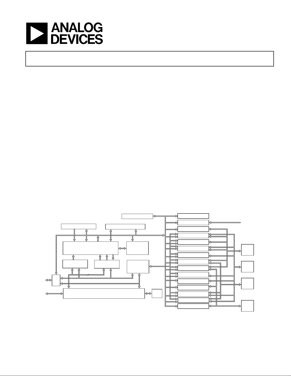
Figure 1. Processor Block Diagram
One Technology Way, P.O. Box 9106, Norwood, MA 02062-9106 U.S.A.
Tel: 781.329.4700 www.analog.com
Fax: 781.461.3113 © 2012 Analog Devices, Inc. All rights reserved.

ADSP-BF522/ADSP-BF523/ADSP-BF524/ADSP-BF525/ADSP-BF526/ADSP-BF527
TABLE OF CONTENTS
Features ................................................................. 1
Memory ................................................................ 1
Peripherals ............................................................. 1
General Description ................................................. 3
Portable Low Power Architecture ............................. 3
System Integration ................................................ 3
Processor Peripherals ............................................. 3
Blackfin Processor Core .......................................... 4
Memory Architecture ............................................ 5
DMA Controllers .................................................. 9
Host DMA Port .................................................... 9
Real-Time Clock ................................................. 10
Watchdog Timer ................................................ 10
Timers ............................................................. 10
Up/Down Counter and Thumbwheel Interface .......... 10
Serial Ports ........................................................ 11
Serial Peripheral Interface (SPI) Port ....................... 11
UART Ports ...................................................... 11
TWI Controller Interface ...................................... 12
10/100 Ethernet MAC .......................................... 12
Ports ................................................................ 12
Parallel Peripheral Interface (PPI) ........................... 13
USB On-The-Go Dual-Role Device Controller ........... 14
Code Security with Lockbox Secure Technology ......... 14
Dynamic Power Management ................................ 14
ADSP-BF523/ADSP-BF525/ADSP-BF527
Voltage Regulation ........................................... 16
ADSP-BF522/ADSP-BF524/ADSP-BF526
Voltage Regulation ........................................... 16
Clock Signals ..................................................... 16
Booting Modes ................................................... 18
Instruction Set Description .................................... 20
Development Tools .............................................. 21
Designing an Emulator-Compatible
Processor Board (Target) ................................... 21
Related Documents .............................................. 21
Related Signal Chains ........................................... 21
Lockbox Secure Technology Disclaimer .................... 21
Signal Descriptions ................................................. 22
Specifications ........................................................ 27
Operating Conditions
for ADSP-BF522/ADSP-BF524/ADSP-BF526
Processors ...................................................... 27
Operating Conditions
for ADSP-BF523/ADSP-BF525/ADSP-BF527
Processors ...................................................... 29
Electrical Characteristics ....................................... 31
Absolute Maximum Ratings ................................... 36
Package Information ............................................ 37
ESD Sensitivity ................................................... 37
Timing Specifications ........................................... 38
Output Drive Currents ......................................... 72
Test Conditions .................................................. 74
Environmental Conditions .................................... 78
289-Ball CSP_BGA Ball Assignment .. ......................... 79
208-Ball CSP_BGA Ball Assignment .. ......................... 82
Outline Dimensions ................................................ 85
Surface-Mount Design .......................................... 86
Automotive Products .............................................. 86
Ordering Guide ..................................................... 87
REVISION HISTORY
3/12—Rev. B to Rev. C
Corrected USB_VREF and USB_VBUS function (DOC ID:
DOC-881) descriptions in Signal Descriptions .............. 22
Corrected footnote on V
ADSP-BF523/ADSP-BF525/ADSP-BF527 Processors ..... 29
Corrected footnotes and added parameters (DOC-ID:
DOC-901 in Table 26, Absolute Maximum Ratings ........ 36
Corrected footnote on Table 27, Maximum Duty Cycle for
Input Transient Voltage, .......................................... 36
Added Table 29, Maximum Duty Cycle for IOH/IOL Current
Per Pin Group ....................................................... 37
, Operating Conditions for
DDMEM
Rev. C | Page 2 of 88 | March 2012
Replaced 289-Ball CSP_BGA (BC-289-2) ..................... 85
Added the ADBF525WYBCZxxx model to Automotive Prod-
ucts ..................................................................... 86
Added the ADSP-BF525ABCZ-5 and ADSP-BF525ABCZ-6
models to Ordering Guide ........................................ 87

ADSP-BF522/ADSP-BF523/ADSP-BF524/ADSP-BF525/ADSP-BF526/ADSP-BF527
GENERAL DESCRIPTION
The ADSP-BF52x processors are members of the Blackfin family of products, incorporating the Analog Devices/Intel Micro
Signal Architecture (MSA). Blackfin
®
processors combine a
dual-MAC state-of-the-art signal processing engine, the advantages of a clean, orthogonal RISC-like microprocessor
instruction set, and single-instruction, multiple-data (SIMD)
multimedia capabilities into a single instruction-set
architecture.
The ADSP-BF52x processors are completely code compatible
with other Blackfin processors. The ADSP-BF523/
ADSP-BF525/ADSP-BF527 processors offer performance up to
600 MHz. The ADSP-BF522/ADSP-BF524/ADSP-BF526 processors offer performance up to 400 MHz and reduced static
power consumption. Differences with respect to peripheral
combinations are shown in Table 1.
Table 1. Processor Comparison
Feature
Host DMA 111111
USB – 1 1 – 1 1
Ethernet MAC – – 1 – – 1
Internal Voltage Regulator – – – 1 1 1
TWI 111111
SPORTs 222222
UARTs 222222
SPI 111111
GP Timers 888888
GP Counter 111111
Watchdog Timers 111111
RTC 111111
Parallel Peripheral Interface 111111
GPIOs 48 48 48 48 48 48
L1 Instruction SRAM 48K 48K 48K 48K 48K 48K
L1 Instruction SRAM/Cache 16K 16K 16K 16K 16K 16K
L1 Data SRAM 32K 32K 32K 32K 32K 32K
L1 Data SRAM/Cache 32K 32K 32K 32K 32K 32K
L1 Scratchpad 4K 4K 4K 4K 4K 4K
Memory (bytes)
L3 Boot ROM 32K 32K 32K 32K 32K 32K
Maximum Instruction Rate
Maximum System Clock Speed 100 MHz 133 MHz
Package Options 289-Ball CSP_BGA
1
Maximum instruction rate is not available with every possible SCLK selection.
1
ADSP-BF522
ADSP-BF524
ADSP-BF526
ADSP-BF523
ADSP-BF525
400 MHz 600 MHz
208-Ball CSP_BGA
ADSP-BF527
By integrating a rich set of industry-leading system peripherals
and memory, Blackfin processors are the platform of choice for
next-generation applications that require RISC-like programmability, multimedia support, and leading-edge signal
processing in one integrated package.
PORTABLE LOW POWER ARCHITECTURE
Blackfin processors provide world-class power management
and performance. They are produced with a low power and low
voltage design methodology and feature on-chip dynamic
power management, which is the ability to vary both the voltage
and frequency of operation to significantly lower overall power
consumption. This capability can result in a substantial reduction in power consumption, compared with just varying the
frequency of operation. This allows longer battery life for
portable appliances.
SYSTEM INTEGRATION
The ADSP-BF52x processors are highly integrated system-on-achip solutions for the next generation of embedded network
connected applications. By combining industry-standard interfaces with a high performance signal processing core, costeffective applications can be developed quickly, without the
need for costly external components. The system peripherals
include an IEEE-compliant 802.3 10/100 Ethernet MAC, a USB
2.0 high speed OTG controller, a TWI controller, a NAND flash
controller, two UART ports, an SPI port, two serial ports
(SPORTs), eight general purpose 32-bit timers with PWM capability, a core timer, a real-time clock, a watchdog timer, a Host
DMA (HOSTDP) interface, and a parallel peripheral interface
(PPI).
PROCESSOR PERIPHERALS
The ADSP-BF52x processors contain a rich set of peripherals
connected to the core via several high bandwidth buses, providing flexibility in system configuration as well as excellent overall
system performance (see the block diagram on Page 1).
These Blackfin processors contain dedicated network communication modules and high speed serial and parallel ports, an
interrupt controller for flexible management of interrupts from
the on-chip peripherals or external sources, and power management control functions to tailor the performance and power
characteristics of the processor and system to many application
scenarios.
All of the peripherals, except for the general-purpose I/O, TWI,
real-time clock, and timers, are supported by a flexible DMA
structure. There are also separate memory DMA channels dedicated to data transfers between the processor's various memory
spaces, including external SDRAM and asynchronous memory.
Multiple on-chip buses running at up to 133 MHz provide
enough bandwidth to keep the processor core running along
with activity on all of the on-chip and external peripherals.
The ADSP-BF523/ADSP-BF525/ADSP-BF527 processors
include an on-chip voltage regulator in support of the processor’s dynamic power management capability. The voltage
Rev. C | Page 3 of 88 | March 2012
ADSP-BF522/ADSP-BF523/ADSP-BF524/ADSP-BF525/ADSP-BF526/ADSP-BF527
SEQUENCER
ALIGN
DECODE
LOOP BUFFER
16
16
8888
40 40
A0 A1
BARREL
SHIFTER
DATA ARITHMETIC UNIT
CONTROL
UNIT
R7.H
R6.H
R5.H
R4.H
R3.H
R2.H
R1.H
R0.H
R7.L
R6.L
R5.L
R4.L
R3.L
R2.L
R1.L
R0.L
AS TAT
40 40
32
32
32
32
32
32
32LD0
LD1
SD
DAG0
DAG1
ADDRESS ARITHMETIC UNIT
I3
I2
I1
I0
L3
L2
L1
L0
B3
B2
B1
B0
M3
M2
M1
M0
SP
FP
P5
P4
P3
P2
P1
P0
DA1
DA0
32
32
32
PREG
RAB
32
TO MEMORY
regulator provides a range of core voltage levels when supplied
from V
. The voltage regulator can be bypassed at the user's
DDEXT
discretion.
BLACKFIN PROCESSOR CORE
As shown in Figure 2, the Blackfin processor core contains two
16-bit multipliers, two 40-bit accumulators, two 40-bit ALUs,
four video ALUs, and a 40-bit shifter. The computation units
process 8-, 16-, or 32-bit data from the register file.
The compute register file contains eight 32-bit registers. When
performing compute operations on 16-bit operand data, the
register file operates as 16 independent 16-bit registers. All
operands for compute operations come from the multiported
register file and instruction constant fields.
Each MAC can perform a 16-bit by 16-bit multiply in each
cycle, accumulating the results into the 40-bit accumulators.
Signed and unsigned formats, rounding, and saturation
are supported.
The ALUs perform a traditional set of arithmetic and logical
operations on 16-bit or 32-bit data. In addition, many special
instructions are included to accelerate various signal processing
tasks. These include bit operations such as field extract and population count, modulo 232 multiply, divide primitives, saturation
and rounding, and sign/exponent detection. The set of video
instructions include byte alignment and packing operations,
16-bit and 8-bit adds with clipping, 8-bit average operations,
and 8-bit subtract/absolute value/accumulate (SAA) operations.
Also provided are the compare/select and vector search
instructions.
For certain instructions, two 16-bit ALU operations can be performed simultaneously on register pairs (a 16-bit high half and
16-bit low half of a compute register). If the second ALU is used,
quad 16-bit operations are possible.
Figure 2. Blackfin Processor Core
The 40-bit shifter can perform shifts and rotates and is used to
support normalization, field extract, and field deposit
instructions.
The program sequencer controls the flow of instruction execution, including instruction alignment and decoding. For
program flow control, the sequencer supports PC relative and
indirect conditional jumps (with static branch prediction), and
subroutine calls. Hardware is provided to support zero-overhead looping. The architecture is fully interlocked, meaning that
the programmer need not manage the pipeline when executing
instructions with data dependencies.
The address arithmetic unit provides two addresses for simultaneous dual fetches from memory. It contains a multiported
register file consisting of four sets of 32-bit index, modify,
Rev. C | Page 4 of 88 | March 2012
RESERVED
CORE MMR REGISTERS (2M BYTES)
RESERVED
SCRATCHPAD SRAM (4K BYTES)
INSTRUCTION BANK B SRAM (16K BYTES)
SYSTEM MMR RE GISTERS (2M BYTES)
RESERVED
RESERVED
DATA BANK B SRAM / CACHE (16K BYTES)
DATA BANK B SRAM (16K BYTES)
DATA BANK A SRAM / CACHE (16K BYTES)
ASYNC MEMORY BANK 3 (1M BYTES)
ASYNC MEMORY BANK 2 (1M BYTES)
ASYNC MEMORY BANK 1 ( 1M BYTES)
ASYNC MEMORY BANK 0 ( 1M BYTES)
SDRAM MEMORY (16M BYTES 128M BYTES)
INSTRUCTION SRAM / CACHE (16K BYTES)
IN
T
ER
N
A
L
M
EM
O
R
Y
M
AP
E
X
TE
R
NA
L
M
E
M
O
R
Y
M
A
P
0xFFFF FFFF
0xFFE0 0000
0xFFB0 0000
0xFFA1 4000
0xFFA1 0000
0xFF90 8000
0xFF90 4000
0xFF80 8000
0xFF80 4000
0x2040 0000
0x2030 0000
0x2020 0000
0x2010 0000
0x2000 0000
0xEF00 0000
0x0000 0000
0xFFC0 0000
0xFFB0 1000
0xFFA0 0000
DATA BANK A SRAM (16K BYTES)
0xFF90 0000
0xFF80 0000
RESERVED
RESERVED
0xFFA0 C000
0xFFA0 8000
INSTRUCTION BANK A SRAM (32K BYTES)
RESERVED
BOOT ROM (32K BYTES)
0xEF00 8000
RESERVED
0x08 00 0000
ADSP-BF522/ADSP-BF523/ADSP-BF524/ADSP-BF525/ADSP-BF526/ADSP-BF527
length, and base registers (for circular buffering), and eight
additional 32-bit pointer registers (for C-style indexed stack
manipulation).
Blackfin processors support a modified Harvard architecture in
combination with a hierarchical memory structure. Level 1 (L1)
memories are those that typically operate at the full processor
speed with little or no latency. At the L1 level, the instruction
memory holds instructions only. The two data memories hold
data, and a dedicated scratchpad data memory stores stack and
local variable information.
In addition, multiple L1 memory blocks are provided, offering a
configurable mix of SRAM and cache. The memory management unit (MMU) provides memory protection for individual
tasks that may be operating on the core and can protect system
registers from unintended access.
The architecture provides three modes of operation: user mode,
supervisor mode, and emulation mode. User mode has
restricted access to certain system resources, thus providing a
protected software environment, while supervisor mode has
unrestricted access to the system and core resources.
The Blackfin processor instruction set has been optimized so
that 16-bit opcodes represent the most frequently used instructions, resulting in excellent compiled code density. Complex
DSP instructions are encoded into 32-bit opcodes, representing
fully featured multifunction instructions. Blackfin processors
support a limited multi-issue capability, where a 32-bit instruction can be issued in parallel with two 16-bit instructions,
allowing the programmer to use many of the core resources in a
single instruction cycle.
The Blackfin processor assembly language uses an algebraic syntax for ease of coding and readability. The architecture has been
optimized for use in conjunction with the C/C++ compiler,
resulting in fast and efficient software implementations.
MEMORY ARCHITECTURE
The Blackfin processor views memory as a single unified
4G byte address space, using 32-bit addresses. All resources,
including internal memory, external memory, and I/O control
registers, occupy separate sections of this common address
space. The memory portions of this address space are arranged
in a hierarchical structure to provide a good cost/performance
balance of some very fast, low-latency on-chip memory as cache
or SRAM, and larger, lower-cost and performance off-chip
memory systems. See Figure 3.
The on-chip L1 memory system is the highest-performance
memory available to the Blackfin processor. The off-chip
memory system, accessed through the external bus interface
unit (EBIU), provides expansion with SDRAM, flash memory,
and SRAM, optionally accessing up to 132M bytes of
physical memory.
The memory DMA controller provides high-bandwidth datamovement capability. It can perform block transfers of code
or data between the internal memory and the external
memory spaces.
Rev. C | Page 5 of 88 | March 2012
Internal (On-Chip) Memory
The processor has three blocks of on-chip memory providing
high-bandwidth access to the core.
The first block is the L1 instruction memory, consisting of
64K bytes SRAM, of which 16K bytes can be configured as a
four-way set-associative cache. This memory is accessed at full
processor speed.
The second on-chip memory block is the L1 data memory, consisting of up to two banks of up to 32K bytes each. Each memory
bank is configurable, offering both cache and SRAM functionality. This memory block is accessed at full processor speed.
The third memory block is a 4K byte scratchpad SRAM which
runs at the same speed as the L1 memories, but is only accessible
as data SRAM and cannot be configured as cache memory.
External (Off-Chip) Memory
External memory is accessed via the EBIU. This 16-bit interface
provides a glueless connection to a bank of synchronous DRAM
(SDRAM), as well as up to four banks of asynchronous memory
devices including flash, EPROM, ROM, SRAM, and memory
mapped I/O devices.
Figure 3. Internal/External Memory Map

ADSP-BF522/ADSP-BF523/ADSP-BF524/ADSP-BF525/ADSP-BF526/ADSP-BF527
The SDRAM controller can be programmed to interface to up
to 128M bytes of SDRAM. A separate row can be open for each
SDRAM internal bank and the SDRAM controller supports up
to 4 internal SDRAM banks, improving overall performance.
The asynchronous memory controller can be programmed to
control up to four banks of devices with very flexible timing
requirements for a wide variety of devices. Each bank occupies a
1M byte segment regardless of the size of the devices used, so
that these banks are only contiguous if each is fully populated
with 1M byte of memory.
NAND Flash Controller (NFC)
The ADSP-BF52x processors provide a NAND flash controller
(NFC). NAND flash devices provide high-density, low-cost
memory. However, NAND flash devices also have long random
access times, invalid blocks, and lower reliability over device
lifetimes. Because of this, NAND flash is often used for readonly code storage. In this case, all DSP code can be stored in
NAND flash and then transferred to a faster memory (such as
SDRAM or SRAM) before execution. Another common use of
NAND flash is for storage of multimedia files or other large data
segments. In this case, a software file system may be used to
manage reading and writing of the NAND flash device. The file
system selects memory segments for storage with the goal of
avoiding bad blocks and equally distributing memory accesses
across all address locations. Hardware features of the NFC
include:
• Support for page program, page read, and block erase of
NAND flash devices, with accesses aligned to page
boundaries.
• Error checking and correction (ECC) hardware that facilitates error detection and correction.
• A single 8-bit external bus interface for commands,
addresses, and data.
• Support for SLC (single level cell) NAND flash devices
unlimited in size, with page sizes of 256 and 512 bytes.
Larger page sizes can be supported in software.
• Capability of releasing external bus interface pins during
long accesses.
• Support for internal bus requests of 16 bits.
• DMA engine to transfer data between internal mem ory a nd
NAND flash device.
One-Time Programmable Memory
The processor has 64K bits of one-time programmable nonvolatile memory that can be programmed by the developer only
one time. It includes the array and logic to support read access
and programming. Additionally, its pages can be write
protected.
OTP enables developers to store both public and private data
on-chip. In addition to storing public and private key data for
applications requiring security, it also allows developers to store
completely user-definable data such as customer ID, product
ID, MAC address, etc. Hence, generic parts can be shipped,
which are then programmed and protected by the developer
within this non-volatile memory.
I/O Memory Space
The processor does not define a separate I/O space. All
resources are mapped through the flat 32-bit address space.
On-chip I/O devices have their control registers mapped into
memory-mapped registers (MMRs) at addresses near the top of
the 4G byte address space. These are separated into two smaller
blocks, one which contains the control MMRs for all core functions, and the other which contains the registers needed for
setup and control of the on-chip peripherals outside of the core.
The MMRs are accessible only in supervisor mode and appear
as reserved space to on-chip peripherals.
Booting
The processor contains a small on-chip boot kernel, which configures the appropriate peripheral for booting. If the processor is
configured to boot from boot ROM memory space, the processor starts executing from the on-chip boot ROM. For more
information, see Booting Modes on Page 18.
Event Handling
The event controller on the processor handles all asynchronous
and synchronous events to the processor. The processor provides event handling that supports both nesting and
prioritization. Nesting allows multiple event service routines to
be active simultaneously. Prioritization ensures that servicing of
a higher-priority event takes precedence over servicing of a
lower-priority event. The controller provides support for five
different types of events:
• Emulation — An emulation event causes the processor to
enter emulation mode, allowing command and control of
the processor via the JTAG interface.
• RESET
• Nonmaskable Interrupt (NMI) — The NMI event can be
• Exceptions — Events that occur synchronously to program
• Interrupts — Events that occur asynchronously to program
Each event type has an associated register to hold the return
address and an associated return-from-event instruction. When
an event is triggered, the state of the processor is saved on the
supervisor stack.
The processor event controller consists of two stages, the core
event controller (CEC) and the system interrupt controller
(SIC). The core event controller works with the system interrupt
— This event resets the processor.
generated by the software watchdog timer or by the NMI
input signal to the processor. The NMI event is frequently
used as a power-down indicator to initiate an orderly shutdown of the system.
flow (in other words, the exception is taken before the
instruction is allowed to complete). Conditions such as
data alignment violations and undefined instructions cause
exceptions.
flow. They are caused by input signals, timers, and other
peripherals, as well as by an explicit software instruction.
Rev. C | Page 6 of 88 | March 2012
ADSP-BF522/ADSP-BF523/ADSP-BF524/ADSP-BF525/ADSP-BF526/ADSP-BF527
controller to prioritize and control all system events. Conceptually, interrupts from the peripherals enter into the SIC and are
then routed directly into the general-purpose interrupts of the
CEC.
Core Event Controller (CEC)
The CEC supports nine general-purpose interrupts (IVG15–7),
in addition to the dedicated interrupt and exception events. Of
these general-purpose interrupts, the two lowest-priority
interrupts (IVG15–14) are recommended to be reserved for
software interrupt handlers, leaving seven prioritized interrupt
inputs to support the peripherals of the processor. Table 2
describes the inputs to the CEC, identifies their names in the
event vector table (EVT), and lists their priorities.
System Interrupt Controller (SIC)
The system interrupt controller provides the mapping and routing of events from the many peripheral interrupt sources to the
prioritized general-purpose interrupt inputs of the CEC.
Although the processor provides a default mapping, the user
can alter the mappings and priorities of interrupt events by writing the appropriate values into the interrupt assignment
registers (SIC_IARx). Table 3 describes the inputs into the SIC
and the default mappings into the CEC.
Table 3. System Interrupt Controller (SIC)
Table 2. Core Event Controller (CEC)
Priority
(0 is Highest) Event Class EVT Entry
0Emulation/Test ControlEMU
1RESET
2 Nonmaskable Interrupt NMI
3Exception EVX
4 Reserved —
5 Hardware Error IVHW
6 Core Timer IVTMR
7 General-Purpose Interrupt 7 IVG7
8 General-Purpose Interrupt 8 IVG8
9 General-Purpose Interrupt 9 IVG9
10 General-Purpose Interrupt 10 IVG10
11 General-Purpose Interrupt 11 IVG11
12 General-Purpose Interrupt 12 IVG12
13 General-Purpose Interrupt 13 IVG13
14 General-Purpose Interrupt 14 IVG14
15 General-Purpose Interrupt 15 IVG15
RST
General Purpose
Peripheral Interrupt Event
PLL Wakeup Interrupt IVG7 0 0 IAR0 IMASK0, ISR0, IWR0
DMA Error 0 (generic) IVG7 1 0 IAR0 IMASK0, ISR0, IWR0
DMAR0 Block Interrupt IVG7 2 0 IAR0 IMASK0, ISR0, IWR0
DMAR1 Block Interrupt IVG7 3 0 IAR0 IMASK0, ISR0, IWR0
DMAR0 Overflow Error IVG7 4 0 IAR0 IMASK0, ISR0, IWR0
DMAR1 Overflow Error IVG7 5 0 IAR0 IMASK0, ISR0, IWR0
PPI Error IVG7 6 0 IAR0 IMASK0, ISR0, IWR0
MAC Status IVG7 7 0 IAR0 IMASK0, ISR0, IWR0
SPORT0 Status IVG7 8 0 IAR1 IMASK0, ISR0, IWR0
SPORT1 Status IVG7 9 0 IAR1 IMASK0, ISR0, IWR0
Reserved IVG7 10 0 IAR1 IMASK0, ISR0, IWR0
Reserved IVG7 11 0 IAR1 IMASK0, ISR0, IWR0
UART0 Status IVG7 12 0 IAR1 IMASK0, ISR0, IWR0
UART1 Status IVG7 13 0 IAR1 IMASK0, ISR0, IWR0
RTC IVG8 14 1 IAR1 IMASK0, ISR0, IWR0
DMA Channel 0 (PPI/NFC) IVG8 15 1 IAR1 IMASK0, ISR0, IWR0
DMA Channel 3 (SPORT0 RX) IVG9 16 2 IAR2 IMASK0, ISR0, IWR0
DMA Channel 4 (SPORT0 TX) IVG9 17 2 IAR2 IMASK0, ISR0, IWR0
DMA Channel 5 (SPORT1 RX) IVG9 18 2 IAR2 IMASK0, ISR0, IWR0
DMA Channel 6 (SPORT1 TX) IVG9 19 2 IAR2 IMASK0, ISR0, IWR0
TWI IVG10 20 3 IAR2 IMASK0, ISR0, IWR0
DMA Channel 7 (SPI) IVG10 21 3 IAR2 IMASK0, ISR0, IWR0
DMA Channel 8 (UART0 RX) IVG10 22 3 IAR2 IMASK0, ISR0, IWR0
DMA Channel 9 (UART0 TX) IVG10 23 3 IAR2 IMASK0, ISR0, IWR0
DMA Channel 10 (UART1 RX) IVG10 24 3 IAR3 IMASK0, ISR0, IWR0
DMA Channel 11 (UART1 TX) IVG10 25 3 IAR3 IMASK0, ISR0, IWR0
Interrupt (at RESET)Peripheral Interrupt ID
Default
Core Interrupt ID
SIC Registers
Rev. C | Page 7 of 88 | March 2012

ADSP-BF522/ADSP-BF523/ADSP-BF524/ADSP-BF525/ADSP-BF526/ADSP-BF527
Table 3. System Interrupt Controller (SIC) (Continued)
General Purpose
Peripheral Interrupt Event
OTP Memory Interrupt IVG11 26 4 IAR3 IMASK0, ISR0, IWR0
GP Counter IVG11 27 4 IAR3 IMASK0, ISR0, IWR0
DMA Channel 1 (MAC RX/HOSTDP) IVG11 28 4 IAR3 IMASK0, ISR0, IWR0
Port H Interrupt A IVG11 29 4 IAR3 IMASK0, ISR0, IWR0
DMA Channel 2 (MAC TX/NFC) IVG11 30 4 IAR3 IMASK0, ISR0, IWR0
Port H Interrupt B IVG11 31 4 IAR3 IMASK0, ISR0, IWR0
Timer 0 IVG12 32 5 IAR4 IMASK1, ISR1, IWR1
Timer 1 IVG12 33 5 IAR4 IMASK1, ISR1, IWR1
Timer 2 IVG12 34 5 IAR4 IMASK1, ISR1, IWR1
Timer 3 IVG12 35 5 IAR4 IMASK1, ISR1, IWR1
Timer 4 IVG12 36 5 IAR4 IMASK1, ISR1, IWR1
Timer 5 IVG12 37 5 IAR4 IMASK1, ISR1, IWR1
Timer 6 IVG12 38 5 IAR4 IMASK1, ISR1, IWR1
Timer 7 IVG12 39 5 IAR4 IMASK1, ISR1, IWR1
Port G Interrupt A IVG12 40 5 IAR5 IMASK1, ISR1, IWR1
Port G Interrupt B IVG12 41 5 IAR5 IMASK1, ISR1, IWR1
MDMA Stream 0 IVG13 42 6 IAR5 IMASK1, ISR1, IWR1
MDMA Stream 1 IVG13 43 6 IAR5 IMASK1, ISR1, IWR1
Software Watchdog Timer IVG13 44 6 IAR5 IMASK1, ISR1, IWR1
Port F Interrupt A IVG13 45 6 IAR5 IMASK1, ISR1, IWR1
Port F Interrupt B IVG13 46 6 IAR5 IMASK1, ISR1, IWR1
SPI Status IVG7 47 0 IAR5 IMASK1, ISR1, IWR1
NFC Status IVG7 48 0 IAR6 IMASK1, ISR1, IWR1
HOSTDP Status IVG7 49 0 IAR6 IMASK1, ISR1, IWR1
Host Read Done IVG7 50 0 IAR6 IMASK1, ISR1, IWR1
Reserved IVG10 51 3 IAR6 IMASK1, ISR1, IWR1
USB_INT0 Interrupt IVG10 52 3 IAR6 IMASK1, ISR1, IWR1
USB_INT1 Interrupt IVG10 53 3 IAR6 IMASK1, ISR1, IWR1
USB_INT2 Interrupt IVG10 54 3 IAR6 IMASK1, ISR1, IWR1
USB_DMAINT Interrupt IVG10 55 3 IAR6 IMASK1, ISR1, IWR1
Interrupt (at RESET)Peripheral Interrupt ID
Default
Core Interrupt ID
SIC Registers
Event Control
The processor provides a very flexible mechanism to control the
processing of events. In the CEC, three registers are used to
coordinate and control events. Each register is 16 bits wide.
• CEC interrupt latch register (ILAT) — Indicates when
events have been latched. The appropriate bit is set when
the processor has latched the event and cleared when the
event has been accepted into the system. This register is
updated automatically by the controller, but it may be written only when its corresponding IMASK bit is cleared.
• CEC interrupt mask register (IMASK) — Controls the
masking and unmasking of individual events. When a bit is
set in the IMASK register, that event is unmasked and is
processed by the CEC when asserted. A cleared bit in the
IMASK register masks the event, preventing the processor
from servicing the event even though the event may be
latched in the ILAT register. This register may be read or
Rev. C | Page 8 of 88 | March 2012
written while in supervisor mode. (Note that generalpurpose interrupts can be globally enabled and disabled
with the STI and CLI instructions, respectively.)
• CEC interrupt pending register (IPEND) — The IPEND
register keeps track of all nested events. A set bit in the
IPEND register indicates the event is currently active or
nested at some level. This register is updated automatically
by the controller but may be read while in supervisor mode.
The SIC allows further control of event processing by providing
three pairs of 32-bit interrupt control and status registers. Each
register contains a bit corresponding to each of the peripheral
interrupt events shown in Table 3 on Page 7.
• SIC interrupt mask registers (SIC_IMASKx) — Control the
masking and unmasking of each peripheral interrupt event.
When a bit is set in these registers, that peripheral event is

ADSP-BF522/ADSP-BF523/ADSP-BF524/ADSP-BF525/ADSP-BF526/ADSP-BF527
unmasked and is processed by the system when asserted. A
cleared bit in the register masks the peripheral event, preventing the processor from servicing the event.
• SIC interrupt status registers (SIC_ISRx) — As multiple
peripherals can be mapped to a single event, these registers
allow the software to determine which peripheral event
source triggered the interrupt. A set bit indicates the
peripheral is asserting the interrupt, and a cleared bit indicates the peripheral is not asserting the event.
• SIC interrupt wakeup enable registers (SIC_IWRx) — By
enabling the corresponding bit in these registers, a peripheral can be configured to wake up the processor, should the
core be idled or in sleep mode when the event is generated.
For more information see Dynamic Power Management on
Page 14.
Because multiple interrupt sources can map to a single generalpurpose interrupt, multiple pulse assertions can occur simultaneously, before or during interrupt processing for an interrupt
event already detected on this interrupt input. The IPEND
register contents are monitored by the SIC as the interrupt
acknowledgement.
The appropriate ILAT register bit is set when an interrupt rising
edge is detected (detection requires two core clock cycles). The
bit is cleared when the respective IPEND register bit is set. The
IPEND bit indicates that the event has entered into the processor pipeline. At this point the CEC recognizes and queues the
next rising edge event on the corresponding event input. The
minimum latency from the rising edge transition of the generalpurpose interrupt to the IPEND output asserted is three core
clock cycles; however, the latency can be much higher, depending on the activity within and the state of the processor.
DMA CONTROLLERS
The processor has multiple, independent DMA channels that
support automated data transfers with minimal overhead for
the processor core. DMA transfers can occur between the
processor's internal memories and any of its DMA-capable
peripherals. Additionally, DMA transfers can be accomplished
between any of the DMA-capable peripherals and external
devices connected to the external memory interfaces, including
the SDRAM controller and the asynchronous memory controller. DMA-capable peripherals include the Ethernet MAC, NFC,
HOSTDP, USB, SPORTs, SPI port, UARTs, and PPI. Each individual DMA-capable peripheral has at least one dedicated DMA
channel.
The processor DMA controller supports both one-dimensional
(1-D) and two-dimensional (2-D) DMA transfers. DMA transfer initialization can be implemented from registers or from sets
of parameters called descriptor blocks.
The 2-D DMA capability supports arbitrary row and column
sizes up to 64K elements by 64K elements, and arbitrary row
and column step sizes up to ±32K elements. Furthermore, the
column step size can be less than the row step size, allowing
implementation of interleaved data streams. This feature is
especially useful in video applications where data can be deinterleaved on the fly.
Examples of DMA types supported by the processor DMA controller include:
• A single, linear buffer that stops upon completion.
• A circular, auto-refreshing buffer that interrupts on each
full or fractionally full buffer.
• 1-D or 2-D DMA using a linked list of descriptors.
• 2-D DMA using an array of descriptors, specifying only the
base DMA address within a common page.
In addition to the dedicated peripheral DMA channels, there are
two memory DMA channels provided for transfers between the
various memories of the processor system. This enables transfers of blocks of data between any of the memories—including
external SDRAM, ROM, SRAM, and flash memory—with minimal processor intervention. Memory DMA transfers can be
controlled by a very flexible descriptor-based methodology or
by a standard register-based autobuffer mechanism.
The processor also has an external DMA controller capability
via dual external DMA request pins when used in conjunction
with the external bus interface unit (EBIU). This functionality
can be used when a high speed interface is required for external
FIFOs and high bandwidth communications peripherals such as
USB 2.0. It allows control of the number of data transfers for
memory DMA. The number of transfers per edge is programmable. This feature can be programmed to allow memory
DMA to have an increased priority on the external bus relative
to the core.
HOST DMA PORT
The host port interface allows an external host to be a DMA
master to transfer data in and out of the device. The host device
masters the transactions and the Blackfin processor is the
DMA slave.
The host port is enabled through the PAB interface. Once
enabled, the DMA is controlled by the external host, which can
then program the DMA to send/receive data to any valid internal or external memory location.
The host port interface controller has the following features.
• Allows external master to configure DMA read/write data
transfers and read port status.
• Uses asynchronous memory protocol for external interface.
• 8-/16-bit external data interface to host device.
• Half duplex operation.
• Little-/big-endian data transfer.
• Acknowledge mode allows flow control on host
transactions.
• Interrupt mode guarantees a burst of FIFO depth host
transactions.
REAL-TIME CLOCK
The real-time clock (RTC) provides a robust set of digital watch
features, including current time, stopwatch, and alarm. The
RTC is clocked by a 32.768 kHz crystal external to the Blackfin
processor. Connect RTC pins RTXI and RTXO with external
Rev. C | Page 9 of 88 | March 2012

ADSP-BF522/ADSP-BF523/ADSP-BF524/ADSP-BF525/ADSP-BF526/ADSP-BF527
RTXO
C1 C2
X1
SUGGESTED COMPONENTS:
X1 = ECLIPTEK EC38J (THROUGH-HOLE PACKAGE) OR
EPSON MC405 12 pF LOAD (SURFACE-MOUNT PACKAGE)
C1 = 22 pF
C2 = 22 pF
R1 = 10 M:
NOTE: C1 AND C2 ARE SPECIFIC TO CRYSTAL SPECIFIED FOR X1.
CONTACT CRYSTAL MANUFACTURER FOR DETAILS. C1 AND C2
SPECIFICATIONS ASSUME BOARD TRACE CAPACITANCE OF 3 pF.
RTXI
R1
components as shown in Figure 4.
Figure 4. External Components for RTC
The RTC peripheral has dedicated power supply pins so that it
can remain powered up and clocked even when the rest of the
processor is in a low power state. The RTC provides several programmable interrupt options, including interrupt per second,
minute, hour, or day clock ticks, interrupt on programmable
stopwatch countdown, or interrupt at a programmed alarm
time.
The 32.768 kHz input clock frequency is divided down to a 1 Hz
signal by a prescaler. The counter function of the timer consists
of four counters: a 60-second counter, a 60-minute counter, a
24-hour counter, and an 32,768-day counter.
When enabled, the alarm function generates an interrupt when
the output of the timer matches the programmed value in the
alarm control register. There are two alarms: The first alarm is
for a time of day. The second alarm is for a day and time of
that day.
The stopwatch function counts down from a programmed
value, with one-second resolution. When the stopwatch is
enabled and the counter underflows, an interrupt is generated.
Like the other peripherals, the RTC can wake up the processor
from sleep mode upon generation of any RTC wake-up event.
Additionally, an RTC wakeup event can wake up the processor
from deep sleep mode or cause a transition from the hibernate
state.
WATCHDOG TIMER
The processor includes a 32-bit timer that can be used to implement a software watchdog function. A software watchdog can
improve system availability by forcing the processor to a known
state through generation of a hardware reset, nonmaskable
interrupt (NMI), or general-purpose interrupt, if the timer
expires before being reset by software. The programmer initializes the count value of the timer, enables the appropriate
interrupt, then enables the timer. Thereafter, the software must
reload the counter before it counts to zero from the programmed value. This protects the system from remaining in an
unknown state where software, which would normally reset the
timer, has stopped running due to an external noise condition
or software error.
If configured to generate a hardware reset, the watchdog timer
resets both the core and the processor peripherals. After a reset,
software can determine if the watchdog was the source of the
hardware reset by interrogating a status bit in the watchdog
timer control register.
The timer is clocked by the system clock (SCLK), at a maximum
frequency of f
TIMERS
There are nine general-purpose programmable timer units in
the processors. Eight timers have an external pin that can be
configured either as a pulse width modulator (PWM) or timer
output, as an input to clock the timer, or as a mechanism for
measuring pulse widths and periods of external events. These
timers can be synchronized to an external clock input to the several other associated PF pins, an external clock input to the
PPI_CLK input pin, or to the internal SCLK.
The timer units can be used in conjunction with the two UARTs
to measure the width of the pulses in the data stream to provide
a software auto-baud detect function for the respective serial
channels.
The timers can generate interrupts to the processor core providing periodic events for synchronization, either to the system
clock or to a count of external signals.
In addition to the eight general-purpose programmable timers,
a ninth timer is also provided. This extra timer is clocked by the
internal processor clock and is typically used as a system tick
clock for generation of operating system periodic interrupts.
UP/DOWN COUNTER AND THUMBWHEEL INTERFACE
A 32-bit up/down counter is provided that can sense 2-bit
quadrature or binary codes as typically emitted by industrial
drives or manual thumb wheels. The counter can also operate in
general-purpose up/down count modes. Then, count direction
is either controlled by a level-sensitive input pin or by two edge
detectors.
A third input can provide flexible zero marker support and can
alternatively be used to input the push-button signal of thumb
wheels. All three pins have a programmable debouncing circuit.
An internal signal forwarded to the timer unit enables one timer
to measure the intervals between count events. Boundary registers enable auto-zero operation or simple system warning by
interrupts when programmable count values are exceeded.
SERIAL PORTS
The processors incorporate two dual-channel synchronous
serial ports (SPORT0 and SPORT1) for serial and multiprocessor communications. The SPORTs support the following
features:
2
S capable operation.
•I
Rev. C | Page 10 of 88 | March 2012
SCLK
.

ADSP-BF522/ADSP-BF523/ADSP-BF524/ADSP-BF525/ADSP-BF526/ADSP-BF527
SPI Clock Rate
f
SCLK
2 SPI_BAUD×
----------------------------------- -
=
UART Clock Rate
f
SCLK
16 UART_Divisor×
-----------------------------------------------
=
• Bidirectional operation — Each SPORT has two sets of
independent transmit and receive pins, enabling eight
channels of I
2
S stereo audio.
• Buffered (8-deep) transmit and receive ports — Each port
has a data register for transferring data words to and from
other processor components and shift registers for shifting
data in and out of the data registers.
• Clocking — Each transmit and receive port can either use
an external serial clock or generate its own, in frequencies
ranging from (f
/131,070) Hz to (f
SCLK
SCLK
/2) Hz.
• Word length – Each SPORT supports serial data words
from 3 to 32 bits in length, transferred most-significant-bit
first or least-significant-bit first.
• Framing — Each transmit and receive port can run with or
without frame sync signals for each data word. Frame sync
signals can be generated internally or externally, active high
or low, and with either of two pulse widths and early or late
frame sync.
• Companding in hardware — Each SPORT can perform
A-law or µ-law companding according to ITU recommendation G.711. Companding can be selected on the transmit
and/or receive channel of the SPORT without
additional latencies.
• DMA operations with single-cycle overhead — Each
SPORT can automatically receive and transmit multiple
buffers of memory data. The processor can link or chain
sequences of DMA transfers between a SPORT and
memory.
• Interrupts — Each transmit and receive port generates an
interrupt upon completing the transfer of a data word or
after transferring an entire data buffer, or buffers,
through DMA.
• Multichannel capability — Each SPORT supports 128
channels out of a 1024-channel window and is compatible
with the H.100, H.110, MVIP-90, and HMVIP standards.
SERIAL PERIPHERAL INTERFACE (SPI) PORT
The processors have an SPI-compatible port that enables the
processor to communicate with multiple SPI-compatible
devices.
The SPI interface uses three pins for transferring data: two data
pins (Master Output-Slave Input, MOSI, and Master InputSlave Output, MISO) and a clock pin (serial clock, SCK). An SPI
chip select input pin (SPISS
processor, and seven SPI chip select output pins (SPISEL7–1
the processor select other SPI devices. The SPI select pins are
reconfigured general-purpose I/O pins. Using these pins, the
SPI port provides a full-duplex, synchronous serial interface,
which supports both master/slave modes and multimaster
environments.
The SPI port’s baud rate and clock phase/polarities are programmable, and it has an integrated DMA channel,
configurable to support transmit or receive data streams. The
SPI’s DMA channel can only service unidirectional accesses at
any given time.
) lets other SPI devices select the
) let
The SPI port’s clock rate is calculated as:
Where the 16-bit SPI_BAUD register contains a value of 2
to 65,535.
During transfers, the SPI port simultaneously transmits and
receives by serially shifting data in and out on its two serial data
lines. The serial clock line synchronizes the shifting and sampling of data on the two serial data lines.
UART PORTS
The processors provide two full-duplex universal asynchronous
receiver/transmitter (UART) ports, which are fully compatible
with PC-standard UARTs. Each UART port provides a simplified UART interface to other peripherals or hosts, supporting
full-duplex, DMA-supported, asynchronous transfers of serial
data. A UART port includes support for five to eight data bits,
one or two stop bits, and none, even, or odd parity. Each UART
port supports two modes of operation:
• PIO (programmed I/O) — The processor sends or receives
data by writing or reading I/O mapped UART registers.
The data is double-buffered on both transmit and receive.
• DMA (direct memory access) — The DMA controller
transfers both transmit and receive data. This reduces the
number and frequency of interrupts required to transfer
data to and from memory. The UART has two dedicated
DMA channels, one for transmit and one for receive. These
DMA channels have lower default priority than most DMA
channels because of their relatively low service rates.
Each UART port's baud rate, serial data format, error code generation and status, and interrupts are programmable:
• Supporting bit rates ranging from (f
/16) bits per second.
(f
SCLK
• Supporting data formats from seven to 12 bits per frame.
• Both transmit and receive operations can be configured to
generate maskable interrupts to the processor.
The UART port’s clock rate is calculated as:
Where the 16-bit UART_Divisor comes from the UART_DLH
(most significant 8 bits) and UART_DLL (least significant
8 bits) registers.
In conjunction with the general-purpose timer functions, autobaud detection is supported.
The capabilities of the UARTs are further extended with support for the infrared data association (IrDA®) serial infrared
physical layer link specification (SIR) protocol.
/1,048,576) to
SCLK
Rev. C | Page 11 of 88 | March 2012

ADSP-BF522/ADSP-BF523/ADSP-BF524/ADSP-BF525/ADSP-BF526/ADSP-BF527
TWI CONTROLLER INTERFACE
The processors include a 2-wire interface (TWI) module for
providing a simple exchange method of control data between
multiple devices. The TWI is compatible with the widely used
2C®
I
bus standard. The TWI module offers the capabilities of
simultaneous master and slave operation and support for both
7-bit addressing and multimedia data arbitration. The TWI
interface utilizes two pins for transferring clock (SCL) and data
(SDA) and supports the protocol at speeds up to 400k bits/sec.
The TWI interface pins are compatible with 5 V logic levels.
Additionally, the TWI module is fully compatible with serial
camera control bus (SCCB) functionality for easier control of
various CMOS camera sensor devices.
10/100 ETHERNET MAC
The ADSP-BF526 and ADSP-BF527 processors offer the capability to directly connect to a network by way of an embedded
Fast Ethernet Media Access Controller (MAC) that supports
both 10-BaseT (10M bits/sec) and 100-BaseT (100M bits/sec)
operation. The 10/100 Ethernet MAC peripheral on the processor is fully compliant to the IEEE 802.3-2002 standard and it
provides programmable features designed to minimize supervision, bus use, or message processing by the rest of the processor
system.
Some standard features are:
• Support of MII and RMII protocols for external PHYs.
• Full duplex and half duplex modes.
• Data framing and encapsulation: generation and detection
of preamble, length padding, and FCS.
• Media access management (in half-duplex operation): collision and contention handling, including control of
retransmission of collision frames and of back-off timing.
• Flow control (in full-duplex operation): generation and
detection of PAUSE frames.
• Station management: generation of MDC/MDIO frames
for read-write access to PHY registers.
• Operating range for active and sleep operating modes, see
Table 58 on Page 67 and Table 59 on Page 67.
• Internal loopback from Tx to Rx.
Some advanced features are:
• Buffered crystal output to external PHY for support of a
single crystal system.
• Automatic checksum computation of IP header and IP
payload fields of Rx frames.
• Independent 32-bit descriptor-driven Rx and Tx DMA
channels.
• Frame status delivery to memory via DMA, including
frame completion semaphores, for efficient buffer queue
management in software.
• Tx DMA support for separate descriptors for MAC header
and payload to eliminate buffer copy operations.
• Convenient frame alignment modes support even 32-bit
alignment of encapsulated Rx or Tx IP packet data in memory after the 14-byte MAC header.
• Programmable Ethernet event interrupt supports any combination of:
• Any selected Rx or Tx frame status conditions.
• PHY interrupt condition.
• Wake-up frame detected.
• Any selected MAC management counter(s) at halffull.
• DMA descriptor error.
• 47 MAC management statistics counters with selectable
clear-on-read behavior and programmable interrupts on
half maximum value.
• Programmable Rx address filters, including a 64-bin
address hash table for multicast and/or unicast frames, and
programmable filter modes for broadcast, multicast, unicast, control, and damaged frames.
• Advanced power management supporting unattended
transfer of Rx and Tx frames and status to/from external
memory via DMA during low power sleep mode.
• System wakeup from sleep operating mode upon magic
packet or any of four user-definable wakeup frame filters.
• Support for 802.3Q tagged VLAN frames.
• Programmable MDC clock rate and preamble suppression.
• In RMII operation, seven unused pins may be configured
as GPIO pins for other purposes.
PORTS
Because of the rich set of peripherals, the processor groups the
many peripheral signals to four ports—Port F, Port G, Port H,
and Port J. Most of the associated pins are shared by multiple
signals. The ports function as multiplexer controls.
General-Purpose I/O (GPIO)
The processor has 48 bidirectional, general-purpose I/O (GPIO)
pins allocated across three separate GPIO modules—PORTFIO,
PORTGIO, and PORTHIO, associated with Port F, Port G, and
Port H, respectively. Port J does not provide GPIO functionality. Each GPIO-capable pin shares functionality with other
processor peripherals via a multiplexing scheme; however, the
GPIO functionality is the default state of the device upon
power-up. Neither GPIO output nor input drivers are active by
default. Each general-purpose port pin can be individually controlled by manipulation of the port control, status, and interrupt
registers:
• GPIO direction control register — Specifies the direction of
each individual GPIO pin as input or output.
• GPIO control and status registers — The processor
employs a “write one to modify” mechanism that allows
any combination of individual GPIO pins to be modified in
a single instruction, without affecting the level of any other
GPIO pins. Four control registers are provided. One regis-
Rev. C | Page 12 of 88 | March 2012

ADSP-BF522/ADSP-BF523/ADSP-BF524/ADSP-BF525/ADSP-BF526/ADSP-BF527
ter is written in order to set pin values, one register is
written in order to clear pin values, one register is written
in order to toggle pin values, and one register is written in
order to specify a pin value. Reading the GPIO status register allows software to interrogate the sense of the pins.
• GPIO interrupt mask registers — The two GPIO interrupt
mask registers allow each individual GPIO pin to function
as an interrupt to the processor. Similar to the two GPIO
control registers that are used to set and clear individual
pin values, one GPIO interrupt mask register sets bits to
enable interrupt function, and the other GPIO interrupt
mask register clears bits to disable interrupt function.
GPIO pins defined as inputs can be configured to generate
hardware interrupts, while output pins can be triggered by
software interrupts.
• GPIO interrupt sensitivity registers — The two GPIO interrupt sensitivity registers specify whether individual pins are
level- or edge-sensitive and specify—if edge-sensitive—
whether just the rising edge or both the rising and falling
edges of the signal are significant. One register selects the
type of sensitivity, and one register selects which edges are
significant for edge-sensitivity.
PARALLEL PERIPHERAL INTERFACE (PPI)
The processor provides a parallel peripheral interface (PPI) that
can connect directly to parallel analog-to-digital and digital-toanalog converters, video encoders and decoders, and other general-purpose peripherals. The PPI consists of a dedicated input
clock pin, up to three frame synchronization pins, and up to 16
data pins. The input clock supports parallel data rates up to half
the system clock rate, and the synchronization signals can be
configured as either inputs or outputs.
The PPI supports a variety of general-purpose and ITU-R 656
modes of operation. In general-purpose mode, the PPI provides
half-duplex, bidirectional data transfer with up to 16 bits of
data. Up to three frame synchronization signals are also provided. In ITU-R 656 mode, the PPI provides half-duplex
bidirectional transfer of 8- or 10-bit video data. Additionally,
on-chip decode of embedded start-of-line (SOL) and start-offield (SOF) preamble packets is supported.
General-Purpose Mode Descriptions
The general-purpose modes of the PPI are intended to suit a
wide variety of data capture and transmission applications.
Three distinct submodes are supported:
1. Input mode — Frame syncs and data are inputs into the
PPI.
2. Frame capture mode — Frame syncs are outputs from the
PPI, but data are inputs.
3. Output mode — Frame syncs and data are outputs from
the PPI.
Input Mode
Input mode is intended for ADC applications, as well as video
communication with hardware signaling. In its simplest form,
PPI_FS1 is an external frame sync input that controls when to
read data. The PPI_DELAY MMR allows for a delay (in
PPI_CLK cycles) between reception of this frame sync and the
initiation of data reads. The number of input data samples is
user programmable and defined by the contents of the
PPI_COUNT register. The PPI supports 8-bit and 10-bit
through 16-bit data, programmable in the PPI_CONTROL
register.
Frame Capture Mode
Frame capture mode allows the video source(s) to act as a slave
(for frame capture for example). The ADSP-BF52x processors
control when to read from the video source(s). PPI_FS1 is an
HSYNC output, and PPI_FS2 is a VSYNC output.
Output Mode
Output mode is used for transmitting video or other data with
up to three output frame syncs. Typically, a single frame sync is
appropriate for data converter applications, whereas two or
three frame syncs could be used for sending video with hardware signaling.
ITU-R 656 Mode Descriptions
The ITU-R 656 modes of the PPI are intended to suit a wide
variety of video capture, processing, and transmission applications. Three distinct submodes are supported:
1. Active video only mode
2. Vertical blanking only mode
3. Entire field mode
Active Video Mode
Active video only mode is used when only the active video portion of a field is of interest and not any of the blanking intervals.
The PPI does not read in any data between the end of active
video (EAV) and start of active video (SAV) preamble symbols,
or any data present during the vertical blanking intervals. In this
mode, the control byte sequences are not stored to memory;
they are filtered by the PPI. After synchronizing to the start of
Field 1, the PPI ignores incoming samples until it sees an SAV
code. The user specifies the number of active video lines per
frame (in PPI_COUNT register).
Vertical Blanking Interval Mode
In this mode, the PPI only transfers vertical blanking interval
(VBI) data.
Entire Field Mode
In this mode, the entire incoming bit stream is read in through
the PPI. This includes active video, control preamble sequences,
and ancillary data that may be embedded in horizontal and vertical blanking intervals. Data transfer starts immediately after
synchronization to Field 1. Data is transferred to or from the
synchronous channels through eight DMA engines that work
autonomously from the processor core.
Rev. C | Page 13 of 88 | March 2012

ADSP-BF522/ADSP-BF523/ADSP-BF524/ADSP-BF525/ADSP-BF526/ADSP-BF527
USB ON-THE-GO DUAL-ROLE DEVICE CONTROLLER
The USB OTG dual-role device controller (USBDRC) provides
a low-cost connectivity solution for consumer mobile devices
such as cell phones, digital still cameras, and MP3 players,
allowing these devices to transfer data using a point-to-point
USB connection without the need for a PC host. The USBDRC
module can operate in a traditional USB peripheral-only mode
as well as the host mode presented in the On-the-Go (OTG)
supplement to the USB 2.0 specification. In host mode, the USB
module supports transfers at high speed (480 Mbps), full speed
(12 Mbps), and low speed (1.5 Mbps) rates. Peripheral-only
mode supports the high- and full-speed transfer rates.
The USB clock (USB_XI) is provided through a dedicated external crystal or crystal oscillator. See Universal Serial Bus (USB)
On-The-Go—Receive and Transmit Timing on Page 59 for
related timing requirements. If using a crystal to provide the
USB clock, use a parallel-resonant, fundamental mode, microprocessor-grade crystal.
The USB on-the-go dual-role device controller includes a phase
locked loop with programmable multipliers to generate the necessary internal clocking frequency for USB. The multiplier value
should be programmed based on the USB_XI frequency to
achieve the necessary 480 MHz internal clock for USB high
speed operation. For example, for a USB_XI crystal frequency of
24 MHz, the USB_PLLOSC_CTRL register should be programmed with a multiplier value of 20 to generate a 480 MHz
internal clock.
CODE SECURITY WITH LOCKBOX SECURE TE CH N O LO G Y
A security system consisting of a blend of hardware and software provides customers with a flexible and rich set of code
security features with Lockbox
tures include:
•OTP memory
• Unique chip ID
• Code authentication
• Secure mode of operation
The security scheme is based upon the concept of authentication of digital signatures using standards-based algorithms and
provides a secure processing environment in which to execute
code and protect assets. See Lockbox Secure Technology Dis-
claimer on Page 21.
TM
Secure Technology. Key fea-
DYNAMIC POWER MANAGEMENT
The processor provides five operating modes, each with a different performance/power profile. In addition, dynamic power
management provides the control functions to dynamically alter
the processor core supply voltage, further reducing power dissipation. When configured for a 0 V core supply voltage, the
processor enters the hibernate state. Control of clocking to each
of the processor peripherals also reduces power consumption.
See Table 4 for a summary of the power settings for each mode.
Table 4. Power Settings
Core
PLL
Mode/State PLL
Full-On Enabled No Enabled Enabled On
Active Enabled/
Disabled
Sleep Enabled — Disabled Enabled On
Deep Sleep Disabled — Disabled Disabled On
Hibernate Disabled — Disabled Disabled Off
Bypassed
Yes E na bl ed E na bl ed O n
Clock
(CCLK)
System
Clock
(SCLK)
Core
Power
Full-On Operating Mode—Maximum Performance
In the full-on mode, the PLL is enabled and is not bypassed,
providing capability for maximum operational frequency. This
is the power-up default execution state in which maximum performance can be achieved. The processor core and all enabled
peripherals run at full speed.
Active Operating Mode—Moderate Dynamic Power Savings
In the active mode, the PLL is enabled but bypassed. Because the
PLL is bypassed, the processor’s core clock (CCLK) and system
clock (SCLK) run at the input clock (CLKIN) frequency. DMA
access is available to appropriately configured L1 memories.
In the active mode, it is possible to disable the control input to
the PLL by setting the PLL_OFF bit in the PLL control register.
This register can be accessed with a user-callable routine in the
on-chip ROM called bfrom_SysControl(). If disabled, the PLL
control input must be re-enabled before transitioning to the
full-on or sleep modes.
For more information about PLL controls, see the “Dynamic
Power Management” chapter in the ADSP-BF52x Blackfin Processor Hardware Reference.
Sleep Operating Mode—High Dynamic Power Savings
The sleep mode reduces dynamic power dissipation by disabling
the clock to the processor core (CCLK). The PLL and system
clock (SCLK), however, continue to operate in this mode. Typically, an external event or RTC activity wakes up the processor.
When in the sleep mode, asserting a wakeup enabled in the
SIC_IWRx registers causes the processor to sense the value of
the BYPASS bit in the PLL control register (PLL_CTL). If
BYPASS is disabled, the processor transitions to the full-on
mode. If BYPASS is enabled, the processor transitions to the
active mode.
System DMA access to L1 memory is not supported in
sleep mode.
Deep Sleep Operating Mode—Maximum Dynamic Power Savings
The deep sleep mode maximizes dynamic power savings by disabling the clocks to the processor core (CCLK) and to all
synchronous peripherals (SCLK). Asynchronous peripherals,
Rev. C | Page 14 of 88 | March 2012

ADSP-BF522/ADSP-BF523/ADSP-BF524/ADSP-BF525/ADSP-BF526/ADSP-BF527
Power Savings Factor
f
CCLKRED
f
CCLKNOM
--------------------------
V
DDINTRED
V
DDINTNOM
--------------------------------
2
×
T
RED
T
NOM
---------------
×
=
% Power Savings 1 Power Savings Factor–()100%×=
such as the RTC, may still be running but cannot access internal
resources or external memory. This powered-down mode can
only be exited by assertion of the reset interrupt (RESET
) or by
an asynchronous interrupt generated by the RTC. When in deep
sleep mode, an RTC asynchronous interrupt causes the processor to transition to the Active mode. Assertion of RESET
while
in deep sleep mode causes the processor to transition to the full
on mode.
Hibernate State—Maximum Static Power Savings
The hibernate state maximizes static power savings by disabling
the voltage and clocks to the processor core (CCLK) and to all of
the synchronous peripherals (SCLK). The internal voltage regulator (ADSP-BF523/ADSP-BF525/ADSP-BF527 only) for the
processor can be shut off by writing b#00 to the FREQ bits of the
VR_CTL register, using the bfrom_SysControl() function. This
setting sets the internal power supply voltage (V
DDINT
) to 0 V to
provide the lowest static power dissipation. Any critical information stored internally (for example, memory contents,
register contents, and other information) must be written to a
non volatile storage device prior to removing power if the processor state is to be preserved. Writing b#00 to the FREQ bits
also causes EXT_WAKE0 and EXT_WAKE1 to transition low,
which can be used to signal an external voltage regulator to
shut down.
Since V
DDEXT
and V
can still be supplied in this mode, all
DDMEM
of the external pins three-state, unless otherwise specified. This
allows other devices that may be connected to the processor to
still have power applied without drawing unwanted current.
The Ethernet or USB modules can wake up the internal supply
regulator (ADSP-BF525 and ADSP-BF527 only) or signal an
external regulator to wake up using EXT_WAKE0 or
EXT_WAKE1. If PG15 does not connect as a PHYINT
signal to
an external PHY device, PG15 can be pulled low by any other
device to wake the processor up. The processor can also be
woken up by a real-time clock wakeup event or by asserting the
pin. All hibernate wake-up events initiate the hardware
RESET
reset sequence. Individual sources are enabled by the VR_CTL
register. The EXT_WAKEx signals are provided to indicate the
occurrence of wake-up events.
As long as V
is applied, the VR_CTL register maintains its
DDEXT
state during hibernation. All other internal registers and memories, however, lose their content in the hibernate state. State
variables may be held in external SRAM or SDRAM. The
SCKELOW bit in the VR_CTL register controls whether or not
SDRAM operates in self-refresh mode, which allows it to retain
its content while the processor is in hibernate and through the
subsequent reset sequence.
ments for the various power domains, but all domains must be
powered according to the appropriate Specifications table for
processor Operating Conditions; even if the feature/peripheral
is not used.
Table 5. Power Domains
Power Domain VDD Range
All internal logic, except RTC, Memory, USB, OTP V
RTC internal logic and crystal I/O V
Memory logic V
USB PHY logic V
OTP logic V
All other I/O V
DDINT
DDRTC
DDMEM
DDUSB
DDOTP
DDEXT
The dynamic power management feature of the processor
allows both the processor’s input voltage (V
quency (f
) to be dynamically controlled.
CCLK
) and clock fre-
DDINT
The power dissipated by a processor is largely a function of its
clock frequency and the square of the operating voltage. For
example, reducing the clock frequency by 25% results in a 25%
reduction in dynamic power dissipation, while reducing the
voltage by 25% reduces dynamic power dissipation by more
than 40%. Further, these power savings are additive, in that if
the clock frequency and supply voltage are both reduced, the
power savings can be dramatic, as shown in the following
equations.
where the variables in the equations are:
f
f
V
V
T
T
is the nominal core clock frequency
CCLKNOM
is the reduced core clock frequency
CCLKRED
DDINTNOM
DDINTRED
NOM
RED
is the nominal internal supply voltage
is the reduced internal supply voltage
is the duration running at f
is the duration running at f
CCLKNOM
CCLKRED
Power Savings
As shown in Table 5, the processor supports six different power
domains, which maximizes flexibility while maintaining compliance with industry standards and conventions. By isolating
the internal logic of the processor into its own power domain,
separate from the RTC and other I/O, the processor can take
advantage of dynamic power management without affecting the
RTC or other I/O devices. There are no sequencing require-
Rev. C | Page 15 of 88 | March 2012

ADSP-BF522/ADSP-BF523/ADSP-BF524/ADSP-BF525/ADSP-BF526/ADSP-BF527
V
DDEXT
(LOW-INDUCTANCE)
V
DDINT
100μF
VR
OUT
EXT_WAKE1
GND
SHORT AND LOW-
INDUCTANCE WIRE
V
DDEXT
++
+
100μF
100μF
10μF
LOW ESR
100nF
SET OF DECOUPLING
CAPACITORS
FDS9431A
ZHCS1000
2.25V TO 3.6V
INPUT VOLTAGE
RANGE
NOTE: DESIGNER SHOULD MINIMIZE
TRACE LENGTH TO FDS9431A.
10μH
VR
SEL
SS/PG
SEE H/W REFERENCE,
SYSTEM DESIGN CHAPTER,
TO DETERMINE VALUE
ADSP-BF523/ADSP-BF525/ADSP-BF527 VOLTAGE REGULATION
The ADSP-BF523/ADSP-BF525/ADSP-BF527 provides an onchip voltage regulator that can generate processor core voltage
levels from an external supply. Figure 5 shows the typical external components required to complete the power management
system.
Figure 5. ADSP-BF523/ADSP-BF525/ADSP-BF527 Voltage Regulator Circuit
The regulator controls the internal logic voltage levels and is
programmable with the voltage regulator control register
(VR_CTL) in increments of 50 mV. This register can be
accessed using the bfrom_SysControl() function in the on-chip
ROM. To reduce standby power consumption, the internal voltage regulator can be programmed to remove power to the
processor core while keeping I/O power supplied. While in the
hibernate state, all external supplies (V
V
) can still be applied, eliminating the need for external
DDOTP
buffers. V
must be applied at all times for correct hibernate
DDRTC
operation. The voltage regulator can be activated from this
power-down state either through an RTC wakeup, a USB wakeup, an ethernet wake-up, or by asserting the RESET
which then initiates a boot sequence. The regulator can also be
disabled and bypassed at the user’s discretion.
The voltage regulator has two modes set by the VR
normal pulse width control of an external FET and the external
supply mode which can signal a power down during hibernate
to an external regulator. Set VR
regulator or set VR
the external mode VR
regulator is used, EXT_WAKE0 can control other power
sources in the system during the hibernate state. Both signals
are high-true for power-up and may be connected directly to the
low-true shutdown input of many common regulators. The
mode of the SS/PG
according to the state of VR
tor, the SS/PG
pin is Soft Start, and when using an external
to V
to GND to use the internal regulator. In
SEL
OUT
(Soft Start/Power Good) signal also changes
SEL
becomes EXT_WAKE1. If the internal
. When using an internal regula-
SEL
, V
DDEXT
DDEXT
DDMEM
to use an external
, V
,
DDUSB
pin, each of
pin—the
SEL
Rev. C | Page 16 of 88 | March 2012
regulator, it is Power Good. The Soft Start feature is recommended to reduce the inrush currents and to reduce V
DDINT
voltage overshoot when coming out of hibernate or changing
voltage levels. The Power Good (PG
) input signal allows the
processor to start only after the internal voltage has reached a
chosen level. In this way, the startup time of the external
regulator is detected after hibernation. For a complete
description of Soft Start and Power Good functionality, refer
to the ADSP-BF52x Blackfin Processor Hardware Reference.
ADSP-BF522/ADSP-BF524/ADSP-BF526 VOLTAGE REGULATION
The ADSP-BF522/ADSP-BF524/ADSP-BF526 processor
requires an external voltage regulator to power the V
DDINT
domain. To reduce standby power consumption, the external
voltage regulator can be signaled through EXT_WAKE0 or
EXT_WAKE1 to remove power from the processor core. These
identical signals are high-true for power-up and may be connected directly to the low-true shut down input of many
common regulators. While in the hibernate state, all external
supplies (V
DDEXT
, V
eliminating the need for external buffers. V
DDMEM
, V
DDUSB
, V
) can still be applied,
DDOTP
DDRTC
must be
applied at all times for correct hibernate operation. The external
voltage regulator can be activated from this power down state
either through an RTC wakeup, a USB wakeup, an ethernet
wakeup, or by asserting the RESET
pin, each of which then initiates a boot sequence. EXT_WAKE0 or EXT_WAKE1 indicate a
wakeup to the external voltage regulator. The Power Good (PG
input signal allows the processor to start only after the internal
voltage has reached a chosen level. In this way, the startup time
of the external regulator is detected after hibernation. For a
complete description of the Power Good functionality, refer to
the ADSP-BF52x Blackfin Processor Hardware Reference.
CLOCK SIGNALS
The processor can be clocked by an external crystal, a sine wave
input, or a buffered, shaped clock derived from an external
clock oscillator.
If an external clock is used, it should be a TTL compatible signal
and must not be halted, changed, or operated below the specified frequency during normal operation. This signal is
connected to the processor’s CLKIN pin. When an external
clock is used, the XTAL pin must be left unconnected.
Alternatively, because the processor includes an on-chip oscillator circuit, an external crystal may be used. For fundamental
frequency operation, use the circuit shown in Figure 6. A
parallel-resonant, fundamental frequency, microprocessorgrade crystal is connected across the CLKIN and XTAL pins.
The on-chip resistance between CLKIN and the XTAL pin is in
the 500 k range. Further parallel resistors are typically not recommended. The two capacitors and the series resistor shown in
Figure 6 fine tune phase and amplitude of the sine frequency.
The capacitor and resistor values shown in Figure 6 are typical
values only. The capacitor values are dependent upon the crystal
manufacturers’ load capacitance recommendations and the PCB
physical layout. The resistor value depends on the drive level
)
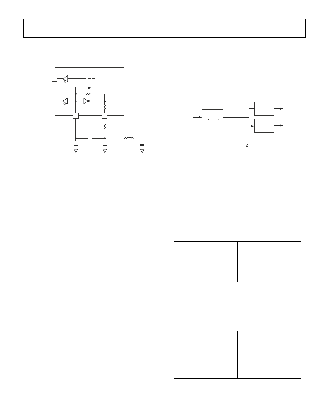
ADSP-BF522/ADSP-BF523/ADSP-BF524/ADSP-BF525/ADSP-BF526/ADSP-BF527
CLKIN
CLKOUT
XTAL
EN
CLKBUF
TO PLL CIRCUITRY
FOR OVERTONE
OPERATION ONLY:
NOTE: VALUES MARKED WITH * MUST BE CUSTOMIZED, DEPENDING
ON THE CRYSTAL AND LAYOUT. PLEASE ANALYZE CAREFULLY. FOR
FREQUENCIES ABOVE 33 MHz, THE SUGGE STED CAPACITOR VALUE
OF 18 pF SHOULD BE TREATED AS A MAXIMUM, AND THE SUGGESTED
RESISTOR VALUE SHOULD BE REDUCED TO 0 ⍀.
18 pF *
EN
18 pF *
330 ⍀*
BLACKFIN
560 ⍀
PLL
5u
to 64u
÷1to15
÷1,2,4,8
VCO
CLKIN
“FINE” ADJUSTMENT
REQUIRES PLL SEQUENCING
“COARSE” ADJUSTMENT
ON-THE-FLY
CCLK
SCLK
SCLK d CCLK
specified by the crystal manufacturer. The user should verify the
customized values based on careful investigations on multiple
devices over temperature range.
Figure 6. External Crystal Connections
A third-overtone crystal can be used for frequencies above 25
MHz. The circuit is then modified to ensure crystal operation
only at the third overtone by adding a tuned inductor circuit as
shown in Figure 6. A design procedure for third-overtone operation is discussed in detail in application note (EE-168) Using
Third Overtone Crystals with the ADSP-218x DSP on the Analog
Devices website (www.analog.com)—use site search on
“EE-168.”
The CLKBUF pin is an output pin, which is a buffered version
of the input clock. This pin is particularly useful in Ethernet
applications to limit the number of required clock sources in the
system. In this type of application, a single 25 MHz or 50 MHz
crystal may be applied directly to the processor. The 25 MHz or
50 MHz output of CLKBUF can then be connected to an external Ethernet MII or RMII PHY device. If, instead of a crystal, an
external oscillator is used at CLKIN, CLKBUF will not have the
40/60 duty cycle required by some devices. The CLKBUF output
is active by default and can be disabled for power savings reasons using the VR_CTL register.
The Blackfin core runs at a different clock rate than the on-chip
peripherals. As shown in Figure 7, the core clock (CCLK) and
system peripheral clock (SCLK) are derived from the input
clock (CLKIN) signal. An on-chip PLL is capable of multiplying
the CLKIN signal by a programmable multiplication factor
(bounded by specified minimum and maximum VCO frequencies). The default multiplier can be modified by a software
instruction sequence. This sequence is managed by the
bfrom_SysControl() function in the on-chip ROM.
On-the-fly CCLK and SCLK frequency changes can be applied
by using the bfrom_SysControl() function in the on-chip ROM.
The maximum allowed CCLK and SCLK rates depend on the
applied voltages V
, V
DDINT
DDEXT
, and V
DDMEM
; the VCO is always
Rev. C | Page 17 of 88 | March 2012
permitted to run up to the frequency specified by the part’s
maximum instruction rate. The CLKOUT pin reflects the SCLK
frequency to the off-chip world. It is part of the SDRAM interface, but it functions as a reference signal in other timing
specifications as well. While active by default, it can be disabled
using the EBIU_SDGCTL and EBIU_AMGCTL registers.
Figure 7. Frequency Modification Methods
All on-chip peripherals are clocked by the system clock (SCLK).
The system clock frequency is programmable by means of the
SSEL3–0 bits of the PLL_DIV register. The values programmed
into the SSEL fields define a divide ratio between the PLL output
(VCO) and the system clock. SCLK divider values are 1 through
15. Table 6 illustrates typical system clock ratios.
Note that the divisor ratio must be chosen to limit the system
clock frequency to its maximum of f
. The SSEL value can be
SCLK
dynamically changed without any PLL lock latencies by writing
the appropriate values to the PLL divisor register (PLL_DIV)
using the bfrom_SysControl() function in the on-chip ROM.
Table 6. Example System Clock Ratios
Example Frequency Ratios
Signal Name
SSEL3–0
Divider Ratio
VCO/SCLK
VCO SCLK
(MHz)
0001 1:1 100 100
0110 6:1 300 50
1010 10:1 500 50
The core clock (CCLK) frequency can also be dynamically
changed by means of the CSEL1–0 bits of the PLL_DIV register.
Supported CCLK divider ratios are 1, 2, 4, and 8, as shown in
Table 7. This programmable core clock capability is useful for
fast core frequency modifications.
Table 7. Core Clock Ratios
Example Frequency Ratios
Signal Name
CSEL1–0
Divider Ratio
VCO/CCLK
VCO CCLK
(MHz)
00 1:1 300 300
01 2:1 300 150
10 4:1 500 125
11 8:1 200 25

ADSP-BF522/ADSP-BF523/ADSP-BF524/ADSP-BF525/ADSP-BF526/ADSP-BF527
The maximum CCLK frequency not only depends on the part's
maximum instruction rate (see Page 87). This frequency also
depends on the applied V
voltage. See Table 12 and
DDINT
Table 15 for details. The maximal system clock rate (SCLK)
depends on the chip package and the applied V
and V
voltages (see Table 14 and Table 17).
DDMEM
DDINT
, V
DDEXT
,
BOOTING MODES
The processor has several mechanisms (listed in Table 8) for
automatically loading internal and external memory after a
reset. The boot mode is defined by four BMODE input pins
dedicated to this purpose. There are two categories of boot
modes. In master boot modes the processor actively loads data
from parallel or serial memories. In slave boot modes the processor receives data from external host devices.
The boot modes listed in Table 8 provide a number of mechanisms for automatically loading the processor’s internal and
external memories after a reset. By default, all boot modes use
the slowest meaningful configuration settings. Default settings
can be altered via the initialization code feature at boot time or
by proper OTP programming at pre-boot time. The BMODE
pins of the reset configuration register, sampled during poweron resets and software-initiated resets, implement the modes
shown in Table 8.
Table 8. Booting Modes
BMODE3–0 Description
0000 Idle — No boot
0001 Boot from 8- or 16-bit external flash memory
0010 Boot from 16-bit asynchronous FIFO
0011 Boot from serial SPI memory (EEPROM or flash)
0100 Boot from SPI host device
0101 Boot from serial TWI memory (EEPROM/flash)
0110 Boot from TWI host
0111 Boot from UART0 Host
1000 Boot from UART1 Host
1001 Reserved
1010 Boot from SDRAM
1011 Boot from OTP memory
1100 Boot from 8-bit NAND flash
via NFC using PORTF data pins
1101 Boot from 8-bit NAND flash
via NFC using PORTH data pins
1110 Boot from 16-Bit Host DMA
1111 Boot from 8-Bit Host DMA
• Idle/no boot mode (BMODE = 0x0) — In this mode, the
processor goes into idle. The idle boot mode helps recover
from illegal operating modes, such as when the OTP memory has been misconfigured.
• Boot from 8-bit or 16-bit external flash memory
(BMODE = 0x1) — In this mode, the boot kernel loads the
first block header from address 0x2000 0000, and (depending on instructions contained in the header) the boot
kernel performs an 8- or 16-bit boot or starts program execution at the address provided by the header. By default, all
configuration settings are set for the slowest device possible
(3-cycle hold time, 15-cycle R/W access times, 4-cycle
setup).
The ARDY is not enabled by default, but it can be enabled
through OTP programming. Similarly, all interface behavior and timings can be customized through OTP
programming. This includes activation of burst-mode or
page-mode operation. In this mode, all asynchronous
interface signals are enabled at the port muxing level.
• Boot from 16-bit asynchronous FIFO (BMODE = 0x2) —
In this mode, the boot kernel starts booting from address
0x2030 0000. Every 16-bit word that the boot kernel has to
read from the FIFO must be requested by placing a low
pulse on the DMAR1 pin.
• Boot from serial SPI memory, EEPROM or flash
(BMODE = 0x3) — 8-, 16-, 24-, or 32-bit addressable
devices are supported. The processor uses the PG1 GPIO
pin to select a single SPI EEPROM/flash device and submits a read command and successive address bytes (0x00)
until a valid 8-, 16-, 24-, or 32-bit addressable device is
detected. Pull-up resistors are required on the SPISEL1
and
MISO pins. By default, a value of 0x85 is written to the
SPI_BAUD register.
• Boot from SPI host device (BMODE = 0x4) — The processor operates in SPI slave mode and is configured to receive
the bytes of the LDR file from an SPI host (master) agent.
The HWAIT signal must be interrogated by the host before
every transmitted byte. A pull-up resistor is required on the
SPISS
input. A pull-down on the serial clock (SCK) may
improve signal quality and booting robustness.
• Boot from serial TWI memory, EEPROM/flash
(BMODE = 0x5) — The processor operates in master mode
and selects the TWI slave connected to the TWI with the
unique ID 0xA0.
The processor submits successive read commands to the
memory device starting at internal address 0x0000 and
begins clocking data into the processor. The TWI memory
device should comply with the Philips I
2C®
Bus Specification version 2.1 and should be able to auto-increment its
internal address counter such that the contents of the
memory device can be read sequentially. By default, a
PRESCALE value of 0xA and a TWI_CLKDIV value of
0x0811 are used. Unless altered by OTP settings, an I
2
C
memory that takes two address bytes is assumed. The
development tools ensure that data booted to memories
that cannot be accessed by the Blackfin core is written to an
intermediate storage location and then copied to the final
destination via memory DMA.
• Boot from TWI host (BMODE = 0x6) — The TWI host
selects the slave with the unique ID 0x5F.
The processor replies with an acknowledgement and the
host then downloads the boot stream. The TWI host agent
should comply with the Philips I
2
C Bus Specification
Rev. C | Page 18 of 88 | March 2012

ADSP-BF522/ADSP-BF523/ADSP-BF524/ADSP-BF525/ADSP-BF526/ADSP-BF527
version 2.1. An I2C multiplexer can be used to select one
processor at a time when booting multiple processors from
a single TWI.
• Boot from UART0 host on Port G (BMODE = 0x7) —
Using an autobaud handshake sequence, a boot-stream formatted program is downloaded by the host. The host
selects a bit rate within the UART clocking capabilities.
When performing the autobaud, the UART expects a “@”
(0x40) character (eight bits data, one start bit, one stop bit,
no parity bit) on the UART0RX pin to determine the bit
rate. The UART then replies with an acknowledgement
composed of 4 bytes (0xBF, the value of UART0_DLL, the
value of UART0_DLH, then 0x00). The host can then
download the boot stream. To hold off the host the Blackfin
processor signals the host with the boot host wait
(HWAIT) signal. Therefore, the host must monitor
HWAIT before every transmitted byte.
• Boot from UART1 host on Port F (BMODE = 0x8). Same
as BMODE = 0x7 except that the UART1 port is used.
• Boot from SDRAM (BMODE = 0xA) This is a warm boot
scenario, where the boot kernel starts booting from address
0x0000 0010. The SDRAM is expected to contain a valid
boot stream and the SDRAM controller must be configured
by the OTP settings.
• Boot from OTP memory (BMODE = 0xB) — This provides
a stand-alone booting method. The boot stream is loaded
from on-chip OTP memory. By default, the boot stream is
expected to start from OTP page 0x40 and can occupy all
public OTP memory up to page 0xDF. This is 2560 bytes.
Since the start page is programmable, the maximum size of
the boot stream can be extended to 3072 bytes.
• Boot from 8-bit external NAND flash memory (BMODE =
0xC and BMODE = 0xD) — In this mode, auto detection of
the NAND flash device is performed.
BMODE = 0xC, the processor configures PORTF GPIO
pins PF7:0 for the NAND data pins and PORTH pins
PH15:10 for the NAND control signals.
BMODE = 0xD, the processor configures PORTH GPIO
pins PH7:0 for the NAND data pins and PORTH pins
PH15:10 for the NAND control signals.
For correct device operation pull-up resistors are required
on both ND_CE
default, a value of 0x0033 is written to the NFC_CTL register. The booting procedure always starts by booting from
byte 0 of block 0 of the NAND flash device.
NAND flash boot supports the following features:
—Device Auto Detection
—Error Detection & Correction for maximum reliability
—No boot stream size limitation
—Peripheral DMA providing efficient transfer of all data
(excluding the ECC parity data)
(PH10) and ND_BUSY (PH13) signals. By
—Software-configurable boot mode for booting from
boot streams spanning multiple blocks, including bad
blocks
—Software-configurable boot mode for booting from
multiple copies of the boot stream, allowing for handling of bad blocks and uncorrectable errors
—Configurable timing via OTP memory
Small page NAND flash devices must have a 512-byte page
size, 32 pages per block, a 16-byte spare area size, and a bus
configuration of 8 bits. By default, all read requests from
the NAND flash are followed by four address cycles. If the
NAND flash device requires only three address cycles, the
device must be capable of ignoring the additional address
cycles.
The small page NAND flash device must comply with the
following command set:
—Reset: 0xFF
—Read lower half of page: 0x00
—Read upper half of page: 0x01
—Read spare area: 0x50
For large-page NAND-flash devices, the four-byte electronic signature is read in order to configure the kernel for
booting, which allows support for multiple large-page
devices. The fourth byte of the electronic signature must
comply with the specification in Table 9 on Page 20.
Any NAND flash array configuration from Table 9, excluding 16-bit devices, that also complies with the command set
listed below are directly supported by the boot kernel.
There are no restrictions on the page size or block size as
imposed by the small-page boot kernel.
For devices consisting of a five-byte signature, only four are
read. The fourth must comply as outlined above.
Large page devices must support the following command
set:
—Reset: 0xFF
—Read Electronic Signature: 0x90
—Read: 0x00, 0x30 (confirm command)
Large-page devices must not support or react to NAND
flash command 0x50. This is a small-page NAND flash
command used for device auto detection.
By default, the boot kernel will always issue five address
cycles; therefore, if a large page device requires only four
cycles, the device must be capable of ignoring the additional address cycles.
• Boot from 16-Bit Host DMA (BMODE = 0xE) — In this
mode, the host DMA port is configured in 16-bit Acknowledge mode, with little endian data formatting. Unlike other
modes, the host is responsible for interpreting the boot
stream. It writes data blocks individually into the Host
DMA port. Before configuring the DMA settings for each
block, the host may either poll the ALLOW_CONFIG bit in
HOST_STATUS or wait to be interrupted by the HWAIT
Rev. C | Page 19 of 88 | March 2012

ADSP-BF522/ADSP-BF523/ADSP-BF524/ADSP-BF525/ADSP-BF526/ADSP-BF527
signal. When using HWAIT, the host must still check
ALLOW_CONFIG at least once before beginning to configure the Host DMA Port. After completing the
configuration, the host is required to poll the READY bit in
HOST_STATUS before beginning to transfer data. When
the host sends an HIRQ control command, the boot kernel
issues a CALL instruction to address 0xFFA0 0000. It is the
host's responsibility to ensure that valid code has been
placed at this address. The routine at 0xFFA0 0000 can be a
simple initialization routine to configure internal
resources, such as the SDRAM controller, which then
returns using an RTS instruction. The routine may also by
the final application, which will never return to the boot
kernel.
• Boot from 8-Bit Host DMA (BMODE = 0xF) — In this
mode, the Host DMA port is configured in 8-bit interrupt
mode, with little endian data formatting. Unlike other
modes, the host is responsible for interpreting the boot
stream. It writes data blocks individually into the Host
DMA port. Before configuring the DMA settings for each
block, the host may either poll the ALLOW_CONFIG bit in
HOST_STATUS or wait to be interrupted by the HWAIT
signal. When using HWAIT, the host must still check
ALLOW_CONFIG at least once before beginning to configure the Host DMA Port. The host will receive an
interrupt from the HOST_ACK signal every time it is
allowed to send the next FIFO depths worth (sixteen 32-bit
words) of information. When the host sends an HIRQ control command, the boot kernel issues a CALL instruction to
address 0xFFA0 0000. It is the host's responsibility to
ensure valid code has been placed at this address. The routine at 0xFFA0 0000 can be a simple initialization routine
to configure internal resources, such as the SDRAM controller, which then returns using an RTS instruction. The
routine may also by the final application, which will never
return to the boot kernel.
Table 9. Fourth Byte for Large Page Devices
Bit Parameter Value Meaning
D1:D0 Page Size
(excluding spare area)
D2 Spare Area Size 00018 byte/512 byte
D5:D4 Block Size
(excluding spare area)
D6 Bus width 00
D3, D7 Not Used for configuration
00
01
10
11
16 byte/512 byte
00
01
10
11
01
1K byte
2K byte
4K byte
8K byte
64K byte
128K byte
256K byte
512K byte
x8
not supported
INSTRUCTION SET DESCRIPTION
The Blackfin processor family assembly language instruction set
employs an algebraic syntax designed for ease of coding and
readability. The instructions have been specifically tuned to provide a flexible, densely encoded instruction set that compiles to
a very small final memory size. The instruction set also provides
fully featured multifunction instructions that allow the programmer to use many of the processor core resources in a single
instruction. Coupled with many features more often seen on
microcontrollers, this instruction set is very efficient when compiling C and C++ source code. In addition, the architecture
supports both user (algorithm/application code) and supervisor (O/S kernel, device drivers, debuggers, ISRs) modes
of operation, allowing multiple levels of access to core
processor resources.
The assembly language, which takes advantage of the processor’s unique architecture, offers the following advantages:
• Seamlessly integrated DSP/MCU features are optimized for
both 8-bit and 16-bit operations.
• A multi-issue load/store modified-Harvard architecture,
which supports two 16-bit MAC or four 8-bit ALU + two
load/store + two pointer updates per cycle.
• All registers, I/O, and memory are mapped into a unified
4G byte memory space, providing a simplified programming model.
• Microcontroller features, such as arbitrary bit and bit-field
manipulation, insertion, and extraction; integer operations
on 8-, 16-, and 32-bit data-types; and separate user and
supervisor stack pointers.
• Code density enhancements, which include intermixing of
16-bit and 32-bit instructions (no mode switching, no code
segregation). Frequently used instructions are encoded
in 16 bits.
DEVELOPMENT TOOLS
The processor is supported with a complete set of
CROSSCORE® software and hardware development tools,
including Analog Devices emulators and VisualDSP++® development environment. The same emulator hardware that
supports other Blackfin processors also fully emulates the
ADSP-BF52x processors.
EZ-KIT Lite Evaluation Board
For evaluation of ADSP-BF52x processors, use the EZ-KIT Lite®
boards available from Analog Devices. Order using part numbers ADZS-BF526-EZLITE or ADZS-BF527-EZLITE. The
boards come with on-chip emulation capabilities and are
equipped to enable software development. Multiple daughter
cards are available.
DESIGNING AN EMULATOR-COMPATIBLE PROCESSOR BOARD (TARGET)
The Analog Devices family of emulators are tools that every system developer needs in order to test and debug hardware and
software systems. Analog Devices has supplied an IEEE 1149.1
Rev. C | Page 20 of 88 | March 2012

ADSP-BF522/ADSP-BF523/ADSP-BF524/ADSP-BF525/ADSP-BF526/ADSP-BF527
JTAG Test Access Port (TAP) on each JTAG processor. The
emulator uses the TAP to access the internal features of the processor, allowing the developer to load code, set breakpoints,
observe variables, observe memory, and examine registers. The
processor must be halted to send data and commands, but once
an operation has been completed by the emulator, the processor
system is set running at full speed with no impact on
system timing.
To use these emulators, the target board must include a header
that connects the processor’s JTAG port to the emulator.
For details on target board design issues including mechanical
layout, single processor connections, multiprocessor scan
chains, signal buffering, signal termination, and emulator pod
logic, see (EE-68) Analog Devices JTAG Emulation Technical
Reference on the Analog Devices website (www.analog.com)—
use site search on “EE-68.” This document is updated regularly
to keep pace with improvements to emulator support.
RELATED DOCUMENTS
The following publications that describe the ADSP-BF52x processors (and related processors) can be ordered from any
Analog Devices sales office or accessed electronically on
our website:
• Getting Started With Blackfin Processors
• ADSP-BF52x Blackfin Processor Hardware Reference (vol-
umes 1 and 2)
• Blackfin Processor Programming Reference
• ADSP-BF522/ADSP-BF524/ADSP-BF526 Blackfin Proces-
sor Anomaly List
• ADSP-BF523/ADSP-BF525/ADSP-BF527 Blackfin Processor Anomaly List
The Application Signal Chains page in the Circuits from the
TM
site (http:\\www.analog.com\signalchains) provides:
Lab
• Graphical circuit block diagram presentation of signal
chains for a variety of circuit types and applications
• Drill down links for components in each chain to selection
guides and application information
• Reference designs applying best practice design techniques
LOCKBOX SECURE TECHNOLOGY DISCLAIMER
Analog Devices products containing Lockbox Secure Technology are warranted by Analog Devices as detailed in the Analog
Devices Standard Terms and Conditions of Sale. To our knowledge, the Lockbox Secure Technology, when used in accordance
with the data sheet and hardware reference manual specifications, provides a secure method of implementing code and data
safeguards. However, Analog Devices does not guarantee that
this technology provides absolute security.
ACCORDINGLY, ANALOG DEVICES HEREBY DISCLAIMS
ANY AND ALL EXPRESS AND IMPLIED WARRANTIES
THAT THE LOCKBOX SECURE TECHNOLOGY CANNOT
BE BREACHED, COMPROMISED, OR OTHERWISE CIRCUMVENTED AND IN NO EVENT SHALL ANALOG
DEVICES BE LIABLE FOR ANY LOSS, DAMAGE,
DESTRUCTION, OR RELEASE OF DATA, INFORMATION,
PHYSICAL PROPERTY, OR INTELLECTUAL PROPERTY.
RELATED SIGNAL CHAINS
A signal chain is a series of signal-conditioning electronic components that receive input (data acquired from sampling either
real-time phenomena or from stored data) in tandem, with the
output of one portion of the chain supplying input to the next.
Signal chains are often used in signal processing applications to
gather and process data or to apply system controls based on
analysis of real-time phenomena. For more information about
this term and related topics, see the “signal chain” entry in
Wikipedia or the Glossary of EE Terms on the Analog Devices
website.
Analog Devices eases signal processing system development by
providing signal processing components that are designed to
work together well. A tool for viewing relationships between
specific applications and related components is available on the
www.analog.com website.
Rev. C | Page 21 of 88 | March 2012

ADSP-BF522/ADSP-BF523/ADSP-BF524/ADSP-BF525/ADSP-BF526/ADSP-BF527
SIGNAL DESCRIPTIONS
Signal definitions for the ADSP-BF52x processors are listed in
Table 10. In order to maintain maximum function and reduce
package size and ball count, some balls have dual, multiplexed
functions. In cases where ball function is reconfigurable, the
default state is shown in plain text, while the alternate function
is shown in italics.
All pins are three-stated during and immediately after reset,
with the exception of the external memory interface, asynchronous and synchronous memory control, and the buffered XTAL
output pin (CLKBUF). On the external memory interface, the
control and address lines are driven high, with the exception of
CLKOUT, which toggles at the system clock rate. During hibernate, all outputs are three-stated unless otherwise noted in
Table 10.
All I/O pins have their input buffers disabled with the exception
of the pins that need pull-ups or pull-downs, as noted in
Table 10.
It is strongly advised to use the available IBIS models to ensure
that a given board design meets overshoot/undershoot and signal integrity requirements. If no IBIS simulation is performed, it
is strongly recommended to add series resistor terminations for
all Driver Types A, C and D.
The termination resistors should be placed near the processor to
reduce transients and improve signal integrity. The resistance
value, typically 33 Ω or 47 Ω, should be chosen to match the
average board trace impedance.
Additionally, adding a parallel termination to CLKOUT may
prove useful in further enhancing signal integrity. Be sure to
verify overshoot/undershoot and signal integrity specifications
on actual hardware.
Table 10. Signal Descriptions
Signal Name Type Function
EBIU
ADDR19–1 O Address Bus A
DATA15–0 I/O Data Bus A
/SDQM1–0 O Byte Enables/Data Mask A
ABE1–0
AMS3–0 O Asynchronous Memory Bank Selects (Require pull-ups if hibernate is used.) A
ARDY I Hardware Ready Control
AOE
ARE
AWE O Asynchronous Write Enable A
SRAS
SCAS
SWE
SCKE O SDRAM Clock Enable (Requires a pull-down if hibernate with SDRAM self-
CLKOUT O SDRAM Clock Output B
SA10 O SDRAM A10 Signal A
SMS
O Asynchronous Output Enable A
O Asynchronous Read Enable A
O SDRAM Row Address Strobe A
O SDRAM Column Address Strobe A
OSDRAM Write Enable A
refresh is used.)
O SDRAM Bank Select A
Driver
Typ e
A
1
Rev. C | Page 22 of 88 | March 2012

ADSP-BF522/ADSP-BF523/ADSP-BF524/ADSP-BF525/ADSP-BF526/ADSP-BF527
Table 10. Signal Descriptions (Continued)
Driver
Signal Name Type Function
USB 2.0 HS OTG
USB_DP I/O Data + (This ball should be pulled low when USB is unused or not present.) F
USB_DM I/O Data – (This ball should be pulled low when USB is unused or not present.) F
USB_XI I USB Crystal Input (This ball should be pulled low when USB is unused or not
present.)
USB_XO O USB Crystal Output ( This ball should be left unconnected when USB is unused
or not present.)
USB_ID I USB OTG mode (This ball should be pulled low when USB is unused or not
present.)
USB_VREF A USB voltage reference (Connect to GND through a 0.1 μF capacitor or leave
unconnected when not used.)
USB_RSET A USB resistance set. (This ball should be left unconnected.)
USB_VBUS I/O 5V USB VBUS. USB_VBUS is an output only in peripheral mode during SRP
signaling. Host mode requires that an external voltage source of 5 V at 8 mA
or more (per the OTG specification) be applied to VBUS. The voltage source
needs to be able to charge and discharge VBUS, thus an ON/OFF switch is
required to control the voltage source. A GPIO can be used for this purpose
(This ball should be pulled low when USB is unused or not present.)
Port F: GPIO and Multiplexed Peripherals
PF0/PPI D0/DR0PRI /ND_D0A I/O GPIO/PPI Data 0/SPORT0 Primary Receive Data
/NAND Alternate Data 0
PF1/PPI D1/RFS0/ND_D1A I/O GPIO/PPI Data 1/SPORT0 Receive Frame Sync
/NAND Alternate Data 1
PF2/PPI D2/RSCLK0/ND_D2A I/O GPIO/PPI Data 2/SPORT0 Receive Serial Clock
/NAND Alternate Data 2/Alternate Capture Input 0
PF3/PPI D3/DT0PRI/ND_D3A I/O GPIO/PPI Data 3/SPORT0 Transmit Primary Data
/NAND Alternate Data 3
PF4/PPI D4/TFS0/ND_D4A/TACLK0 I/O GPIO/PPI Data 4/SPORT0 Transmit Frame Sync
/NAND Alternate Data 4/Alternate Timer Clock 0
PF5/PPI D5/TSCLK0/ND_D5A/
PF6/PPI D6/DT0SEC/ND_D6A/TACI 0 I/O GPIO/PPI Data 6/SPORT0 Transmit Secondary Data
PF7/PPI D7/DR0SEC/ND_D7A/TACI1 I/O GPIO/PPI Data 7/SPORT0 Receive Secondary Data
PF8/PPI D8/DR1PRI I/O GPIO/PPI Data 8/SPORT1 Primary Receive Data C
PF9/PPI D9/RSCLK1/SPISEL6
PF10/PPI D10/RFS1/SPISEL7
PF11/PPI D11/TFS1/CZM I/O GPIO/PPI Data 11/SPORT1 Transmit Frame Sync/Counter Zero Marker C
PF12/PPI D12/DT1PRI /SPISEL2
PF13/PPI D13/TSCLK1/SPISEL3
PF14/PPI D14/DT1SEC /UART1TX I/O GPIO/PPI Data 14/SPORT1 Transmit Secondary Data/UART1 Transmit C
PF15/PPI D15/DR1SEC/UART1RX/TAC I3 I/O GPIO/PPI Data 15/SPORT1 Receive Secondary Data
TAC LK 1 I/O GPIO/PPI Data 5/SPORT0 Transmit Serial Clock
/NAND Alternate Data 5/Alternate Timer Clock 1
/NAND Alternate Data 6/Alternate Capture Input 0
/NAND Alternate Data 7/Alternate Capture Input 1
I/O GPIO/PPI Data 9/SPORT1 Receive Serial Clock/SPI Slave Select 6 D
I/O GPIO/PPI Data 10/SPORT1 Receive Frame Sync/SPI Slave Select 7 C
/CDG I/O GPIO/PPI Data 12/SPORT1 Transmit Primary Data/SPI Slave Select 2/Counter
Down Gate
/CUD I/O GPIO/PPI Data 13/SPORT1 Transmit Serial Clock/SPI Slave Select 3/Counter Up
Direction
/UART1 Receive /Alternate Capture Input 3
Typ e
F
F
C
C
D
C
C
D
C
C
C
D
C
1
Rev. C | Page 23 of 88 | March 2012

ADSP-BF522/ADSP-BF523/ADSP-BF524/ADSP-BF525/ADSP-BF526/ADSP-BF527
Table 10. Signal Descriptions (Continued)
Driver
Signal Name Type Function
Port G: GPIO and Multiplexed Peripherals
PG0/HWAIT I/O GPIO/Boot Host Wait2 C
PG1/SPISS
PG2/SCK I/O GPIO/SPI Clock D
PG3/MISO/DR0SECA I/O GPIO/SPI Master In Slave Out/Sport 0 Alternate Receive Data Secondary C
PG4/MOSI/DT0SECA I/O GPIO/SPI Master Out Slave In/Sport 0 Alternate Transmit Data Secondary C
PG5/TMR1/PPI_FS2 I/O GPIO/Timer1/PPI Frame Sync2 C
PG6/DT0PR IA/TMR2/PPI_FS3 I/O GPIO/SPORT0 Alternate Primary Transmit Data / Timer2 / PPI Frame Sync3 C
PG7/TMR3/DR0PRIA/UART0T X I/O GPIO/Timer3/Sport 0 Alternate Receive Data Primary/UART0 Transmit C
PG8/TMR4/RFS0A/UART0RX/TAC I4 I/O GPIO/Timer 4/Sport 0 Alternate Receive Clock/Frame Sync
PG9/TMR5/RSCLK0A/TACI 5 I/O GPIO/Timer5/Sport 0 Alternate Receive Clock
PG10/TMR6/TSCLK0A/TAC I6 I/O GPIO/Timer 6
PG11/TMR7/HOST_WR
PG12/DMAR1/UART1TXA/HOST_ACK I/O GPIO/DMA Request 1/Alternate UART1 Transmit/Host DMA Acknowledge C
PG13/DMAR0/UART1RXA/HOST_ADDR/TAC I2 I/O GPIO/DMA Request 0/Alternate UART1 Receive/Host DMA Address/Alternate
PG14/TSCLK0A1/MDC/HOST_RD
PG15
Port H: GPIO and Multiplexed Peripherals
PH0/ND_D0/MIICRS/RMIICRSDV/HOST_D0 I/O GPIO/NAND D0/Ethernet MII or RMII Carrier Sense/Host DMA D0 C
PH1/ND_D1/ERxER/HOST_D1 I/O GPIO/NAND D1/Ethernet MII or RMII Receive Error/Host DMA D1 C
PH2/ND_D2/MDIO/HOST_D2 I/O GPIO/NAND D2/Ethernet Management Channel Serial Data/Host DMA D2 C
PH3/ND_D3/ETxEN/HOST_D3 I/O GPIO/NAND D3/Ethernet MII Transmit Enable/Host DMA D3 C
PH4/ND_D4/MIITxCLK/RMIIREF_CLK/HOST_D4 I/O GPIO/NAND D4/Ethernet MII or RMII Reference Clock/Host D4 C
PH5/ND_D5/ETxD0/HOST_D5 I/O GPIO/NAND D5/Ethernet MII or RMII Transmit D0/Host DMA D5 C
PH6/ND_D6/ERxD0/
PH7/ND_D7/ETxD1/HOST_D7 I/O GPIO/NAND D7/Ethernet MII or RMII Transmit D1/Host DMA D7 C
PH8/SPISEL4
PH9/SPISEL5
PH10/ND_CE
PH11/ND_WE/ETxD3/HOST_D11 I/O GPIO/NAND Write Enable/Ethernet MII Transmit D3/Host DMA D11 C
PH12/ND_RE
PH13/ND_BUSY/ERxCLK/HOST_D13 I/O GPIO/NAND Busy/Ethernet MII Receive Clock/Host DMA D13 C
PH14/ND_CLE/ERxDV/HOST_D14 I/O GPIO/NAND Command Latch Enable/Ethernet MII or RMII Receive Data Valid/
PH15/ND_ALE/COL/HOST_D15 I/O GPIO/NAND Address Latch Enable/Ethernet MII Collision/Host DMA Data 15 C
/SPISEL1 I/O GPIO/SPI Slave Select Input/SPI Slave Select 1 C
/UART0 Receive/Alternate Capture Input 4
/Alternate Capture Input 5
/Sport 0 Alternate Transmit
/Alternate Capture Input 6
I/O GPIO/Timer7/Host DMA Write Enable C
Capture Input 2
I/O GPIO/SPORT0 Alternate 1 Transmit/Ethernet Management Channel Clock
/Host DMA Read Enable
3
/TFS0A/MII PHYINT/RMII MDINT/HOST_CE I/O GPIO/SPORT0 Alternate Transmit Frame Sync/Ethernet/MII PHY Interrupt/RMII
Management Channel Data Interrupt/Host DMA Chip Enable
HOST_D6 I/O GPIO/NAND D6/Ethernet MII or RMII Receive D0/Host DMA D6 C
/ERxD1/HOST_D8/TACLK2 I/O GPIO/Alternate Timer Clock 2/Ethernet MII or RMII Receive D1/Host DMA D8
/SPI Slave Select 4
/ETxD2/HOST_D9/TACLK3 I/O GPIO/SPI Slave Select 5/Ethernet MII Transmit D2/Host DMA D9
/Alternate Timer Clock 3
/ERxD2/HOST_D10 I/O GPIO/NAND Chip Enable/Ethernet MII Receive D2/Host DMA D10 C
/ERxD3/HOST_D12 I/O GPIO/NAND Read Enable/Ethernet MII Receive D3/Host DMA D12 C
Host DMA D14
Typ e
C
D
D
C
D
C
C
C
C
1
Rev. C | Page 24 of 88 | March 2012

ADSP-BF522/ADSP-BF523/ADSP-BF524/ADSP-BF525/ADSP-BF526/ADSP-BF527
Table 10. Signal Descriptions (Continued)
Driver
Signal Name Type Function
Port J: Multiplexed Peripherals
PJ0 : PP I_F S1/ TMR0 I/O PPI Frame Sync1/Timer0 C
PJ1 : PP I_C LK/ TMRCLK I PPI Clock/Timer Clock
PJ2: SCL I/O 5V TWI Serial Clock (This pin is an open-drain output and requires a pull-up
PJ3: SDA I/O 5V TWI Serial Data (This pin is an open-drain output and requires a pull-up
resistor.
resistor.
4
)
4
)
Real Time Clock
RTXI I RTC Crystal Input (This ball should be pulled low when not used.)
RTXO O RTC Crystal Output (Does not three-state during hibernate.)
JTAG Port
TCK I JTAG Clock
TDO O JTAG Serial Data Out C
TDI I JTAG Serial Data In
TMS I JTAG Mode Select
TRST
EMU
I JTAG Reset (This ball should be pulled low if the JTAG port is not used.)
O Emulation Output C
Clock
CLKIN I Clock/Crystal Input
XTAL O Crystal Output (If CLKBUF is enabled, does not three-state during hibernate.)
CLKBUF O Buffered XTAL Output (If enabled, does not three-state during hibernate.) C
Mode Controls
RESET
I Reset
NMI I Nonmaskable Interrupt (This ball should be pulled high when not used.)
BMODE3–0 I Boot Mode Strap 3-0
ADSP-BF523/ADSP-BF525/ADSP-BF527 Voltage
Regulation I/F
VR
SEL
/EXT_WAKE1 O External FET Drive/Wake up Indication 1 (Does not three-state during
VR
OUT
I Internal/External Voltage Regulator Select
hibernate.)
EXT_WAKE0 O Wake up Indication 0 (Does not three-state during hibernate.) C
SS/PG
A Soft Start/Power Good
ADSP-BF522/ADSP-BF524/ADSP-BF526 Voltage
Regulation I/F
EXT_WAKE1 O Wake up Indication 1 (Does not three-state during hibernate.) C
EXT_WAKE0 O Wake up Indication 0 (Does not three-state during hibernate.) C
PG
A Power Good (This signal should be pulled low when not used.)
Typ e
E
E
G
1
Rev. C | Page 25 of 88 | March 2012

ADSP-BF522/ADSP-BF523/ADSP-BF524/ADSP-BF525/ADSP-BF526/ADSP-BF527
Table 10. Signal Descriptions (Continued)
Driver
Signal Name Type Function
Power Supplies ALL SUPPLIES MUST BE POWERED
See Operating Conditions for ADSP-BF523/ADSP-BF525/ADSP-BF527
Processors on Page 29, and see Operating Conditions for ADSP-BF522/
ADSP-BF524/ADSP-BF526 Processors on Page 27.
V
DDEXT
V
DDINT
V
DDRTC
V
DDUSB
V
DDMEM
V
DDOTP
V
PPOTP
PI/O Power Supply
P Internal Power Supply
P Real Time Clock Power Supply
P 3.3 V USB Phy Power Supply
PMEM Power Supply
POTP Power Supply
P OTP Programming Voltage
GND G Ground for All Supplies
1
See Output Drive Currents on Page 72 for more information about each driver type.
2
HWAIT must be pulled high or low to configure polarity. It is driven as an output and toggle during processor boot. See Booting Modes on Page 18.
3
When driven low, this ball can be used to wake up the processor from the hibernate state, either in normal GPIO mode or in Ethernet mode as MII PHYINT. If the ball is
used for wake up, enable the feature with the PHYWE bit in the VR_CTL register, and pull-up the ball with a resistor.
4
Consult version 2.1 of the I2C specification for the proper resistor value.
Typ e
1
Rev. C | Page 26 of 88 | March 2012

ADSP-BF522/ADSP-BF523/ADSP-BF524/ADSP-BF525/ADSP-BF526/ADSP-BF527
SPECIFICATIONS
Specifications are subject to change without notice.
OPERATING CONDITIONS FOR ADSP-BF522/ADSP-BF524/ADSP-BF526 PROCESSORS
Parameter Conditions Min Nominal Max Unit
V
DDINT
V
DDEXT
V
DDEXT
V
DDEXT
V
DDRTC
V
DDMEM
V
DDMEM
V
DDMEM
V
DDOTP
V
PPOTP
V
DDUSB
V
IH
V
IH
V
IH
8
V
IHTWI
V
IL
V
IL
V
IL
V
ILTWI
T
J
T
J
T
J
1
Must remain powered (even if the associated function is not used).
2
If not used, power with V
3
Balls that use V
to voltages higher than V
4
The V
PPOTP
on voltage and junction temperature) over the lifetime of the part. Please see Table 30 on Page 37 for details.
5
When not using the USB peripheral on the ADSP-BF524/ADSP-BF526 or terminating V
6
Bidirectional balls (PF15–0, PG15–0, PH15–0) and input balls (RTXI, TCK, TDI, TMS, TRST, CLKIN, RESET, NMI, and BMODE3–0) of the ADSP-BF52x processors are
3.3 V tolerant (always accept up to 3.6 V maximum VIH). Voltage compliance (on outputs, VOH) is limited by the V
7
Parameter value applies to all input and bidirectional balls, except USB_DP, USB_DM, USB_VBUS, SDA, and SCL.
8
The V
IHTWI
9
SDA and SCL are pulled up to V
Internal Supply Voltage 1.235 1.47 V
External Supply Voltage
External Supply Voltage
External Supply Voltage
RTC Power Supply Voltage
MEM Supply Voltage1,
MEM Supply Voltage1,
MEM Supply Voltage1,
OTP Supply Voltage
OTP Programming Voltage
1
1
1
2
3
3
3
1
1
1.7 1.8 1.9 V
2.25 2.5 2.75 V
33.33.6V
2.25 3.6 V
1.7 1.8 1.9 V
2.25 2.5 2.75 V
33.33.6V
2.25 2.5 2.75 V
For Reads 2.25 2.5 2.75 V
For Writes
USB Supply Voltage
High Level Input Voltage
High Level Input Voltage
High Level Input Voltage
High Level Input Voltage V
Low Level Input Voltage
Low Level Input Voltage
Low Level Input Voltage
Low Level Input Voltage V
Junction Temperature 289-Ball CSP_BGA
Junction Temperature 208-Ball CSP_BGA
Junction Temperature 208-Ball CSP_BGA
DDMEM
voltage for writes must only be applied when programming OTP memory. There is a finite amount of cumulative time that this voltage may be applied (dependent
min and max value vary with the selection in the TWI_DT field of the NONGPIO_DRIVE register. See V
4
5
6, 7
6, 7
6, 7
6, 7
6, 7
6, 7
V
DDEXT/VDDMEM
V
DDEXT/VDDMEM
V
DDEXT/VDDMEM
DDEXT
V
DDEXT/VDDMEM
V
DDEXT/VDDMEM
V
DDEXT/VDDMEM
DDEXT
= 1.90 V 1.1 V
= 2.75 V 1.7 V
= 3.6 V 2.0 V
= 1.90 V/2.75 V/3.6 V 0.7 × V
= 1.7 V 0.6 V
= 2.25 V 0.7 V
= 3.0 V 0.8 V
= Minimum 0.3 × V
6.9 7.0 7.1 V
3.0 3.3 3.6 V
BUSTWI
V
BUSTWI
BUSTWI
9
V
V
0+105°C
@T
=0°C to +70°C
AMBIENT
0+105°C
@T
=0°C to +70°C
AMBIENT
–40 +105 °C
@T
.
DDEXT
are DATA15–0, ADDR19–1, ABE1–0, ARE, AWE, AOE, AMS3–0, ARDY, SA10, SWE, SCAS, CLKOUT, SRAS, SMS, SCKE. These balls are not tolerant
DDMEM
.
BUSTWI
. See Table 11.
= –40°C to +85°C
AMBIENT
on the ADSP-BF522, V
DDUSB
must be powered by V
DDUSB
supply voltage.
DDEXT
min and max values in Table 11.
BUSTWI
DDEXT
.
Rev. C | Page 27 of 88 | March 2012

ADSP-BF522/ADSP-BF523/ADSP-BF524/ADSP-BF525/ADSP-BF526/ADSP-BF527
Table 11 shows settings for TWI_DT in the NONGPIO_DRIVE
register. Set this register prior to using the TWI port.
Table 11. TWI_DT Field Selections and V
TWI_DT V
000 (default)
1
Nominal V
DDEXT
3.3 2.97 3.3 3.63 V
DDEXT/VBUSTWI
Min V
BUSTWI
Nominal V
BUSTWI
Max Unit
BUSTWI
001 1.8 1.7 1.8 1.98 V
010 2.5 2.97 3.3 3.63 V
011 1.8 2.97 3.3 3.63 V
100 3.3 4.5 5 5.5 V
101 1.8 2.25 2.5 2.75 V
110 2.5 2.25 2.5 2.75 V
111 (reserved)–––––
1
Designs must comply with the V
DDEXT
and V
voltages specified for the default TWI_DT setting for correct JTAG boundary scan operation during reset.
BUSTWI
Clock Related Operating Conditions for ADSP-BF522/ADSP-BF524/ADSP-BF526 Processors
Table 12 describes the core clock timing requirements for the
ADSP-BF522/ADSP-BF524/ADSP-BF526 processors. Take care
in selecting MSEL, SSEL, and CSEL ratios so as not to exceed the
maximum core clock and system clock (see Table 14). Table 13
describes phase-locked loop operating conditions.
Table 12. Core Clock (CCLK) Requirements (All Instruction Rates1) for ADSP-BF522/ADSP-BF524/ADSP-BF526 Processors
Parameter Nominal Voltage Setting Max Unit
f
CCLK
f
CCLK
1
See the Ordering Guide on Page 87.
2
Applies to 400 MHz models only. See the Ordering Guide on Page 87.
Core Clock Frequency (V
Core Clock Frequency (V
=1.33 V minimum) 1.40 V 400
DDINT
= 1.235 V minimum) 1.30 V 300 MHz
DDINT
2
MHz
Table 13. Phase-Locked Loop Operating Conditions for ADSP-BF522/ADSP-BF524/ADSP-BF526 Processors
Parameter Min Max Unit
f
VCO
1
See the Ordering Guide on Page 87.
Voltage Controlled Oscillator (VCO) Frequency 70 Instruction Rate
1
MHz
Table 14. SCLK Conditions for ADSP-BF522/ADSP-BF524/ADSP-BF526 Processors
Parameter
f
SCLK
f
SCLK
1
If either V
2
f
must be less than or equal to f
SCLK
DDEXT
or V
DDMEM
CLKOUT/SCLK Frequency (V
CLKOUT/SCLK Frequency (V
are operating at 1.8V nominal, f
and is subject to additional restrictions for SDRAM interface operation. See Table 37 on Page 46.
CCLK
V
DDEXT/VDDMEM
1.8 V Nominal
1
V
DDEXT/VDDMEM
2.5 V or 3.3 V Nominal
Max Max Unit
≥ 1.33 V)
DDINT
< 1.33 V) 80 80 MHz
DDINT
is constrained to 80 MHz.
SCLK
2
80 100 MHz
Rev. C | Page 28 of 88 | March 2012

ADSP-BF522/ADSP-BF523/ADSP-BF524/ADSP-BF525/ADSP-BF526/ADSP-BF527
OPERATING CONDITIONS FOR ADSP-BF523/ADSP-BF525/ADSP-BF527 PROCESSORS
Parameter Conditions Min Nominal Max Unit
V
V
V
V
DDINT
DDINT
DDINT
DDEXT
Internal Supply Voltage
Internal Supply Voltage
Internal Supply Voltage
External Supply Voltage
1
Nonautomotive models
1
Automotive 533 MHz models
1
Automotive 400 MHz models31.045 1.10 1.20 V
4, 5
Nonautomotive models,
Internal Voltage Regulator
Disabled
V
DDEXT
V
DDEXT
V
DDEXT
V
DDRTC
V
DDRTC
V
DDMEM
V
DDMEM
V
DDMEM
V
DDMEM
V
DDOTP
V
PPOTP
V
DDUSB
V
IH
V
IH
V
IH
11
V
IHTWI
V
IL
V
IL
V
IL
V
ILTWI
T
J
T
J
T
J
T
J
1
The voltage regulator can generate V
specification is only guaranteed when the API is used.
2
See Ordering Guide on Page 87.
3
See Automotive Products on Page 86.
4
Must remain powered (even if the associated function is not used).
5
V
is the supply to the voltage regulator and GPIO.
DDEXT
6
If not used, power with V
7
Balls that use V
to voltages higher than V
8
When not using the USB peripheral on the ADSP-BF525/ADSP-BF527 or terminating V
9
Bidirectional balls (PF15–0, PG15–0, PH15–0) and input balls (RTXI, TCK, TDI, TMS, TRST, CLKIN, RESET, NMI, and BMODE3–0) of the ADSP-BF52x processors are
3.3 V tolerant (always accept up to 3.6 V maximum V
10
Parameter value applies to all input and bidirectional balls, except USB_DP, USB_DM, USB_VBUS, SDA, and SCL.
11
The V
IHTWI
12
SDA and SCL are pulled up to V
External Supply Voltage
External Supply Voltage
External Supply Voltage
RTC Power Supply Voltage
RTC Power Supply Voltage6Automotive models 2.7 3.3 3.6 V
MEM Supply Voltage
MEM Supply Voltage
MEM Supply Voltage
MEM Supply Voltage
OTP Supply Voltage
OTP Programming Voltage
USB Supply Voltage
High Level Input Voltage
High Level Input Voltage
High Level Input Voltage
High Level Input Voltage V
Low Level Input Voltage
Low Level Input Voltage
Low Level Input Voltage
Low Level Input Voltage V
Junction Temperature 289-Ball CSP_BGA
Junction Temperature 289-Ball CSP_BGA
Junction Temperature 208-Ball CSP_BGA
Junction Temperature 208-Ball CSP_BGA
DDINT
.
DDEXT
are DATA15–0, ADDR19–1, ABE1–0, ARE, AWE, AOE, AMS3–0, ARDY, SA10, SWE, SCAS, CLKOUT, SRAS, SMS, SCKE. These balls are not tolerant
DDMEM
min and max value vary with the selection in the TWI_DT field of the NONGPIO_DRIVE register. See V
DDMEM
.
BUSTWI
4, 5
Nonautomotive models 2.25 2.5 2.75 V
4, 5
Nonautomotive models 3 3.3 3.6 V
4, 5
Automotive models 2.7 3.3 3.6 V
6
Nonautomotive models 2.25 3.6 V
4, 7
4, 7
4, 7
4, 7
4
8
at levels of 1.00 V to 1.20 V with –5% to +5% tolerance when VRCTL is programmed with the bfrom_SysControl() API. This
. See Table 11 on Page 28.
Nonautomotive models 1.7 1.8 1.9 V
Nonautomotive models 2.25 2.5 2.75 V
Nonautomotive models 3 3.3 3.6 V
Automotive models 2.7 3.3 3.6 V
4
9, 10
V
DDEXT/VDDMEM
9, 10
V
DDEXT/VDDMEM
9, 10
V
DDEXT/VDDMEM
DDEXT
9, 10
V
DDEXT/VDDMEM
9, 10
V
DDEXT/VDDMEM
9, 10
V
DDEXT/VDDMEM
DDEXT
@T
AMBIENT
@T
AMBIENT
@T
AMBIENT
@T
AMBIENT
). Voltage compliance (on outputs, VOH) is limited by the V
IH
= 1.90 V 1.1 V
= 2.75 V 1.7 V
= 3.6 V 2.0 V
= 1.90 V/2.75 V/3.6 V 0.7 × V
= 1.7 V 0.6 V
= 2.25 V 0.7 V
= 3.0 V 0.8 V
= Minimum 0.3 × V
=0°C to +70°C
= –40°C to +70°C
=0°C to +70°C
= –40°C to +85°C
2
0.95 1.26 V
3
1.093 1.15 1.26 V
1.7 1.8 1.9 V
2.25 2.5 2.75 V
2.25 2.5 2.75 V
3.0 3.3 3.6 V
BUSTWI
V
BUSTWI
0 +105 °C
–40 +105 °C
0 +105 °C
–40 +105 °C
on the ADSP-BF523, V
DDUSB
must be powered by V
DDUSB
supply voltage.
DDEXT
min and max values in Table 11 on Page 28.
BUSTWI
DDEXT
BUSTWI
.
V
12
V
Rev. C | Page 29 of 88 | March 2012

ADSP-BF522/ADSP-BF523/ADSP-BF524/ADSP-BF525/ADSP-BF526/ADSP-BF527
Clock Related Operating Conditions for ADSP-BF523/ADSP-BF525/ADSP-BF527 Processors
Table 15 describes the core clock timing requirements for the
ADSP-BF523/ADSP-BF525/ADSP-BF527 processors. Take care
in selecting MSEL, SSEL, and CSEL ratios so as not to exceed the
maximum core clock and system clock (see Table 17). Table 16
describes phase-locked loop operating conditions.
Use the nominal voltage setting (Table 15) for internal and
external regulators.
Table 15. Core Clock (CCLK) Requirements (All Instruction Rates
1
) for ADSP-BF523/ADSP-BF525/ADSP-BF527 Processors
Parameter Nominal Voltage Setting Max Unit
f
CCLK
f
CCLK
f
CCLK
f
CCLK
1
See the Ordering Guide on Page 87.
2
Applies to 600 MHz models only. See the Ordering Guide on Page 87.
3
Applies to 533 MHz and 600 MHz models only. See the Ordering Guide on Page 87.
4
Applies only to automotive products. See Automotive Products on Page 86.
Core Clock Frequency (V
Core Clock Frequency (V
Core Clock Frequency (V
Core Clock Frequency (V
=1.14 V minimum) 1.20 V 600
DDINT
=1.093 V minimum) 1.15 V 533
DDINT
= 1.045 V minimum)
DDINT
= 0.95 V minimum) 1.0 V 400 MHz
DDINT
4
1.10 V 400 MHz
2
3
MHz
MHz
Table 16. Phase-Locked Loop Operating Conditions for ADSP-BF523/ADSP-BF525/ADSP-BF527 Processors
Parameter Min Max Unit
f
VCO
Voltage Controlled Oscillator (VCO) Frequency
60 Instruction Rate
1
MHz
(Commercial/Industrial Models)
f
VCO
Voltage Controlled Oscillator (VCO) Frequency
70 Instruction Rate
1
MHz
(Automotive Models)
1
See the Ordering Guide on Page 87.
Table 17. SCLK Conditions for ADSP-BF523/ADSP-BF525/ADSP-BF527 Processors
V
DDEXT/VDDMEM
1.8 V Nominal
1
V
DDEXT/VDDMEM
2.5 V or 3.3 V Nominal
Parameter Max Max Unit
f
SCLK
f
SCLK
1
If either V
2
f
3
Rounded number. Actual test specification is SCLK period of 7.5 ns. See Table 38 on Page 46.
DDEXT
must be less than or equal to f
SCLK
CLKOUT/SCLK Frequency (V
CLKOUT/SCLK Frequency (V
or V
are operating at 1.8V nominal, f
DDMEM
and is subject to additional restrictions for SDRAM interface operation. See Table 38 on Page 46.
CCLK
≥ 1.14 V)
DDINT
< 1.14 V)
DDINT
is constrained to 100 MHz.
SCLK
2
2
100 133
100 100 MHz
3
MHz
Rev. C | Page 30 of 88 | March 2012

ADSP-BF522/ADSP-BF523/ADSP-BF524/ADSP-BF525/ADSP-BF526/ADSP-BF527
ELECTRICAL CHARACTERISTICS
Table 18. Common Electrical Characteristics for All ADSP-BF52x Processors
Parameter Test Conditions Min Typical Max Unit
V
OH
V
OH
V
OH
V
OL
I
IH
I
IL
I
IHP
I
OZH
I
OZHTWI
I
OZL
C
IN
C
INTWI
1
Applies to input balls.
2
Applies to JTAG input balls (TCK, TDI, TMS, TRST).
3
Applies to three-statable balls.
4
Applies to bidirectional balls SCL and SDA.
5
Applies to all signal balls, except SCL and SDA.
6
Guaranteed, but not tested.
High Level Output Voltage V
High Level Output Voltage V
High Level Output Voltage V
Low Level Output Voltage V
High Level Input Current
Low Level Input Current
1
1
High Le vel Input Current JTAG
Three-State Leakage Current
Three-State Leakage Current
Three-State Leakage Current3V
Input Capacitance
Input Capacitance
5,6
4,6
DDEXT/VDDMEM
=–0.5mA
I
OH
DDEXT/VDDMEM
= 1.7 V,
= 2.25 V,
IOH=–0.5mA
DDEXT/VDDMEM
= 3.0 V,
IOH=–0.5mA
DDEXT/VDDMEM
= 1.7/2.25/3.0 V,
IOL=2.0mA
V
DDEXT/VDDMEM
=3.6 V,
VIN=3.6V
V
DDEXT/VDDMEM
2
V
DDEXT
3
V
DDEXT/VDDMEM
=3.6V
V
IN
4
V
DDEXT
DDEXT/VDDMEM
fIN = 1 MHZ, T
=2.5V
V
IN
fIN = 1 MHZ, T
=3.6 V, VIN = 0 V 10.0 μA
= 3.6 V, VIN = 3.6 V 75.0 μA
= 3.6 V,
=3.0 V, VIN = 5.5 V 10.0 μA
= 3.6 V, VIN = 0 V 10.0 μA
= 25°C,
AMBIENT
= 25°C,
AMBIENT
VIN=2.5V
1.35 V
2.0 V
2.4 V
0.4 V
10.0 μA
10.0 μA
58pF
15 pF
Rev. C | Page 31 of 88 | March 2012

ADSP-BF522/ADSP-BF523/ADSP-BF524/ADSP-BF525/ADSP-BF526/ADSP-BF527
Table 19. Electrical Characteristics for ADSP-BF522/ADSP-BF524/ADSP-BF526 Processors
Parameter Test Conditions Min Typical Max Unit
I
DDDEEPSLEEP
I
DDSLEEP
1
V
Current in
DDINT
Deep Sleep Mode
V
Current in
DDINT
V
= 1.3 V, f
DDINT
= 25°C, ASF = 0.00
T
J
V
= 1.3 V, f
DDINT
= 0 MHz, f
CCLK
= 25 MHz, T
SCLK
=0MHz,
SCLK
= 25°C 13 mA
J
Sleep Mode
I
DD-IDLE
I
DD-TYP
I
DD-TYP
I
DDHIBERNATE
I
DDRTC
I
DDUSB-FS
Current in
DDINT
Idle
V
Current V
DDINT
V
Current V
DDINT
1,
2Hibernate State
Current
V
Current V
DDRTC
V
Current in
DDUSB
V
= 1.3 V, f
DDINT
= 25°C, ASF = 0.4
T
J
= 1.3 V, f
DDINT
T
= 25°C, ASF = 1.00
J
= 1.4 V, f
DDINT
T
= 25°C, ASF = 1.00
J
V
DDEXT=VDDMEM=VDDRTC=VDDUSB
V
DDOTP=VPPOTP
with voltage regulator off (V
= 3.3 V, TJ = 25°C 20 μA
DDRTC
V
= 3.3 V, TJ = 25°C, Full Speed USB Transmit 9 mA
DDUSB
= 300 MHz, f
CCLK
= 300 MHz, f
CCLK
= 400 MHz, f
CCLK
= 25 MHz,
SCLK
= 25 MHz,
SCLK
= 25 MHz,
SCLK
=3.30V,
=2.5 V, TJ= 25°C, CLKIN = 0 MHz
= 0 V)
DDINT
V
Full/Low Speed
Mode
I
DDUSB-HS
V
DDUSB
Current in
V
= 3.3 V, TJ = 25°C, High Speed USB Transmit 25 mA
DDUSB
High Speed Mode
1, 3
I
DDSLEEP
V
DDINIT
Current in
f
= 0 MHz, f
CCLK
> 0 MHz Tab le 22 +
SCLK
Sleep Mode
I
DDDEEPSLEEP
1, 3
V
DDINT
Current in
f
= 0 MHz, f
CCLK
= 0 MHz Tab le 22 mA
SCLK
Deep Sleep Mode
I
DDINT
I
DDOTP
I
DDOTP
I
PPOTP
I
PPOTP
3, 5
V
Current f
DDINT
V
Current V
DDOTP
V
Current V
DDOTP
V
Current V
PPOTP
V
Current V
PPOTP
> 0 MHz, f
CCLK
= 2.5 V, TJ = 25°C, OTP Memory Read 2 mA
DDOTP
= 2.5 V, TJ = 25°C, OTP Memory Write 2 mA
DDOTP
= 2.5 V, TJ = 25°C, OTP Memory Read 100 μA
PPOTP
= see Tab le 30 , TJ=25°C, OTPMemory
PPOTP
≥ 0 MHz Tab le 22 +
SCLK
Write
1
See the ADSP-BF52x Blackfin Processor Hardware Reference Manual for definition of sleep, deep sleep, and hibernate operating modes.
2
Includes current on V
3
Guaranteed maximum specifications.
4
Unit for V
5
See Table 21 for the list of I
is V (Volts). Unit for f
DDINT
, V
DDEXT
DDUSB
power vectors covered.
DDINT
, V
, V
DDOTP
, and V
DDMEM
is MHz. Example: 1.4 V, 75 MHz would be 0.52 × 1.4 × 75 MHz = 54.6 mA adder.
SCLK
supplies. Clock inputs are tied high or low.
PPOTP
2mA
44 mA
83 mA
114 mA
40 μA
mA
4
× f
(0.52 × V
DDINT
SCLK
)
mA
(Tab le 23 × ASF) +
× f
(0.52 × V
DDINT
SCLK
)
3mA
4
Rev. C | Page 32 of 88 | March 2012

ADSP-BF522/ADSP-BF523/ADSP-BF524/ADSP-BF525/ADSP-BF526/ADSP-BF527
Table 20. Electrical Characteristics for ADSP-BF523/ADSP-BF525/ADSP-BF527 Processors
Parameter Test Conditions Min Typical Max Unit
I
DDDEEPSLEEP
I
DDSLEEP
1
V
Current in
DDINT
Deep Sleep Mode
V
Current in
DDINT
V
= 1.0 V, f
DDINT
= 25°C, ASF = 0.00
T
J
V
= 1.0 V, f
DDINT
= 0 MHz, f
CCLK
= 25 MHz, TJ = 25°C 20 mA
SCLK
=0MHz,
SCLK
Sleep Mode
I
DD-IDLE
I
DD-TYP
Current in
DDINT
Idle
V
Current V
DDINT
V
= 1.0 V, f
DDINT
= 25°C, ASF = 0.44
T
J
= 1.0 V, f
DDINT
= 400 MHz, f
CCLK
= 400 MHz, f
CCLK
= 25 MHz,
SCLK
= 25 MHz,
SCLK
V
TJ = 25°C, ASF = 1.00
I
DD-TYP
Current V
DDINT
DDINT
= 1.15 V, f
= 533 MHz, f
CCLK
= 25 MHz,
SCLK
V
TJ = 25°C, ASF = 1.00
I
DD-TYP
I
DDHIBERNATE
I
DDRTC
I
DDUSB-FS
DDINT
1, 2
Hibernate State
Current
V
DDRTC
V
DDUSB
Current V
Current V
Current in
= 1.2 V, f
DDINT
T
= 25°C, ASF = 1.00
J
V
DDEXT=VDDMEM=VDDRTC
V
DDOTP=VPPOTP
with voltage regulator off (V
= 3.3 V, TJ = 25°C 20 μA
DDRTC
V
= 3.3 V, TJ = 25°C, Full Speed USB Transmit 9 mA
DDUSB
= 600 MHz, f
CCLK
= V
DDUSB
= 25 MHz,
SCLK
=3.30V,
=2.5 V, TJ= 25°C, CLKIN = 0 MHz
= 0 V)
DDINT
V
Full/Low Speed
Mode
I
DDUSB-HS
I
DDSLEEP
1, 3
Current in
DDUSB
High Speed Mode
V
Current in
DDINT
V
= 3.3 V, TJ = 25°C, High Speed USB
DDUSB
Transmit
f
= 0 MHz, f
CCLK
> 0 MHz Tab le 2 4 + (0.61 ×
SCLK
V
Sleep Mode
I
DDDEEPSLEEP
1, 3
V
DDINT
Current in
f
CCLK
= 0 MHz, f
= 0 MHz Tab le 2 4 mA
SCLK
Deep Sleep Mode
3, 5
I
DDINT
I
DDOTP
I
DDOTP
I
PPOTP
I
PPOTP
1
See the ADSP-BF52x Blackfin Processor Hardware Reference Manual for definition of sleep, deep sleep, and hibernate operating modes.
2
Includes current on V
3
Guaranteed maximum specifications.
4
Unit for V
5
See Table 21 for the list of I
V
Current f
DDINT
V
Current V
DDOTP
V
Current V
DDOTP
V
Current V
PPOTP
V
Current V
PPOTP
DDEXT
is V (Volts). Unit for f
DDINT
CCLK
DDOTP
DDOTP
PPOTP
PPOTP
, V
, V
DDUSB
DDMEM
is MHz. Example: 1.2 V, 75 MHz would be 0.61 x 1.2 x 75 = 54.9 mA adder.
SCLK
power vectors covered.
DDINT
> 0 MHz, f
≥ 0 MHz Tab le 2 4 + (Ta bl e 2 5
SCLK
= 2.5 V, TJ = 25°C, OTP Memory Read 1 mA
= 2.5 V, TJ = 25°C, OTP Memory Write 25 mA
= 2.5 V, TJ = 25°C, OTP Memory Read 0 mA
= 2.5 V, TJ= 25°C, OTP Memory Write 0 mA
, V
DDOTP
, and V
supplies. Clock inputs are tied high or low.
PPOTP
10 mA
53 mA
94 mA
144 mA
170 mA
40 μA
25 mA
mA
V
DDINT
× f
SCLK
4
)
mA
× ASF) + (0.61 × V
)
× f
SCLK
DDINT
4
Rev. C | Page 33 of 88 | March 2012

ADSP-BF522/ADSP-BF523/ADSP-BF524/ADSP-BF525/ADSP-BF526/ADSP-BF527
Total Power Dissipation
Total power dissipation has two components:
1. Static, including leakage current
2. Dynamic, due to transistor switching characteristics
Many operating conditions can also affect power dissipation,
including temperature, voltage, operating frequency, and processor activity. Electrical Characteristics on Page 31 shows the
current dissipation for internal circuitry (V
DDINT
). I
DDDEEPSLEEP
specifies static power dissipation as a function of voltage
) and temperature (see Table 22 or Table 24), and I
(V
DDINT
DDINT
specifies the total power specification for the listed test conditions, including the dynamic component as a function of voltage
(V
) and frequency (Table 23 or Table 25).
DDINT
There are two parts to the dynamic component. The first part is
due to transistor switching in the core clock (CCLK) domain.
This part is subject to an Activity Scaling Factor (ASF) which
represents application code running on the processor core and
L1 memories (Table 21).
The ASF is combined with the CCLK Frequency and V
DDINT
dependent data in Table 23 or Table 25 to calculate this part.
The second part is due to transistor switching in the system
clock (SCLK) domain, which is included in the I
DDINT
specifica-
tion equation.
Table 21. Activity Scaling Factors (ASF)
I
Power Vector Activity Scaling Factor (ASF)
DDINT
I
DD-PEAK
I
DD-HIGH
I
DD-TYP
I
DD-APP
I
DD-NOP
I
DD-IDLE
1
See Estimating Power for ASDP-BF534/BF536/BF537 Blackfin Processors
(EE-297). The power vector information also applies to the ADSP-BF52x
processors.
1.29
1.26
1.00
0.88
0.72
0.44
1
Table 22. Static Current — I
1
TJ (°C)
1.2 V 1.25 V 1.3 V 1.35 V 1.4 V 1.45 V 1.5 V
DD-DEEPSLEEP
(mA) for ADSP-BF522/ADSP-BF524/ADSP-BF526 Processors
Voltage (V
DDINT
1
)
–40 1.47 1.42 1.50 1.64 1.85 2.12 2.09
–20 1.67 1.81 1.89 1.95 2.01 2.07 2.12
0 1.97 2.07 2.15 2.22 2.30 2.39 2.47
25 2.49 2.66 2.79 2.92 3.07 3.20 3.36
40 3.12 3.37 3.57 3.75 3.96 4.18 4.40
55 4.07 4.47 4.82 5.11 5.41 5.73 6.06
70 5.77 6.28 6.71 7.17 7.61 8.09 8.60
85 8.32 8.88 9.56 10.25 10.94 11.63 12.36
100 12.11 12.93 13.94 14.76 15.76 16.77 17.83
105 13.78 14.72 15.74 16.81 17.91 19.06 20.27
1
Valid temperature and voltage ranges are model-specific. See Operating Conditions for ADSP-BF522/ADSP-BF524/ADSP-BF526 Processors on Page 27.
Table 23. Dynamic Current in CCLK Domain (mA, with ASF = 1.0)1 for ADSP-BF522/ADSP-BF524/ADSP-BF526 Processors
f
CCLK
(MHz)
2
1.2 V 1.25 V 1.3 V 1.35 V 1.4 V 1.45 V 1.5 V
Voltage (V
DDINT
2
)
400 N/A N/A 91.41 95.7 100.11 104.51 109.01
350 N/A N/A 80.56 84.37 88.26 92.17 96.17
300 63.31 66.51 69.78 73.09 76.51 79.93 83.42
250 53.36 56.10 58.88 61.72 64.64 67.56 70.55
200 43.49 45.76 48.08 50.44 52.86 55.28 57.77
100 23.6 24.93 26.29 27.68 29.12 30.56 32.04
1
The values are not guaranteed as standalone maximum specifications. They must be combined with static current per the equations of Electrical Characteristics on Page 31.
2
Valid frequency and voltage ranges are model-specific. See Operating Conditions for ADSP-BF522/ADSP-BF524/ADSP-BF526 Processors on Page 27.
Rev. C | Page 34 of 88 | March 2012

ADSP-BF522/ADSP-BF523/ADSP-BF524/ADSP-BF525/ADSP-BF526/ADSP-BF527
Table 24. Static Current — I
1
TJ (°C)
0.95 V 1.00 V 1.05 V 1.10 V 1.15 V 1.20 V 1.25 V 1.30 V
DD-DEEPSLEEP
(mA) for ADSP-BF523/ADSP-BF525/ADSP-BF527 Processors
Voltage (V
DDINT
1
)
–40 6.5 7.8 9.3 11.1 13.1 15.4 18.0 21.0
–20 9.0 10.6 12.4 14.6 17.0 19.8 22.9 26.4
0 13.2 15.2 17.7 20.4 23.5 27.0 30.9 35.3
25 22.3 25.4 28.9 32.8 37.2 42.1 47.6 53.7
40 30.8 34.8 39.2 44.1 49.6 55.7 62.5 70.0
55 42.9 47.9 53.6 59.9 66.9 74.6 83.2 92.6
70 59.1 65.6 72.9 80.8 89.7 99.4 110.2 122.0
85 80.4 88.6 97.9 107.8 119.2 131.5 145.1 159.8
100 109.3 118.7 130.5 143.2 157.4 172.8 189.7 208.1
105 120.8 132.1 144.7 158.8 174.2 190.9 209.3 229.2
115 144.4 157.5 172.3 188.4 206.0 225.3 246.4 269.2
125 173.9 189.1 206.4 224.9 245.4 267.8 292.2 318.7
1
Valid temperature and voltage ranges are model-specific. See Operating Conditions for ADSP-BF523/ADSP-BF525/ADSP-BF527 Processors on Page 29.
Table 25. Dynamic Current in CCLK Domain (mA, with ASF = 1.0)1 for ADSP-BF523/ADSP-BF525/ADSP-BF527 Processors
f
CCLK
(MHz)
2
0.95 V 1.00 V 1.05 V 1.10 V 1.15 V 1.20 V 1.25 V 1.30 V
Voltage (V
DDINT
2
)
600 N/A N/A N/A N/A 130.4 137.6 145.1 152.5
533 N/A N/A N/A 110.3 116.7 123.3 129.8 136.4
500 N/A N/A 97.3 103.1 109.1 115.0 121.3 127.7
400 69.8 74.3 78.9 83.6 88.5 93.5 98.6 103.9
300 53.4 56.9 60.4 64.1 68.0 71.8 75.8 80.0
200 36.9 39.4 41.9 44.6 47.4 50.1 53.0 56.0
100 20.5 22.0 23.6 25.3 27.0 28.8 30.6 32.5
1
The values are not guaranteed as standalone maximum specifications. They must be combined with static current per the equations of Electrical Characteristics on Page 31.
2
Valid frequency and voltage ranges are model-specific. See Operating Conditions for ADSP-BF523/ADSP-BF525/ADSP-BF527 Processors on Page 29.
Rev. C | Page 35 of 88 | March 2012

ADSP-BF522/ADSP-BF523/ADSP-BF524/ADSP-BF525/ADSP-BF526/ADSP-BF527
ABSOLUTE MAXIMUM RATINGS
Stresses greater than those listed in Table 26 may cause permanent damage to the device. These are stress ratings only.
Functional operation of the device at these or any other condi-
tions greater than those indicated in the operational sections of
this specification is not implied. Exposure to absolute maximum
rating conditions for extended periods may affect device
reliability.
Table 26. Absolute Maximum Ratings
Parameter Rating
Internal Supply Voltage (V
Internal Supply Voltage (V
External (I/O) Supply Voltage (V
Real-Time Clock Supply Voltage (V
OTP Supply Voltage (V
OTP Programming Voltage (V
OTP Programming Voltage (V
USB PHY Supply Voltage (V
Input Voltage
Input Voltage3, 4,
Input Voltage
3, 4, 5
6
3, 4, 7
Output Voltage Swing –0.5 V to V
Current per Pin Group3,
I
OH/IOL
) for ADSP-BF523/ADSP-BF525/ADSP-BF527 processors –0.3 V to +1.26 V
DDINT
) for ADSP-BF522/ADSP-BF524/ADSP-BF526 processors –0.3 V to +1.47 V
DDINT
DDEXT/VDDMEM
DDRTC
) –0.5 V to +3.0 V
DDOTP
)1 –0.5 V to +3.0 V
PPOTP
2
)
PPOTP
) –0.5 V to +3.8 V
DDUSB
) –0.3 V to +3.8 V
) –0.5 V to +3.8 V
–0.5 V to +7.1 V
–0.5 V to +3.8 V
–0.5 V to +5.5 V
–0.5 V to +5.25 V
8
82 mA (max)
DDEXT/VDDMEM
+0.5 V
Storage Temperature Range –65°C to +150°C
Junction Temperature While Biased +110°C
1
Applies to OTP memory reads and writes for ADSP-BF523/ADSP-BF525/ADSP-BF527 processors and to OTP memory reads for ADSP-BF522/ADSP-BF524/ADSP-BF526
processors.
2
Applies only to OTP memory writes for ADSP-BF522/ADSP-BF524/ADSP-BF526 processors.
3
Applies to 100% transient duty cycle.
4
Applies only when V
5
For other duty cycles see Table 27.
6
Applies to balls SCL and SDA.
7
Applies to balls USB_DP, USB_DM, and USB_VBUS.
8
For pin group information, see Table 28. For other duty cycles see Table 29.
is within specifications. When V
DDEXT
is outside specifications, the range is V
DDEXT
DDEXT
±0.2 V.
Table 27. Maximum Duty Cycle for Input Transient Volt-
1, 2
age
Maximum Duty Cycle3VIN Min (V)
4
VIN Max (V)
6
100% –0.50 +3.80
40% –0.70 +4.00
25% –0.80 +4.10
15% –0.90 +4.20
10% –1.00 +4.30
1
Applies to all signal balls with the exception of CLKIN, XTAL, VR
EXT_WAKE1, SCL, SDA, USB_DP, USB_DM, and USB_VBUS.
2
Applies only when V
cations, the range is V
3
Duty cycle refers to the percentage of time the signal exceeds the value for the 100%
case. The is equivalent to the measured duration of a single instance of overshoot
or undershoot as a percentage of the period of occurrence.
4
The individual values cannot be combined for analysis of a single instance of
overshoot or undershoot. The worst case observed value must fall within one of the
voltages specified, and the total duration of the overshoot or undershoot (exceeding
the 100% case) must be less than or equal to the corresponding duty cycle.
is within specifications. When V
DDEXT
±0.2 V.
DDEXT
DDEXT
/
OUT
is outside specifi-
Rev. C | Page 36 of 88 | March 2012
Table 26 specifies the maximum total source/sink (I
OH/IOL
) current for a group of pins. Permanent damage can occur if this
value is exceeded. To understand this specification, if pins PH4,
PH3, PH2, PH1, and PH0 from group 1 in Table 28 were sourcing or sinking 2 mA each, the total current for those pins would
be 10 mA. This would allow up to 72 mA total that could be
sourced or sunk by the remaining pins in the group without
damaging the device. For a list of all groups and their pins, see
the Table 28 table. For duty cycles that are less than 100%, see
Table 29. Note that the V
and VOL specifications have separate
OH
per-pin maximum current requirements (see Table 19 on
Page 32 and Table 20 on Page 33).
Table 28. Total Current Pin Groups
Group Pins in Group
1 PH4, PH3, PH2, PH1, PH0, PF15, PF14, PF13
2 PF12, SDA, SCL, PF11, PF10, PF9, PF8, PF7
3 PF6, PF5, PF4, PF3, PF2, PF1, PF0, PPI_FS1
4 PPI_CLK, PG15, PG14, PG13, PG12, PG11, PG10, PG9
5 PG8, PG7, PG6, PG5, PG4, BMODE3, BMODE2, BMODE1

ADSP-BF522/ADSP-BF523/ADSP-BF524/ADSP-BF525/ADSP-BF526/ADSP-BF527
vvvvvv .x n. n
tppZccc
ADSP-BF52x
a
#yyww country_of_origin
B
ESD
(electrostatic discharge) sensitive device.
Charged devices and circuit boards can discharge
without detection. Although this product features
patented or proprietary protection circuitry, damage
may occur on devices subjected to high energy ESD.
Therefore, proper ESD precautions should be taken to
avoid
performance degradation or loss of functionality.
Table 28. Total Current Pin Groups (Continued)
Group Pins in Group
6 BMODE0, PG3, PG2, PG1, PG0, TDI, TDO, EMU
7TCK, TRST
, TMS
8 PH12, PH11, PH10, PH9, PH8, PH7, PH6, PH5
9 PH15, PH14, PH13, CLKBUF, NMI
, RESET
10 DATA 15, D ATA14, DATA13, DATA1 2, DATA 11, DATA 1 0
11 DATA 9, DATA8, DATA7, DATA 6 , DATA5, DATA 4
12 DATA3, DATA2, DATA1, DATA0, ADDR19, ADDR18
13 ADDR17, ADDR16, ADDR15, ADDR14, ADDR13
14 ADDR12, ADDR11, ADDR10, ADDR9, ADDR8, ADDR7
15 ADDR6, ADDR5, ADDR4, ADDR3, ADDR2, ADDR1
16 ABE1
, ABE0, SA10, SWE, SCAS, SRAS
17 SMS, SCKE, ARDY, AWE, ARE, AOE
18 AMS3, AMS2, AMS1, AMS0, CLKOUT
Table 29. Maximum Duty Cycle for IOH/IOL Current Per Pin
Group
Maximum Duty Cycle RMS Current (mA)
100% 82
80% 92
60% 106
40% 130
25% 165
10% 261
When programming OTP memory on the ADSP-BF522/
ADSP-BF524/ADSP-BF526 processors, the VPPOTP ball must
be set to the write value specified in the Operating Conditions
for ADSP-BF522/ADSP-BF524/ADSP-BF526 Processors on
Page 27. There is a finite amount of cumulative time that the
write voltage may be applied (dependent on voltage and junction temperature) to VPPOTP over the lifetime of the part.
Therefore, maximum OTP memory programming time for the
ADSP-BF522/ADSP-BF524/ADSP-BF526 processors is shown
in Table 30. The ADSP-BF523/ADSP-BF525/ADSP-BF527 processors do not have a similar restriction.
PACKAGE INFORMATION
The information presented in Figure 8 and Table 31 provides
details about the package branding for the ADSP-BF52x processors. For a complete listing of product availability, see Ordering
Guide on Page 87.
Figure 8. Product Information on Package
Table 31. Package Brand Information
1
Brand Key Field Description
ADSP-BF52x Product Name
2
t Temperature Range
pp Package Type
Z Lead Free Option
ccc See Ordering Guide
vvvvvv.x Assembly Lot Code
n.n Silicon Revision
# RoHS Compliance Designator
yyww Date Code
1
Non Automotive only. For branding information specific to Automotive
products, contact Analog Devices Inc.
2
See product names in the Ordering Guide on Page 87.
ESD SENSITIVITY
Table 30. Maximum OTP Memory Programming Time for
ADSP-BF522/ADSP-BF524/ADSP-BF526 Processors
V
PPOTP
6.9 6000 sec 100 sec 25 sec
7.0 2400 sec 44 sec 12 sec
7.1 1000 sec 18 sec 4.5 sec
Temperature (TJ)
Voltage (V) 25°C 85°C 105°C
Rev. C | Page 37 of 88 | March 2012

ADSP-BF522/ADSP-BF523/ADSP-BF524/ADSP-BF525/ADSP-BF526/ADSP-BF527
CLKIN
t
WRST
t
CKIN
t
CKINL
t
CKINH
t
BUFDLAY
t
BUFDLAY
RESET
CLKBUF
TIMING SPECIFICATIONS
Specifications are subject to change without notice.
Clock and Reset Timing
Table 32 and Figure 9 describe clock and reset operations. Per
the CCLK and SCLK timing specifications in Table 12 to
Table 17, combinations of CLKIN and clock multipliers must
not select core/peripheral clocks in excess of the processor's
maximum instruction rate.
Table 32. Clock and Reset Timing
Parameter MinMaxUnit
Timing Requirements
f
CKIN
t
CKINL
t
CKINH
t
WRST
CLKIN Frequency (Commercial/ Industrial Models)
CLKIN Frequency (Automotive Models)
CLKIN Low Pulse
CLKIN High Pulse
1
1
RESET Asserted Pulse Width Low
1, 2, 3, 4
5
Switching Characteristic
t
BUFDLAY
1
Applies to PLL bypass mode and PLL nonbypass mode.
2
Combinations of the CLKIN frequency and the PLL clock multiplier must not exceed the allowed f
Table 14 on Page 28 and Table 15 on Page 30 through Table 17 on Page 30.
3
The t
period (see Figure 9) equals 1/f
CKIN
4
If the DF bit in the PLL_CTL register is set, the minimum f
5
Applies after power-up sequence is complete. See Table 33 and Figure 10 for power-up reset timing.
CLKIN to CLKBUF Delay 10 ns
.
CKIN
specification is 24 MHz for commercial/industrial models and 28 MHz for automotive models.
CKIN
1, 2, 3, 4
12 50 MHz
14 50 MHz
10 ns
10 ns
11 × t
CKIN
, f
, and f
VCO
CCLK
settings discussed in Table 12 on Page 28 through
SCLK
ns
Figure 9. Clock and Reset Timing
Rev. C |Page 38 of 88 | March 2012

ADSP-BF522/ADSP-BF523/ADSP-BF524/ADSP-BF525/ADSP-BF526/ADSP-BF527
RESET
t
RST_IN_PWR
CLKIN
V
DD_SUPPLIES
Table 33. Power-Up Reset Timing
Parameter MinMaxUnit
Timing Requirements
t
RST_IN_PWR
RESET Deasserted after the V
DDINT
, V
DDEXT
Pins are Stable and Within Specification
In Figure 10, V
DD_SUPPLIES
, V
, V
, V
, V
DDMEM
DDEXT
, V
, V
DDOTP
DDRTC
DDRTC
is V
DDUSB
DDINT
Figure 10. Power-Up Reset Timing
, and CLKIN
, V
, V
DDUSB
DDMEM
3500 × t
, and V
CKIN
DDOTP
ns
.
Rev. C |Page 39 of 88 | March 2012

ADSP-BF522/ADSP-BF523/ADSP-BF524/ADSP-BF525/ADSP-BF526/ADSP-BF527
t
HARDY
SETUP
2 CYCLES
PROGRAMMED READ
ACCESS 4 CYCLES
ACCESS EXTENDED
3 CYCLES
HOLD
1 CYCLE
t
DO
t
HO
t
DO
t
HARDY
t
SARDY
t
SDAT
t
HDAT
t
SARDY
CLKOUT
AMSx
ABE1–0
ADDR19–1
AOE
ARE
ARDY
DATA 15–0
t
HO
Asynchronous Memory Read Cycle Timing
Table 34. Asynchronous Memory Read Cycle Timing
Parameter
MinMaxMinMaxMinMaxMinMaxUnit
Timing Requirements
t
SDAT
t
HDAT
t
SARDY
t
HARDY
DATA15– 0 Setup Before CLKOUT 2.12.12.12.1 ns
DATA15– 0 Hold After CLKOUT 1.20.80.90.8 ns
ARDY Setup Before CLKOUT 4.04.04.04.0 ns
ARDY Hold After CLKOUT 0.20.20.20.2 ns
Switching Characteristics
t
DO
t
HO
1
Output balls include AMS3– 0, ABE1–0, ADDR19–1, AOE, ARE.
Output Delay After CLKOUT
Output Hold After CLKOUT
1
1
0.80.80.80.8 ns
ADSP-BF522/ADSP-BF524/
ADSP-BF526
V
DDMEM
1.8 V Nominal
2.5 V or 3.3 V
V
DDMEM
Nominal
ADSP-BF523/ADSP-BF525/
ADSP-BF527
V
DDMEM
1.8 V Nominal
2.5 V or 3.3 V
Nominal
6.06.06.06.0 ns
V
DDMEM
Figure 11. Asynchronous Memory Read Cycle Timing
Rev. C |Page 40 of 88 | March 2012

ADSP-BF522/ADSP-BF523/ADSP-BF524/ADSP-BF525/ADSP-BF526/ADSP-BF527
SETUP
2 CYCLES
PROGRAMMED
WRITE
ACCESS
2 CYCLES
ACCESS
EXTEND
1 CYCLE
HOLD
1 CYCLE
t
DO
t
HO
CLKOUT
AMSx
ABE1–0
ADDR19–1
AWE
ARDY
DATA 15–0
t
SARDY
t
SARDY
t
DDAT
t
ENDAT
t
HARDY
t
HO
t
DO
t
HARDY
Asynchronous Memory Write Cycle Timing
Table 35. Asynchronous Memory Write Cycle Timing
ADSP-BF522/ADSP-BF524/
V
DDMEM
1.8 V Nominal
Parameter
MinMaxMinMaxMinMaxMinMaxUnit
Timing Requirements
t
SARDY
t
HARDY
ARDY Setup Before CLKOUT 4.04.04.04.0 ns
ARDY Hold After CLKOUT 0.20.20.20.2 ns
Switching Characteristics
t
DDAT
t
ENDAT
t
DO
t
HO
1
Output balls include AMS3– 0, ABE1–0, ADDR19–1, DATA15– 0, AWE.
DATA15 – 0 Disable After CLKOUT 6.06.06.06.0 ns
DATA15 – 0 Enable After CLKOUT 0.00.00.00.0 ns
Output Delay After CLKOUT
Output Hold After CLKOUT
1
1
0.80.80.80.8 ns
ADSP-BF523/ADSP-BF525/
ADSP-BF526
2.5 V or 3.3 V
V
DDMEM
Nominal
1.8 V Nominal
V
DDMEM
ADSP-BF527
2.5 V or 3.3 V
V
DDMEM
Nominal
6.06.06.06.0 ns
Figure 12. Asynchronous Memory Write Cycle Timing
Rev. C |Page 41 of 88 | March 2012

ADSP-BF522/ADSP-BF523/ADSP-BF524/ADSP-BF525/ADSP-BF526/ADSP-BF527
NAND Flash Controller Interface Timing
Table 36 and Figure 13 on Page 43 through Figure 17 on
Page 45 describe NAND Flash Controller Interface operations.
Table 36. NAND Flash Controller Interface Timing
V
DDEXT
1.8 V Nominal
2.5 V or 3.3 V Nominal
V
DDEXT
Parameter MinMinUnit
Write Cycle
Switching Characteristics
t
CWL
t
CH
t
CLEWL
t
CLH
t
ALEWL
t
ALH
t
WP
t
WHWL
t
WC
t
DWS
t
DWH
ND_CE Setup Time to AWE Low 1.0 × t
ND_CE Hold Time From AWE High 3.0 × t
ND_CLE Setup Time to AWE Low 0.00.0 ns
ND_CLE Hold Time From AWE high 2.5 × t
ND_ALE Setup Time to AWE Low 0.00.0 ns
ND_ALE Hold Time From AWE High 2.5 × t
1
AWE Low to AWE high (WR_DLY +1.0) × t
AWE High to AWE Low 4.0 × t
1
1
AWE Low to AWE Low (WR_DLY +5.0) × t
Data Setup Time for a Write Access (WR_DLY +1.5) × t
Data Hold Time for a Write Access 2.5 × t
– 4 1.0 × t
SCLK
– 4 3.0 × t
SCLK
– 4 2.5 × t
SCLK
– 4 2.5 × t
SCLK
– 4 (WR_DLY +1.0) × t
SCLK
– 4 4.0 × t
SCLK
– 4 (WR_DLY +5.0) × t
SCLK
– 4 (WR_DLY +1.5) × t
SCLK
– 4 2.5 × t
SCLK
– 4 ns
SCLK
– 4 ns
SCLK
– 4 ns
SCLK
– 4 ns
SCLK
– 4 ns
SCLK
– 4 ns
SCLK
– 4 ns
SCLK
– 4 ns
SCLK
– 4 ns
SCLK
Read Cycle
Switching Characteristics
t
CRL
t
CRH
t
RP
t
RHRL
t
RC
ND_CE Setup Time to ARE Low 1.0 × t
ND_CE Hold Time From ARE High 3.0 × t
1
ARE Low to ARE High (RD_DLY +1 .0) × t
ARE High to ARE Low 4.0 × t
1
ARE Low to ARE Low (RD_DLY +5.0) × t
– 4 1.0 × t
SCLK
– 4 3.0 × t
SCLK
– 4 (RD_DLY +1.0) × t
SCLK
– 4 4.0 × t
SCLK
– 4 (RD_DLY +5.0) × t
SCLK
– 4 ns
SCLK
– 4 ns
SCLK
– 4 ns
SCLK
– 4 ns
SCLK
– 4 ns
SCLK
Timing Requirements (ADSP-BF522/ADSP-BF524/ADSP-BF526)
t
t
DRS
DRH
Data Setup Time for a Read Transaction 14.010.0 ns
Data Hold Time for a Read Transaction 0.00.0 ns
Timing Requirements (ADSP-BF523/ADSP-BF525/ADSP-BF527)
t
t
DRS
DRH
Data Setup Time for a Read Transaction 11.08.0 ns
Data Hold Time for a Read Transaction 0.00.0 ns
Write Followed by Read
Switching Characteristics
t
WHRL
1
WR_DLY and RD_DLY are defined in the NFC_CTL register.
AWE High to ARE Low 5.0 × t
– 4 5.0 × t
SCLK
– 4 ns
SCLK
Rev. C |Page 42 of 88 | March 2012

ADSP-BF522/ADSP-BF523/ADSP-BF524/ADSP-BF525/ADSP-BF526/ADSP-BF527
t
CLEWL
t
ALEWL
ND_DATA
t
CH
t
CWL
t
CLH
t
ALH
t
DWH
ND_CE
ND_CLE
ND_ALE
AWE
t
WP
t
DWS
ND_DATA
t
WP
t
WP
t
ALH
t
ALH
ND_CE
ND_CLE
ND_ALE
AWE
t
CWL
t
CLEWL
t
ALEWL
t
WHWL
t
WC
t
DWS
t
DWH
t
DWS
t
DWH
t
ALEWL
In Figure 13, ND_DATA is ND_D0–D7.
Figure 13. NAND Flash Controller Interface Timing — Command Write Cycle
In Figure 14, ND_DATA is ND_D0–D7.
Figure 14. NAND Flash Controller Interface Timing — Address Write Cycle
Rev. C |Page 43 of 88 | March 2012

ADSP-BF522/ADSP-BF523/ADSP-BF524/ADSP-BF525/ADSP-BF526/ADSP-BF527
ND_DATA
ND_CE
ND_CLE
ND_ALE
AWE
t
CWL
t
CLEWL
t
ALEWL
t
WC
t
DWS
t
DWH
t
DWS
t
DWH
t
WHWL
t
WP
t
WP
ND_DATA
t
RP
ND_CLE
ND_CE
ND_ALE
ARE
t
CRL
t
CRH
t
RP
t
RHRL
t
RC
t
DRS
t
DRH
t
DRS
t
DRH
In Figure 15, ND_DATA is ND_D0–D7.
Figure 15. NAND Flash Controller Interface Timing — Data Write Operation
In Figure 16, ND_DATA is ND_D0–D7.
Figure 16. NAND Flash Controller Interface Timing — Data Read Operation
Rev. C |Page 44 of 88 | March 2012

ADSP-BF522/ADSP-BF523/ADSP-BF524/ADSP-BF525/ADSP-BF526/ADSP-BF527
ND_DATA
ND_CLE
t
CLWL
t
CLEWL
t
CLH
ARE
AWE
t
DWS
t
DWH
t
DRS
t
DRH
t
WHRL
t
WP
t
RP
ND_CE
In Figure 17, ND_DATA is ND_D0–D7.
Figure 17. NAND Flash Controller Interface Timing — Write Followed by Read Operation
Rev. C |Page 45 of 88 | March 2012

ADSP-BF522/ADSP-BF523/ADSP-BF524/ADSP-BF525/ADSP-BF526/ADSP-BF527
SDRAM Interface Timing
Table 37. SDRAM Interface Timing for ADSP-BF522/ADSP-BF524/ADSP-BF526 Processors
V
DDMEM
1.8V Nominal
Parameter
MinMaxMinMaxUnit
Timing Requirements
t
SSDAT
t
HSDAT
Data Setup Before CLKOUT 1.51.5 ns
Data Hold After CLKOUT 1.30.8 ns
Switching Characteristics
t
SCLK
t
SCLKH
t
SCLKL
t
DCAD
t
HCAD
t
DSDAT
t
ENSDAT
1
The t
value is the inverse of the f
SCLK
2
Command balls include: SRAS, SCAS, SWE, SDQM, SMS, SA10, SCKE.
CLKOUT Period
CLKOUT Width High 5.04.0 ns
CLKOUT Width Low 5.04.0 ns
Command, Address, Data Delay After CLKOUT
Command, Address, Data Hold After CLKOUT
Data Disable After CLKOUT 5.55.0 ns
Data Enable After CLKOUT 0.00.0 ns
1
2
2
specification discussed in Table 14 and Table 17. Package type and reduced supply voltages affect the best-case values listed here.
SCLK
12.510 ns
5.04.0 ns
1.01.0 ns
Table 38. SDRAM Interface Timing for ADSP-BF523/ADSP-BF525/ADSP-BF527 Processors
V
DDMEM
1.8V Nominal
Parameter
MinMaxMinMaxUnit
Timing Requirements
t
SSDAT
t
HSDAT
Data Setup Before CLKOUT 1.51.5 ns
Data Hold After CLKOUT 1.00.8 ns
Switching Characteristics
t
SCLK
t
SCLKH
t
SCLKL
t
DCAD
t
HCAD
t
DSDAT
t
ENSDAT
1
The t
value is the inverse of the f
SCLK
2
Command balls include: SRAS, SCAS, SWE, SDQM, SMS, SA10, SCKE.
CLKOUT Period
CLKOUT Width High 2.52.5 ns
CLKOUT Width Low 2.52.5 ns
Command, Address, Data Delay After CLKOUT
Command, Address, Data Hold After CLKOUT
Data Disable After CLKOUT 5.04.0 ns
Data Enable After CLKOUT 0.00.0 ns
1
2
2
specification discussed in Table 14 and Table 17. Package type and reduced supply voltages affect the best-case values listed here.
SCLK
10 7.5 ns
4.04.0 ns
1.01.0 ns
V
DDMEM
2.5 V or 3.3V Nominal
V
DDMEM
2.5 V or 3.3V Nominal
Rev. C |Page 46 of 88 | March 2012

ADSP-BF522/ADSP-BF523/ADSP-BF524/ADSP-BF525/ADSP-BF526/ADSP-BF527
t
SCLK
CLKOUT
t
SCLKL
t
SCLKH
t
SSDAT
t
HSDAT
t
ENSDAT
t
DCAD
t
DSDAT
t
HCAD
t
DCAD
t
HCAD
DATA (IN)
DATA (OUT)
COMMAND,
ADDRESS
(OUT)
NOTE: COMMAND = SRAS, SCAS, SWE, SDQM, SMS, SA10, SCKE.
Figure 18. SDRAM Interface Timing
Rev. C |Page 47 of 88 | March 2012

ADSP-BF522/ADSP-BF523/ADSP-BF524/ADSP-BF525/ADSP-BF526/ADSP-BF527
CLKOUT
t
DS
DMAR0/1
(ACTIVE LOW)
DMAR0/1
(ACTIVE HIGH)
t
DMARACT
t
DMARINACT
t
DH
External DMA Request Timing
Table 40 and Figure 19 describe the External DMA Request
operations.
Table 39. External DMA Request Timing for ADSP-BF522/ADSP-BF524/ADSP-BF526 Processors
V
DDEXT/VDDMEM
1.8 V Nominal
Parameter
MinMaxMinMaxUnit
Timing Requirements
t
DS
t
DH
t
DMARACT
t
DMARINACT
1
Because the external DMA control pins are part of the V
V
are NOT equal may require level shifting logic for correct operation.
DDMEM
DMARx Asserted to CLKOUT High Setup 9.06.0 ns
CLKOUT High to DMARx Deasserted Hold Time 0.00.0 ns
DMARx Active Pulse Width 1.0 × t
DMARx Inactive Pulse Width 1.75 × t
power domain and the CLKOUT signal is part of the V
DDEXT
SCLK
SCLK
power domain, systems in which V
DDMEM
Table 40. External DMA Request Timing for ADSP-BF523/ADSP-BF525/ADSP-BF527 Processors
V
DDEXT/VDDMEM
1.8 V Nominal
Parameter
MinMaxMinMaxUnit
Timing Requirements
t
DS
t
DH
t
DMARACT
t
DMARINACT
1
Because the external DMA control pins are part of the V
V
are NOT equal may require level shifting logic for correct operation.
DDMEM
DMARx Asserted to CLKOUT High Setup 8.06.0 ns
CLKOUT High to DMARx Deasserted Hold Time 0.00.0 ns
DMARx Active Pulse Width 1.0 × t
DMARx Inactive Pulse Width 1.75 × t
power domain and the CLKOUT signal is part of the V
DDEXT
SCLK
SCLK
power domain, systems in which V
DDMEM
1
V
DDEXT/VDDMEM
2.5 V or 3.3 V Nominal
1.0 × t
SCLK
1.75 × t
SCLK
1
V
DDEXT/VDDMEM
2.5 V or 3.3 V Nominal
1.0 × t
SCLK
1.75 × t
SCLK
DDEXT
DDEXT
ns
ns
and
ns
ns
and
Figure 19. External DMA Request Timing
Rev. C |Page 48 of 88 | March 2012

ADSP-BF522/ADSP-BF523/ADSP-BF524/ADSP-BF525/ADSP-BF526/ADSP-BF527
Parallel Peripheral Interface Timing
Table 41 and Figure 20 on Page 50, Figure 24 on Page 54, and
Figure 27 on Page 56 describe parallel peripheral interface
operations.
Table 41. Parallel Peripheral Interface Timing for ADSP-BF522/ADSP-BF524/ADSP-BF526 Processors
V
Parameter
DDEXT
1.8V Nominal
MinMaxMinMaxUnit
2.5 V or 3.3 V Nominal
Timing Requirements
t
PCLKW
t
PCLK
PPI_CLK Width
PPI_CLK Period
1
1
6.46.4 ns
25.020.0 ns
Timing Requirements - GP Input and Frame Capture Modes
t
SFSPE
External Frame Sync Setup Before PPI_CLK
6.76.7 ns
(Nonsampling Edge for Rx, Sampling Edge for Tx)
t
HFSPE
t
SDRPE
t
HDRPE
External Frame Sync Hold After PPI_CLK 1.21.2 ns
Receive Data Setup Before PPI_CLK 4.13.5 ns
Receive Data Hold After PPI_CLK 2.01.6 ns
Switching Characteristics - GP Output and Frame Capture Modes
t
DFSPE
t
HOFSPE
t
DDTPE
t
HDTPE
1
PPI_CLK frequency cannot exceed f
Internal Frame Sync Delay After PPI_CLK 8.08.0 ns
Internal Frame Sync Hold After PPI_CLK 1.71.7 ns
Transmit Data Delay After PPI_CLK 8.28.0 ns
Transmit Data Hold After PPI_CLK 2.31.9 ns
/2
SCLK
Table 42. Parallel Peripheral Interface Timing for ADSP-BF523/ADSP-BF525/ADSP-BF527 Processors
V
Parameter
DDEXT
1.8V Nominal
MinMaxMinMaxUnit
2.5 V or 3.3V Nominal
Timing Requirements
t
PCLKW
t
PCLK
PPI_CLK Width
PPI_CLK Period
1
1
6.06.0 ns
20.015.0 ns
Timing Requirements - GP Input and Frame Capture Modes
t
SFSPE
External Frame Sync Setup Before PPI_CLK
6.76.7 ns
(Nonsampling Edge for Rx, Sampling Edge for Tx)
t
HFSPE
t
SDRPE
t
HDRPE
External Frame Sync Hold After PPI_CLK 1.01.0 ns
Receive Data Setup Before PPI_CLK 3.53.5 ns
Receive Data Hold After PPI_CLK 2.01.6 ns
Switching Characteristics - GP Output and Frame Capture Modes
t
DFSPE
t
HOFSPE
t
DDTPE
t
HDTPE
1
PPI_CLK frequency cannot exceed f
Internal Frame Sync Delay After PPI_CLK 8.08.0 ns
Internal Frame Sync Hold After PPI_CLK 1.71.7 ns
Transmit Data Delay After PPI_CLK 8.08.0 ns
Transmit Data Hold After PPI_CLK 2.31.9 ns
/2
SCLK
V
V
DDEXT
DDEXT
Rev. C |Page 49 of 88 | March 2012

ADSP-BF522/ADSP-BF523/ADSP-BF524/ADSP-BF525/ADSP-BF526/ADSP-BF527
t
PCLK
t
SFSPE
DATA SAMPLED /
FRAME SYNC SAMPLED
DATA SAMPLED /
FRAME SYNC SAMPLED
PPI_DATA
PPI_CLK
PPI_FS1/2
t
HFSPE
t
HDRPE
t
SDRPE
t
PCLKW
t
HDTPE
t
SFSPE
DATA DRIVEN /
FRAME SYNC SAMPLED
PPI_DATA
PPI_CLK
PPI_FS1/2
t
HFSPE
t
DDTPE
t
PCLK
t
PCLKW
t
HDRPE
t
SDRPE
t
HOFSPE
FRAME SYNC
DRIVEN
DATA
SAMPLED
PPI_DATA
PPI_CLK
PPI_FS1/2
t
DFSPE
t
PCLK
t
PCLKW
Figure 20. PPI GP Rx Mode with External Frame Sync Timing
Figure 21. PPI GP Tx Mode with External Frame Sync Timing
Figure 22. PPI GP Rx Mode with Internal Frame Sync Timing
Rev. C |Page 50 of 88 | March 2012

ADSP-BF522/ADSP-BF523/ADSP-BF524/ADSP-BF525/ADSP-BF526/ADSP-BF527
t
HOFSPE
FRAME SYNC
DRIVEN
DATA
DRIVEN
PPI_DATA
PPI_CLK
PPI_FS1/2
t
DFSPE
t
DDTPE
t
HDTPE
t
PCLK
t
PCLKW
DATA
DRIVEN
Figure 23. PPI GP Tx Mode with Internal Frame Sync Timing
Rev. C |Page 51 of 88 | March 2012

ADSP-BF522/ADSP-BF523/ADSP-BF524/ADSP-BF525/ADSP-BF526/ADSP-BF527
Serial Ports
Table 43 through Table 47 on Page 56 and Figure 24 on Page 54
through Figure 27 on Page 56 describe serial port operations.
Table 43. Serial Ports—External Clock
ADSP-BF522/ADSP-BF524/ADSP-BF526 ADSP-BF523/ADSP-BF525/
ADSP-BF527
V
V
DDEXT
1.8V Nominal
Parameter
V
DDEXT
1.8V Nominal
2.5 V or 3 .3V Nominal
V
DDEXT
MinMaxMinMaxMinMaxMinMaxUnit
Timing Requirements
t
TFSx/RFSx Setup Before TSCLKx
SFSE
t
HFSE
t
SDRE
t
HDRE
t
SCLKEW
t
SCLKE
t
SUDTE
t
SUDRE
1
RSCLKx
TFSx/RFSx Hold After TSCLKx/RSCLKx13.03.03.03.0 ns
Receive Data Setup Before RSCLKx13.03.03.03.0 ns
Receive Data Hold After RSCLKx
TSCLKx/RSCLKx Width 7.04.57.04.5 ns
TSCLKx/RSCLKx Period 2.0 × t
Start-Up Delay From SPORT Enable To
First External TFSx
Start-Up Delay From SPORT Enable To
First External RFSx
2
2
3.03.03.03.0 ns
1
3.53.03.53.0 ns
4.0 × t
4.0 × t
SCLK
SCLKE
SCLKE
2.0 × t
4.0 × t
4.0 × t
SCLK
SCLKE
SCLKE
2.0 × t
4.0 × t
4.0 × t
SCLK
SCLKE
SCLKE
2.0 × t
4.0 × t
4.0 × t
Switching Characteristics
TFSx/RFSx Delay After TSCLKx/RSCLKx
t
DFSE
(Internally Generated TFSx/RFSx)
TFSx/RFSx Hold After TSCLKx/RSCLKx
t
HOFSE
(Internally Generated TFSx/RFSx)
t
Transmit Data Delay After TSCLKx
DDTE
Transmit Data Hold After TSCLKx
t
HDTE
1
Referenced to sample edge.
2
Verified in design but untested.
3
Referenced to drive edge.
3
0.00.00.00.0 ns
3
3
3
0.00.00.00.0 ns
10.010.010.010.0 ns
10.010.010.010.0 ns
DDEXT
2.5 V or 3.3V
Nominal
SCLK
SCLKE
SCLKE
ns
ns
ns
Rev. C |Page 52 of 88 | March 2012

ADSP-BF522/ADSP-BF523/ADSP-BF524/ADSP-BF525/ADSP-BF526/ADSP-BF527
Table 44. Serial Ports—Internal Clock for ADSP-BF522/ADSP-BF524/ADSP-BF526 Processors
V
DDEXT
1.8V Nominal
Parameter
MinMaxMinMaxUnit
Timing Requirements
t
t
t
t
TFSx/RFSx Setup Before TSCLKx/RSCLKx
SFSI
TFSx/RFSx Hold After TSCLKx/RSCLKx
HFSI
Receive Data Setup Before RSCLKx
SDRI
Receive Data Hold After RSCLKx
HDRI
1
1
1
1
11.09.6 ns
–1.5–1.5 ns
11.09.6 ns
–1.5–1.5 ns
Switching Characteristics
t
t
t
t
t
1
Referenced to sample edge.
2
Referenced to drive edge.
TSCLKx/RSCLKx Width 10.08.0 ns
SCLKIW
TFSx/RFSx Delay After TSCLKx/RSCLKx (Internally Generated TFSx/RFSx)
DFSI
TFSx/RFSx Hold After TSCLKx/RSCLKx (Internally Generated TFSx/RFSx)2–2.0–1.0 ns
HOFSI
Transmit Data Delay After TSCLKx
DDTI
Transmit Data Hold After TSCLKx
HDTI
2
2
2
3.03.0 ns
3.03.0 ns
–1.8–1.5 ns
Table 45. Serial Ports—Internal Clock for ADSP-BF523/ADSP-BF525/ADSP-BF527 Processors
V
DDEXT
1.8V Nominal
Parameter
MinMaxMinMaxUnit
Timing Requirements
t
t
t
t
SFSI
HFSI
SDRI
HDRI
TFSx/RFSx Setup Before TSCLKx/RSCLKx
TFSx/RFSx Hold After TSCLKx/RSCLKx
Receive Data Setup Before RSCLKx
Receive Data Hold After RSC LKx
1
1
1
1
11.09.6 ns
–1.5–1.5 ns
11.09.6 ns
–1.5–1.5 ns
Switching Characteristics
t
SCLKIW
t
DFSI
t
HOFSI
t
DDTI
t
HDTI
1
Referenced to sample edge.
2
Referenced to drive edge.
TSCLKx/RSCLKx Width 4.54.5 ns
TFSx/RFSx Delay After TSCLKx/RSCLKx
(Internally Generated TFSx/RFSx)
TFSx/RFSx Hold After TSCLKx/RSCLKx
(Internally Generated TFSx/RFSx)
Transmit Data Delay After TSCLKx
Transmit Data Hold After TSCLKx
2
2
2
2
–1.0–1.0 ns
–1.8–1.5 ns
3.03.0 ns
3.03.0 ns
V
DDEXT
2.5 V or 3.3V Nominal
V
DDEXT
2.5 V or 3.3V Nominal
Rev. C |Page 53 of 88 | March 2012

ADSP-BF522/ADSP-BF523/ADSP-BF524/ADSP-BF525/ADSP-BF526/ADSP-BF527
t
SDRI
RSCLKx
DRx
DRIVE EDGE
t
HDRI
t
SFSI
t
HFSI
t
DFSI
t
H
OFSI
t
SCLKIW
DATA RECEIVE—INTERNAL CLOCK
t
SDRE
DATA RECEIVE—EXTERNAL CLOCK
RSCLKx
DRx
t
HDRE
t
SFSE
t
HFSE
t
DFSE
t
SCLKEW
t
HOFSE
t
DDTI
t
HDTI
TSCLKx
TFSx
(INPUT)
DTx
t
SFSI
t
HFSI
t
SCLKIW
t
DFSI
t
HOFSI
DATA TRANSMIT—INTERNAL CLOCK
t
DDTE
t
HDTE
TSCLKx
DTx
t
SFSE
t
DFSE
t
SCLKE W
t
HOFSE
DATA TR ANSMIT—E XTERNAL CLOCK
SAMPLE EDGE
DRIVE EDGE SAMPLE EDGE DRIVE EDGE SAMPLE EDGE
DRIVE EDGE SAMPLE EDGE
t
SCLKE
t
SCLKE
t
HFSE
TFSx
(OUTPUT)
TFSx
(INPUT)
TFSx
(OUTPUT)
RFSx
(INPUT)
RFSx
(OUTPUT)
RFSx
(INPUT)
RFSx
(OUTPUT)
TSCLKx
(INPUT)
TFSx
(INPUT)
RFSx
(INPUT)
RSCLKx
(INPUT)
t
SUDTE
t
SUDRE
FIRST
TSCLKx/RSCLKx
EDGE AFTER
SPORT ENABLED
Figure 24. Serial Ports
Figure 25. Serial Port Start Up with External Clock and Frame Sync
Rev. C |Page 54 of 88 | March 2012

ADSP-BF522/ADSP-BF523/ADSP-BF524/ADSP-BF525/ADSP-BF526/ADSP-BF527
TSCLKx
DTx
DRIVE EDGE
t
DDTTE/I
t
DTENE/I
DRIVE EDGE
Table 46. Serial Ports—Enable and Three-State
ADSP-BF522/ADSP-BF524/ADSP-BF526 ADSP-BF523/ADSP-BF525/ADSP-BF527
V
DDEXT
1.8V Nominal
+1 t
SCLK
+1 t
SCLK
V
DDEXT
2.5 V or 3.3V Nominal
+1 ns
SCLK
+1 ns
SCLK
Parameter
Switching Characteristics
t
DTENE
Data Enable Delay from
External TSCLKx
t
DDTTE
Data Disable Delay from
External TSCLKx
t
DTENI
Data Enable Delay from
Internal TSCLKx
t
DDTTI
Data Disable Delay from
Internal TSCLKx
1
Referenced to drive edge.
V
DDEXT
1.8V Nominal
2.5 V or 3.3V Nominal
V
DDEXT
MinMaxMinMaxMinMaxMinMaxUnit
1
1
1
1
0.00.00.00.0 ns
t
+1 t
SCLK
+1 t
SCLK
–2.0–2.0–2.0–2.0 ns
t
+1 t
SCLK
+1 t
SCLK
Figure 26. Serial Ports — Enable and Three-State
Rev. C |Page 55 of 88 | March 2012

ADSP-BF522/ADSP-BF523/ADSP-BF524/ADSP-BF525/ADSP-BF526/ADSP-BF527
RSCLKx
RFSx
DTx
DRIVE
EDGE
DRIVE
EDGE
SAMPLE
EDGE
EXTERNAL RFSx IN MULTI-CHANNEL MODE
1ST BIT
t
DTENLFSE
t
DDTLFSE
TSCLKx
TFSx
DTx
DRIVE
EDGE
DRIVE
EDGE
SAMPLE
EDGE
LATE EXTERNAL TFSx
1ST BIT
t
DDTLFSE
Table 47. Serial Ports — External Late Frame Sync
Parameter
Switching Characteristics
t
DDTLFSE
t
DTENLFSE
1
When in multi-channel mode, TFSx enable and TFSx valid follow t
2
If external RFSx/TFSx setup to RSCLKx/TSCLKx > t
Data Delay from Late External TFSx
or External RFSx in multi-channel mode
with MFD = 0
Data Enable from External RFSx in multichannel mode with MFD = 0
1, 2
1, 2
SCLKE
/2 then t
ADSP-BF522/ADSP-BF524/
ADSP-BF526
V
DDEXT
2.5 V or 3.3V
1.8V Nominal
V
DDEXT
Nominal
ADSP-BF523/ADSP-BF525/
ADSP-BF527
V
DDEXT
2.5 V or 3.3V
1.8V Nominal
V
DDEXT
Nominal
MinMaxMinMaxMinMaxMinMaxUnit
12.010.012.010.0 ns
0.00.00.00.0 ns
DTENLFSE
DDTTE/I
and t
and t
.
DDTLFSE
apply, otherwise t
DTENE/I
DDTLFSE
and t
DTENLFSE
apply.
Figure 27. Serial Ports — External Late Frame Sync
Rev. C |Page 56 of 88 | March 2012

ADSP-BF522/ADSP-BF523/ADSP-BF524/ADSP-BF525/ADSP-BF526/ADSP-BF527
t
SDSCIM
t
SPICLK
t
HDSM
t
SPITDM
t
SPICLM
t
SPICHM
t
HDSPIDM
t
HSPIDM
t
SSPIDM
SPIxSELy
(OUTPUT)
SPIxSCK
(OUTPUT)
SPIxMOSI
(OUTPUT)
SPIxMISO
(INPUT)
SPIxMOSI
(OUTPUT)
SPIxMISO
(INPUT)
CPHA = 1
CPHA = 0
t
DDSPIDM
t
HSPIDM
t
SSPIDM
t
HDSPIDM
t
DDSPIDM
Serial Peripheral Interface (SPI) Port—Master Timing
Table 48 and Figure 28 describe SPI port master operations.
Table 48. Serial Peripheral Interface (SPI) Port—Master Timing
Parameter
Timing Requirements
t
SSPIDM
Data Input Valid to SCK Edge (Data
Input Setup)
t
HSPIDM
SCK Sampling Edge to Data Input
Invalid
Switching Characteristics
t
SDSCIM
t
SPICHM
t
SPICLM
t
SPICLK
t
HDSM
t
SPITDM
t
DDSPIDM
SPISELx low to First SCK Edge 2 × t
Serial Clock High Period 2 × t
Serial Clock Low Period 2 × t
Serial Clock Period 4 × t
Last SCK Edge to SPISELx High 2 × t
Sequential Transfer Delay 2 × t
SCK Edge to Data Out Valid (Data
Out Delay)
t
HDSPIDM
SCK Edge to Data Out Invalid (Data
Out Hold)
ADSP-BF522/ADSP-BF524/
ADSP-BF526
V
DDEXT
2.5 V or 3.3V
1.8V Nominal
V
DDEXT
Nominal
ADSP-BF523/ADSP-BF525/
ADSP-BF527
V
DDEXT
2.5 V or 3.3V
1.8V Nominal
V
DDEXT
Nominal
MinMaxMinMaxMinMaxMinMaxUnit
11.69.611.69.6 ns
–1.5–1.5–1.5–1.5 ns
–1.52 × t
SCLK
–1.52 × t
SCLK
–1.52 × t
SCLK
–1.54 × t
SCLK
–1.52 × t
SCLK
–1.52 × t
SCLK
–1.52 × t
SCLK
–1.52 × t
SCLK
–1.52 × t
SCLK
–1.54 × t
SCLK
–1.52 × t
SCLK
–1.52 × t
SCLK
–1.52 × t
SCLK
–1.52 × t
SCLK
–1.52 × t
SCLK
–1.54 × t
SCLK
–1.52 × t
SCLK
–1.52 × t
SCLK
–1.5 ns
SCLK
–1.5 ns
SCLK
–1.5 ns
SCLK
–1.5 ns
SCLK
–1.5 ns
SCLK
–1.5 ns
SCLK
6666ns
–1.0–1.0–1.0–1.0 ns
Figure 28. Serial Peripheral Interface (SPI) Port—Master Timing
Rev. C |Page 57 of 88 | March 2012

ADSP-BF522/ADSP-BF523/ADSP-BF524/ADSP-BF525/ADSP-BF526/ADSP-BF527
t
SPICLK
t
HDS
t
SPITDS
t
SDSCI
t
SPICLS
t
SPICHS
t
DSOE
t
DDSPID
t
DDSPID
t
DSDHI
t
HDSPID
t
SSPID
t
DSDHI
t
HDSPID
t
DSOE
t
HSPID
t
SSPID
t
DDSPID
SPIxSS
(INPUT)
SPIxSCK
(INPUT)
SPIxMISO
(OUTPUT)
SPIxMOSI
(INPUT)
SPIxMISO
(OUTPUT)
SPIxMOSI
(INPUT)
CPHA = 1
CPHA = 0
t
HSPID
Serial Peripheral Interface (SPI) Port—Slave Timing
Table 49 and Figure 29 describe SPI port slave operations.
Table 49. Serial Peripheral Interface (SPI) Port—Slave Timing
Parameter
Timing Requirements
t
SPICHS
t
SPICLS
t
SPICLK
t
HDS
t
SPITDS
t
SDSCI
t
SSPID
Serial Clock High Period 2 × t
Serial Clock Low Period 2 × t
Serial Clock Period 4 ×
Last SCK Edge to SPISS Not Asserted 2 × t
Sequential Transfer Delay 2 × t
SPISS Assertion to First SCK Edge 2 × t
Data Input Valid to SCK Edge (Data Input
Setup)
t
HSPID
SCK Sampling Edge to Data Input Invalid 2.01.61.61.6 ns
Switching Characteristics
t
DSOE
t
DSDHI
t
DDSPID
t
HDSPID
SPISS Assertion to Data Out Active 012.00 10. 30 12.00 10.3 ns
SPISS Deassertion to Data High Impedance 011.00 8.50 8.50 8 ns
SCK Edge to Data Out Valid (Data Out Delay)10101010ns
SCK Edge to Data Out I nvalid (Data Out H old)0 0 0 0 ns
ADSP-BF522/ADSP-BF524/
ADSP-BF526
V
DDEXT
1.8V Nominal
2.5 V or 3.3V
Nominal
V
DDEXT
ADSP-BF523/ADSP-BF525/
ADSP-BF527
V
DDEXT
1.8V Nominal
2.5 V or 3.3V
Nominal
V
DDEXT
MinMaxMinMaxMinMaxMinMaxUnit
t
SCLK
SCLK
SCLK
–1.5
SCLK
SCLK
SCLK
–1.52 × t
–1.52 × t
–1.52 × t
–1.52 × t
–1.52 × t
4 × t
SCLK
SCLK
SCLK
SCLK
SCLK
SCLK
–1.52 × t
–1.52 × t
–1.54 ×
t
SCLK
–1.52 × t
–1.52 × t
–1.52 × t
–1.52 × t
SCLK
–1.52 × t
SCLK
–1.5
–1.52 × t
SCLK
–1.52 × t
SCLK
–1.52 × t
SCLK
4 × t
–1.5 ns
SCLK
–1.5 ns
SCLK
–1.5 ns
SCLK
–1.5 ns
SCLK
–1.5 ns
SCLK
–1.5 ns
SCLK
1.61.61.61.6 ns
Figure 29. Serial Peripheral Interface (SPI) Port—Slave Timing
Rev. C |Page 58 of 88 | March 2012

ADSP-BF522/ADSP-BF523/ADSP-BF524/ADSP-BF525/ADSP-BF526/ADSP-BF527
Universal Serial Bus (USB) On-The-Go—Receive and Transmit Timing
Table 50 describes the USB On-The-Go receive and transmit
operations.
Table 50. USB On-The-Go—Receive and Transmit Timing
ADSP-BF522/ADSP-BF524/ADSP-BF526 ADSP-BF523/ADSP-BF525/
ADSP-BF527
V
DDEXT
1.8V Nominal
V
DDEXT
2.5 V or 3.3V Nominal
Parameter
Timing Requirements
f
FS
USBS
USB
USB_XI Frequency 12 33.312 33.3933.39 33.3MHz
USB_XI Clock Frequency
Stability
V
DDEXT
1.8V Nominal
2.5 V or 3.3V Nominal
V
DDEXT
MinMaxMinMaxMinMaxMinMaxUnit
–50 50 –50 50 –50 50 –50 50 ppm
Rev. C |Page 59 of 88 | March 2012

ADSP-BF522/ADSP-BF523/ADSP-BF524/ADSP-BF525/ADSP-BF526/ADSP-BF527
CLKOUT
GPIO OUTPUT
GPIO INPUT
t
WFI
t
GPOD
Universal Asynchronous Receiver-Transmitter (UART) Ports—Receive and Transmit Timing
For information on the UART port receive and transmit operations, see the ADSP-BF52x Hardware Reference Manual.
General-Purpose Port Timing
Table 51 and Figure 30 describe general-purpose
port operations.
Table 51. General-Purpose Port Timing for ADSP-BF522/ADSP-BF524/ADSP-BF526 Processors
V
DDEXT
1.8V Nominal
Parameter
MinMaxMinMaxUnit
Timing Requirement
t
WFI
General-Purpose Port Ball Input Pulse Width t
+ 1 t
SCLK
Switching Characteristics
t
GPOD
General-Purpose Port Ball Output Delay from CLKOUT
011.00 8.2 ns
Low
Table 52. General-Purpose Port Timing for ADSP-BF523/ADSP-BF525/ADSP-BF527 Processors
V
DDEXT
1.8V Nominal
Parameter
MinMaxMinMaxUnit
Timing Requirement
t
WFI
General-Purpose Port Ball Input Pulse Width t
+ 1 t
SCLK
Switching Characteristics
t
GPOD
General-Purpose Port Ball Output Delay from CLKOUT Low 08.20 6.5 ns
V
DDEXT
2.5 V or 3.3V Nominal
+ 1 ns
SCLK
V
DDEXT
2.5 V or 3.3V Nominal
+ 1 ns
SCLK
Figure 30. General-Purpose Port Timing
Rev. C |Page 60 of 88 | March 2012

ADSP-BF522/ADSP-BF523/ADSP-BF524/ADSP-BF525/ADSP-BF526/ADSP-BF527
CLKOUT
TMRx OUTPUT
TMRx INPUT
t
TIS
t
TIH
tWH,t
WL
t
TOD
t
HTO
Timer Cycle Timing
Table 53 and Figure 31 describe timer expired operations. The
input signal is asynchronous in “width capture mode” and
“external clock mode” and has an absolute maximum input frequency of (f
Table 53. Timer Cycle Timing
Parameter
Timing Requirements
t
WL
t
WH
t
TIS
t
TIH
Switching Characteristics
t
HTO
t
TOD
1
The minimum pulse widths apply for TMRx signals in width capture and external clock modes. They also apply to the PF15 or PPI_CLK signals in PWM output mode.
2
Either a valid setup and hold time or a valid pulse width is sufficient. There is no need to resynchronize programmable flag inputs.
/2) MHz.
SCLK
Timer Pulse Width Input
Low (Measured In SC LK
1
Cycles)
Timer Pulse Width Input
High (Measured In SCLK
1
Cycles)
Timer Input Setup Time
Before CLKOUT Low
Timer Input Hold Time
After CLKOUT Low
2
2
Timer Pulse W idth Output
(Measured I n SCLK Cycles)
Timer Output Update
Delay After CLKOUT High
ADSP-BF522/ADSP-BF524/ADSP-BF526 ADSP-BF523/ADSP-BF525/ADSP-BF527
V
DDEXT
1.8V Nominal
V
DDEXT
2.5 V or 3.3V Nominal
V
DDEXT
1.8V Nominal
V
DDEXT
2.5 V or 3.3V Nominal
MinMaxMinMaxMinMa xMinMaxUnit
t
t
SCLK
SCLK
t
t
SCLK
SCLK
t
t
SCLK
SCLK
t
t
SCLK
SCLK
10 7 8.16.2 ns
–2 –2 –2 –2 ns
t
–1.5(232– 1)t
SCLK
SCLKtSCLK
– 1 (232– 1)t
SCLKtSCLK
– 1 (232– 1)t
SCLKtSCLK
– 1 (232 – 1)t
SCLK
6666ns
ns
ns
ns
Figure 31. Timer Cycle Timing
Rev. C |Page 61 of 88 | March 2012

ADSP-BF522/ADSP-BF523/ADSP-BF524/ADSP-BF525/ADSP-BF526/ADSP-BF527
PPI_CLK
TMRx OUTPUT
t
TODP
CLKOUT
CUD/CDG/CZM
t
CIS
t
CIH
t
WCOUNT
Timer Clock Timing
Table 54 and Figure 32 describe timer clock timing.
Table 54. Timer Clock Timing
V
DDEXT
1.8V Nominal
Parameter
MinMaxMinMaxUnit
Switching Characteristic
t
TODP
Timer Output Update Delay After PPI_CLK High 12.012.0 ns
Figure 32. Timer Clock Timing
Up/Down Counter/Rotary Encoder Timing
Table 55. Up/Down Counter/Rotary Encoder Timing
V
DDEXT
1.8V Nominal
Parameter
MinMaxMinMaxUnit
Timing Requirements
t
WCOUNT
t
CIS
t
CIH
1
Either a valid setup and hold time or a valid pulse width is sufficient. There is no need to resynchronize counter inputs.
Up/Down Counter/Rotary Encoder Input Pulse Width t
Counter Input Setup Time Before CLKOUT High
Counter Input Hold Time After CLKOUT High
1
1
+ 1 t
SCLK
9.07.0 ns
00ns
V
DDEXT
2.5 V or 3.3V Nominal
V
DDEXT
2.5 V or 3.3V Nominal
+ 1 ns
SCLK
Figure 33. Up/Down Counter/Rotary Encoder Timing
Rev. C |Page 62 of 88 | March 2012

ADSP-BF522/ADSP-BF523/ADSP-BF524/ADSP-BF525/ADSP-BF526/ADSP-BF527
HOSTDP A/C Timing- Host Read Cycle
Table 56 describes the HOSTDP A/C Host Read Cycle timing
requirements.
Table 56. Host Read Cycle Timing Requirements
Parameter
Timing Requirements
t
SADRDL
HOST_ADDR and HOST_CE Setup
before HOST_RD falling edge
t
HADRDH
HOST_ADDR and HOST_CE Hold
after HOST_RD rising edge
t
RDWL
HOST_RD pulse width low
(ACK mode)
t
RDWL
HOST_RD pulse width low
(INT mode)
t
RDWH
HOST_RD pulse width high or time
between HOST_RD
rising edge and
HOST_WR falling edge
t
DRDHRDY
HOST_RD rising edge delay after
HOST_ACK rising edge (ACK mode)
Switching Characteristics
t
SDATRDY
Data valid prior HOST_ACK rising
edge (ACK mode)
t
DRDYRDL
Host_ACK falling edge after
HOST_CE (ACK mode)
t
RDYPRD
HOST_ACK low pulse-width for
Read access (ACK mode)
t
DDARWH
t
ACC
Data disable after HOST_RD 11.09.09.09.0 ns
Data valid after HOST_RD falling
edge (INT mode)
t
HDARWH
Data hold after HOST_RD rising
edge
1
NM (Not Measured) — This parameter is based on t
FIFO status and is system design dependent.
ADSP-BF522/ADSP-BF524/
ADSP-BF526
V
DDEXT
2.5 V or 3.3V
1.8V Nominal
V
DDEXT
Nominal
ADSP-BF523/ADSP-BF525/
ADSP-BF527
V
DDEXT
2.5 V or 3.3V
1.8V Nominal
V
DDEXT
Nominal
MinMaxMinMaxMinMaxMinMaxUnit
4444ns
2.52.52.52.5 ns
t
+
DRDYRDL
+
t
RDYPRD
t
DRDHRDY
1.5 × t
SCLK
+ 8.7
2 × t
2 × t
SCLK
t
+
DRDYRDL
+
t
RDYPRD
t
DRDHRDY
1.5 × t
SCLK
+ 8.7
2 × t
SCLK
t
+
DRDYRDL
+
t
RDYPRD
t
DRDHRDY
1.5 × t
SCLK
+ 8.7
2 × t
SCLK
t
DRDYRDL
t
RDYPRD
t
DRDHRDY
1.5 × t
+ 8.7
SCLK
+
+
SCLK
2.02.00 0 ns
4.53.54.53.5 ns
12.511.25 11.25 11.25 ns
1
NM
1.5 × t
SCLK
1
NM
1.5 × t
SCLK
1
NM
1.5 × t
SCLK
1
NM
1.5 × t
SCLK
1.01.01.01.0 ns
. It is not measured because the number of SCLK cycles for which HOST_ACK is low depends on the Host DMA
SCLK
ns
ns
ns
ns
ns
Rev. C |Page 63 of 88 | March 2012

ADSP-BF522/ADSP-BF523/ADSP-BF524/ADSP-BF525/ADSP-BF526/ADSP-BF527
HOST_RD
HOST_ACK
HOST_DATA
t
SADRDL
t
HADRDH
t
DRDHRDY
t
HDARWH
t
RDYPRD
t
DRDYRDL
t
SDATRDY
HOST_ADDR
HOST_CE
t
RDWL
t
RDWH
t
ACC
t
DDARWH
In Figure 34, HOST_DATA is HOST_D0–D15.
Figure 34. HOSTDP A/C- Host Read Cycle
Rev. C |Page 64 of 88 | March 2012

ADSP-BF522/ADSP-BF523/ADSP-BF524/ADSP-BF525/ADSP-BF526/ADSP-BF527
HOSTDP A/C Timing- Host Write Cycle
Table 57 describes the HOSTDP A/C Host Write Cycle timing
requirements.
Table 57. Host Write Cycle Timing Requirements
Parameter
Timing Requirements
t
SADWRL
HOST_ADDR/HOST_CE Setup
before HOST_WR falling edge
t
HADWRH
HOST_ADDR/HOST_CE Hold
after HOST_WR rising edge
t
WRWL
HOST_WR pulse width low
(ACK mode)
HOST_WR pulse width low
(INT mode)
t
WRWH
HOST_WR pulse width high
or time between HOST_WR
rising edge and HOST_RD
falling edge
t
DWRHRDY
HOST_WR rising edge delay
after HOST_ACK rising edge
(ACK mode)
t
HDATWH
t
SDATWH
Data Hold after HOST_WR rising edge 2.52.52.52.5 ns
Data Setup before HOST_WR
rising edge
Switching Characteristics
t
DRDYWRL
HOST_ACK falling edge after HOST_CE
asserted (ACK mode)
t
RDYPWR
HOST_ACK low pulse-width for Write
access (ACK mode)
1
NM (Not Measured) — This parameter is based on t
status and is system design dependent.
ADSP-BF522/ADSP-BF524/
ADSP-BF526
V
DDEXT
2.5 V or 3.3V
1.8V Nominal
V
DDEXT
Nominal
ADSP-BF523/ADSP-BF525/
ADSP-BF527
V
DDEXT
2.5 V or 3.3V
1.8V Nominal
V
DDEXT
Nominal
MinMaxMinMaxMinMaxMinMaxUnit
4444ns
2.52.52.52.5 ns
t
+
DRDYWRL
t
+
RDYPRD
t
DWRHRDY
1.5 × t
SCLK
+ 8.7
2 × t
2 × t
SCLK
t
+
DRDYWRL
t
+
RDYPRD
t
DWRHRDY
1.5 × t
SCLK
+ 8.7
2 × t
SCLK
t
+
DRDYWRL
t
+
RDYPRD
t
DWRHRDY
1.5 × t
SCLK
+ 8.7
2 × t
SCLK
t
+
DRDYWRL
t
+
RDYPRD
t
DWRHRDY
1.5 × t
SCLK
+ 8.7
ns
SCLK
2.02.00 0 ns
3.52.52.52.5 ns
12.511.511.511.5 ns
1
NM
. It is not measured because the number of SCLK cycles for which HOST_ACK is low depends on the Host DMA FIFO
SCLK
NM
1
NM
1
NM
1
ns
ns
ns
Rev. C |Page 65 of 88 | March 2012

ADSP-BF522/ADSP-BF523/ADSP-BF524/ADSP-BF525/ADSP-BF526/ADSP-BF527
HOST_WR
HOST_ACK
HOST_DATA
t
SADWRL
t
HADWRH
t
DWRHRDY
t
RDYPWR
t
DRDYWRL
t
SDATWH
HOST_ADDR
HOST_CE
t
WRWL
t
WRWH
t
HDATWH
In Figure 35, HOST_DATA is HOST_D0–D15.
Figure 35. HOSTDP A/C- Host Write Cycle
Rev. C |Page 66 of 88 | March 2012

ADSP-BF522/ADSP-BF523/ADSP-BF524/ADSP-BF525/ADSP-BF526/ADSP-BF527
t
ERXCLKIStERXCLKIH
ERxD3–0
ERxDV
ERxER
ERx_CLK
t
ERXCLKW
t
ERXCLK
t
ETXCLKOH
ETxD3–0
ETxEN
MIITxCLK
t
ETXCLK
t
ETXCLKOV
t
ETXCLKW
10/100 Ethernet MAC Controller Timing
Table 58 through Table 63 and Figure 36 through Figure 41
describe the 10/100 Ethernet MAC Controller operations.
Table 58. 10/100 Ethernet MAC Controller Timing: MII Receive Signal
Parameter
1
MinMaxMinMaxUnit
Timing Requirements
t
ERXCLKF
t
ERXCLKW
t
ERXCLKIS
t
ERXCLKIH
1
MII inputs synchronous to ERxCLK are ERxD3–0, ERxDV, and ERxER.
ERxCLK Frequency (f
ERxCLK Width (t
= SCLK Frequency)None 25 + 1% None 25 + 1% MHz
SCLK
= ERxCLK Period) t
ERxCLK
ERxCLK
Rx Input Valid to ERxCLK Rising Edge (Data In Setup)7.57.5 ns
ERxCLK Rising Edge to Rx Input Invalid (Data In Hold)7.57.5 ns
Figure 36. 10/100 Ethernet MAC Controller Timing: MII Receive Signal
Table 59. 10/100 Ethernet MAC Controller Timing: MII Transmit Signal
Parameter
1
MinMaxMinMaxUnit
Switching Characteristics
t
ETXCLKF
t
ETXCLKW
t
ETXCLKOV
t
ETXCLKOH
ETxCLK Frequency (f
ETxCLK Width (t
ETxCLK Rising Edge to Tx Output Valid (Data Out Valid)20 20ns
ETxCLK Rising Edge to Tx Output Invalid (Data Out
= SCLK Frequency)None 25 + 1% None 25 + 1% MHz
SCLK
= ETxCLK Period) t
ETxCLK
ETxCLK
00ns
Hold)
1
MII outputs synchronous to ETxCLK are ETxD3–0.
V
DDEXT
1.8V Nominal
× 40% t
V
ERxCLK
DDEXT
1.8V Nominal
× 40% t
ETxCLK
× 60% t
× 60% t
V
DDEXT
2.5 V or 3.3V Nominal
ERxCLK
× 35% t
V
DDEXT
ERxCLK
× 65% ns
2.5 V or 3.3V Nominal
ETxCLK
× 35% t
ETxCLK
× 65% ns
Figure 37. 10/100 Ethernet MAC Controller Timing: MII Transmit Signal
Rev. C |Page 67 of 88 | March 2012

ADSP-BF522/ADSP-BF523/ADSP-BF524/ADSP-BF525/ADSP-BF526/ADSP-BF527
t
REFCLKIStREFCLKIH
ERxD1–0
ERxDV
ERxER
RMII_REF_CLK
t
REFCLKW
t
REFCLK
t
REFCLKOV
t
REFCLKOH
RMII_REF_CLK
ETxD1–0
ETxEN
t
REFCLK
Table 60. 10/100 Ethernet MAC Controller Timing: RMII Receive Signal
Parameter
1
MinMaxMinMaxUnit
Timing Requirements
t
EREFCLKF
t
EREFCLKW
t
EREFCLKIS
REF_CLK Frequency (f
EREF_CLK Width (t
Rx Input Valid to RMII REF_CLK Rising Edge (Data In
= SCLK Frequency)None 50 + 1% None 50 + 1% MHz
SCLK
= EREFCLK Period) t
EREFCLK
EREFCLK
44ns
Setup)
t
EREFCLKIH
RMII REF_CLK Rising Edge to Rx Input Invalid (Data In
22ns
Hold)
1
RMII inputs synchronous to RMII REF_CLK are ERxD1–0, RMII CRS_DV, and ERxER.
Figure 38. 10/100 Ethernet MAC Controller Timing: RMII Receive Signal
Table 61. 10/100 Ethernet MAC Controller Timing: RMII Transmit Signal
V
DDEXT
1.8V Nominal
× 40% t
EREFCLK
× 60% t
V
DDEXT
2.5 V or 3.3V Nominal
× 35% t
EREFCLK
EREFCLK
× 65% ns
Parameter
1
Switching Characteristics
t
EREFCLKOV
RMII REF_CLK Rising Edge
to Tx Output Valid (Data Out Valid)
t
EREFCLKOH
RMII REF_CLK Rising Edge
to Tx Output Invalid (Data Out Hold)
1
RMII outputs synchronous to RMII REF_CLK are ETxD1–0.
Figure 39. 10/100 Ethernet MAC Controller Timing: RMII Transmit Signal
ADSP-BF522/ADSP-BF524/
ADSP-BF526
V
DDEXT
2.5 V or 3.3V
1.8V Nominal
V
DDEXT
Nominal
ADSP-BF523/ADSP-BF525/
ADSP-BF527
V
DDEXT
1.8V Nominal
2.5 V or 3.3V
Nominal
V
DDEXT
MinMaxMinMaxMinMaxMinMaxUnit
8.18.17.57.5 ns
22 22 ns
Rev. C |Page 68 of 88 | March 2012

ADSP-BF522/ADSP-BF523/ADSP-BF524/ADSP-BF525/ADSP-BF526/ADSP-BF527
MIICRS, COL
t
ECRSH
t
ECOLH
t
ECRSL
t
ECOLL
Table 62. 10/100 Ethernet MAC Controller Timing: MII/RMII Asynchronous Signal
Parameter
V
DDEXT
1.8V Nominal
2.5 V or 3.3V Nominal
MinMaxMinMaxUnit
V
DDEXT
Timing Requirements
t
ECOLH
t
ECOLL
t
ECRSH
t
ECRSL
1
MII/RMII asynchronous signals are COL and CRS. These signals are applicable in both MII and RMII modes. The asynchronous COL input is synchronized separately to
both the ETxCLK and the ERxCLK, and the COL input must have a minimum pulse width high or low at least 1.5 times the period of the slower of the two clocks.
2
The asynchronous CRS input is synchronized to the ETxCLK, and the CRS input must have a minimum pulse width high or low at least 1.5 times the period of ETxCLK.
COL Pulse Width High
COL Pulse Width Low
CRS Pulse Width High
CRS Pulse Width Low
1
1
2
2
t
× 1.5
ETxCLK
t
× 1.5
ERxCLK
t
× 1.5
ETxCLK
× 1.5
t
ERxCLK
t
× 1.5 t
ETxCLK
t
× 1.5 t
ETxCLK
Figure 40. 10/100 Ethernet MAC Controller Timing: Asynchronous Signal
t
× 1.5
ETxCLK
t
× 1.5
ERxCLK
t
× 1.5
ETxCLK
× 1.5
t
ERxCLK
× 1.5 ns
ETxCLK
× 1.5 ns
ETxCLK
ns
ns
Table 63. 10/100 Ethernet MAC Controller Timing: MII Station Management
Parameter
ADSP-BF522/ADSP-BF524/
ADSP-BF526
V
V
DDEXT
1.8V Nominal
1
MinMaxMinMaxMinMaxMinMaxUnit
DDEXT
2.5 V or 3.3V
Nominal
ADSP-BF523/ADSP-BF525/
ADSP-BF527
V
DDEXT
1.8V Nominal
2.5 V or 3.3V
Nominal
V
DDEXT
Timing Requirements
t
MDIOS
MDIO Input Valid to MDC Rising Edge
11.511.51010 ns
(Setup)
t
MDCIH
MDC Rising Edge to MDIO Input Invalid
11.511.51010 ns
(Hold)
Switching Characteristics
t
MDCOV
t
MDCOH
MDC Falling Edge to MDIO Output V alid 25 25 25 25 ns
MDC Falling Edge to MDIO Output
–1 –1 –1 –1 ns
Invalid (Hold)
1
MDC/MDIO is a 2-wire serial bidirectional port for controlling one or more external PHYs. MDC is an output clock whose minimum period is programmable as a multiple
of the system clock SCLK. MDIO is a bidirectional data line.
Rev. C |Page 69 of 88 | March 2012

ADSP-BF522/ADSP-BF523/ADSP-BF524/ADSP-BF525/ADSP-BF526/ADSP-BF527
MDIO (INPUT)
MDIO (OUTPUT)
MDC (OUTPUT)
t
MDIOS
t
MDCOH
t
MDCIH
t
MDCOV
Figure 41. 10/100 Ethernet MAC Controller Timing: MII Station Management
Rev. C |Page 70 of 88 | March 2012

ADSP-BF522/ADSP-BF523/ADSP-BF524/ADSP-BF525/ADSP-BF526/ADSP-BF527
TCK
TMS
TDI
TDO
SYSTEM
INPUTS
SYSTEM
OUTPUTS
t
TCK
t
STAP
t
HTAP
t
DTDO
t
SSYS
t
HSYS
t
DSYS
JTAG Test And Emulation Port Timing
Table 64 and Figure 42 describe JTAG port operations.
Table 64. JTAG Port Timing
Parameter
V
DDEXT
1.8V Nominal
2.5 V or 3.3V Nominal
MinMaxMinMaxUnit
V
DDEXT
Timing Requirements
t
TCK
t
STAP
t
HTAP
t
SSYS
t
HSYS
t
TRSTW
TCK Period 20 20 ns
TDI, TMS Setup Before TCK High 44ns
TDI, TMS Hold After TCK High 44ns
System Inputs Setup Before TCK High
System Inputs Hold After TCK High
1
1
12 12 ns
55ns
TRST Pulse Width2 (measured in TCK cycles)44TCK
Switching Characteristics
t
DTDO
t
DSYS
1
System Inputs = DATA15–0, ARDY, SCL, SDA, PF15–0, PG15–0, PH15–0, RESET, NMI, BMODE3–0.
2
50 MHz Maximum
3
System Outputs = DATA15–0, ADDR19–1, ABE1–0, AOE, ARE, AWE, AMS3–0, SRAS, SCAS, SWE, SCKE, CLKOUT, SA10, SMS, SCL, SDA, PF15–0, PG15–0, PH15–0.
TDO Delay from TCK Low 10 10 ns
System Outputs Delay After TCK Low
3
12 12 ns
Figure 42. JTAG Port Timing
Rev. C |Page 71 of 88 | March 2012

ADSP-BF522/ADSP-BF523/ADSP-BF524/ADSP-BF525/ADSP-BF526/ADSP-BF527
0
SOURCE CURRENT (mA)
SOURCE VOLTAGE (V)
0 0.5 1.0 1.5 2.0 2.5 3.0 3.5
200
120
80
–200
–120
–40
V
OL
V
OH
V
DDEXT
= 3.6V @ – 40°C
V
DDEXT
= 3.3V @ 25°C
–80
–160
40
160
V
DDEXT
= 3.0V @ 105°C
0
SOURCE CURRENT (mA)
SOURCE VOLTAGE (V)
0 0.5 1.0 1.5 2.0 2.5
160
120
40
–160
–120
–40
V
OL
V
OH
V
DDEXT
= 2.75V @ – 40°C
V
DDEXT
= 2.5V @ 25°C
80
–80
V
DDEXT
= 2.25V @ 105°C
0
SOURCE CURRENT (mA)
SOURCE VOLTAGE (V)
0 0.5 1.0 1.5
80
60
40
–80
–60
–20
V
OL
V
OH
V
DDEXT
= 1.9V @ – 40°C
V
DDEXT
= 1.8V @ 25°C
–40
20
V
DDEXT
= 1.7V @ 105°C
0
SOURCE CURRENT (mA)
SOURCE VOLTAGE (V)
0 0.5 1.0 1.5 2.0 2.5 3.0 3.5
240
120
80
–240
–120
–40
V
OL
V
OH
V
DDEXT
= 3.6V @ – 40°C
V
DDEXT
= 3.3V @ 25°C
–80
–200
40
160
V
DDEXT
= 3.0V @ 105°C
–160
200
0
SOURCE CURRENT (mA)
SOURCE VOLTAGE (V)
0 0.5 1.0 1.5 2.0 2.5
160
120
40
–200
–160
–40
V
OL
V
OH
V
DDEXT
= 2.75V @ – 40°C
V
DDEXT
= 2.5V @ 25°C
80
–80
V
DDEXT
= 2.25V @ 105°C
–120
0
SOURCE CURRENT (mA)
SOURCE VOLTAGE (V)
0
0.5 1.0 1.5
80
60
40
–100
–60
–20
V
OL
V
OH
V
DDEXT
= 1.9V @ – 40°C
V
DDEXT
= 1.8V @ 25°C
–40
20
V
DDEXT
= 1.7V @ 105°C
–80
OUTPUT DRIVE CURRENTS
Figure 43 through Figure 57 show typical current-voltage char-
acteristics for the output drivers of the ADSP-BF52x processors.
The curves represent the current drive capability of the output
drivers. See Table 10 on Page 22 for information about which
driver type corresponds to a particular ball.
Figure 43. Driver Type A Current (3.3V V
Figure 44. Driver Type A Current (2.5V V
DDEXT/VDDMEM
DDEXT/VDDMEM
)
Figure 46. Driver Type B Current (3.3V V
DDEXT/VDDMEM
)
)
Figure 47. Driver Type B Current (2.5V V
DDEXT/VDDMEM
)
Figure 45. Driver Type A Current (1.8V V
DDEXT/VDDMEM
)
Rev. C |Page 72 of 88 | March 2012
Figure 48. Driver Type B Current (1.8V V
DDEXT/VDDMEM
)

ADSP-BF522/ADSP-BF523/ADSP-BF524/ADSP-BF525/ADSP-BF526/ADSP-BF527
0
SOURCE CURRENT (mA)
SOURCE VOLTAGE (V)
0 0.5 1.0 1.5 2.0 2.5 3.0 3.5
100
60
40
–100
–60
–20
V
OL
V
OH
V
DDEXT
= 3.6V @ – 40°C
V
DDEXT
= 3.3V @ 25°C
–40
–80
20
80
V
DDEXT
= 3.0V @ 105°C
0
SOURCE CURRENT (mA)
SOURCE VOLTAGE (V)
0 0.5 1.0 1.5 2.0 2.5
80
60
20
–80
–60
–20
V
OL
V
OH
V
DDEXT
= 2.75V @ – 40°C
V
DDEXT
= 2.5V @ 25°C
40
–40
V
DDEXT
= 2.25V @ 105°C
0
SOURCE CURRENT (mA)
SOURCE VOLTAGE (V)
0 0.5 1.0 1.5
40
30
20
–40
–30
–10
V
OL
V
OH
V
DDEXT
= 1.9V @ – 40°C
V
DDEXT
= 1.8V @ 25°C
–20
10
V
DDEXT
= 1.7V @ 105°C
0
SOURCE CURRENT (mA)
SOURCE VOLTAGE (V)
0 0.5 1.0 1.5 2.0 2.5 3.0 3.5
160
120
80
–160
–40
V
OL
V
OH
V
DDEXT
= 3.6V @ – 40°C
V
DDEXT
= 3.3V @ 25°C
–80
–120
40
V
DDEXT
= 3.0V @ 105°C
0
SOURCE CURRENT (mA)
SOURCE VOLTAGE (V)
0 0.5 1.0 1.5 2.0 2.5
120
100
40
–120
–100
–40
V
OL
V
OH
V
DDEXT
= 2.75V @ – 40°C
V
DDEXT
= 2.5V @ 25°C
80
–60
V
DDEXT
= 2.25V @ 105°C
–80
–20
20
60
0
SOURCE CURRENT (mA)
SOURCE VOLTAGE (V)
0 0.5 1.0 1.5
60
40
–60
–20
V
OL
V
OH
V
DDEXT
= 1.9V @ – 40°C
V
DDEXT
= 1.8V @ 25°C
–40
20
V
DDEXT
= 1.7V @ 105°C
Figure 49. Driver Type C Current (3.3V V
Figure 50. Drive Type C Current (2.5V V
DDEXT/VDDMEM
DDEXT/VDDMEM
)
)
Figure 52. Driver Type D Current (3.3V V
Figure 53. Driver Type D Current (2.5V V
DDEXT/VDDMEM
DDEXT/VDDMEM
)
)
Figure 51. Driver Type C Current (1.8V V
DDEXT/VDDMEM
)
Rev. C |Page 73 of 88 | March 2012
Figure 54. Driver Type D Current (1.8V V
DDEXT/VDDMEM
)

ADSP-BF522/ADSP-BF523/ADSP-BF524/ADSP-BF525/ADSP-BF526/ADSP-BF527
0
SOURCE CURRENT (mA)
SOURCE VOLTAGE (V)
0 0.5 1.0 1.5 2.0 2.5 3.0 3.5
60
30
20
–60
–30
–10
V
OL
V
DDEXT
= 3.6V @ – 40°C
V
DDEXT
= 3.3V @ 25°C
–20
–40
10
40
V
DDEXT
= 3.0V @ 105°C
50
–50
3.0 3.5
0
SOURCE CURRENT (mA)
SOURCE VOLTAGE (V)
0 0.5 1.0 1.5 2.0 2.5
40
30
10
–40
–30
–10
V
OL
V
DDEXT
= 2.75V @ – 40°C
V
DDEXT
= 2.5V @ 25°C
20
–20
V
DDEXT
= 2.25V @ 105°C
3.5
0
SOURCE CURRENT (mA)
SOURCE VOLTAGE (V)
0 0.5 1.0 1.5
20
15
10
–20
–15
–5
V
OL
V
DDEXT
= 1.9V @ – 40°C
V
DDEXT
= 1.8V @ 25°C
–10
5
V
DDEXT
= 1.7V @ 105°C
3.02.52.0
INPUT
OR
OUTPUT
V
MEAS
V
MEAS
REFERENCE
SIGNAL
t
DIS
OUTPUT STARTS DRIVING
V
OH
(MEASURED) ⴚ ⌬V
V
OL
(MEASURED) + ⌬V
t
DIS_MEASURED
V
OH
(MEASURED)
V
OL
(MEASURED)
V
TRIP
(HIGH)
V
OH
(MEASURED
)
VOL(MEASURED)
HIGH IMPEDANCE STATE
OUTPUT STOPS DRIVING
t
ENA
t
DECAY
t
ENA_M EASURED
t
TRIP
V
TRIP
(LOW)
t
ENAtENA_MEASUREDtTRIP
–=
TEST C O NDITIONS
All Timing Requirements appearing in this data sheet were
measured under the conditions described in this section.
Figure 58 shows the measurement point for AC measurements
(except output enable/disable). The measurement point V
V
DDEXT
/2 or V
DDMEM
/2 for V
DDEXT/VDDMEM
(nominal) = 1.8 V/
2.5 V/3.3 V.
Figure 58. Voltage Reference Levels for AC Measurements
(Except Output Enable/Disable)
MEAS
is
Figure 55. Driver Type E Current (3.3V V
Figure 56. Driver Type E Current (2.5V V
DDEXT/VDDMEM
DDEXT/VDDMEM
)
Output Enable Time Measurement
Output balls are considered to be enabled when they have made
a transition from a high impedance state to the point when they
start driving.
The output enable time t
is the interval from the point when
ENA
a reference signal reaches a high or low voltage level to the point
when the output starts driving as shown on the right side of
Figure 59.
)
Figure 59. Output Enable/Disable
Figure 57. Driver Type E Current (1.8V V
DDEXT/VDDMEM
)
Rev. C |Page 74 of 88 | March 2012
The time t
ENA_MEASURED
signal switches to when the output voltage reaches V
or V
(low). For V
TRIP
(high) is 1.05 V, and V
(nominal) = 2.5 V, V
For V
DDEXT/VDDMEM
(low) is 1.4 V. Time t
V
TRIP
put starts driving to when the output reaches the V
V
(low) trip voltage.
TRIP
Time t
is calculated as shown in the equation:
ENA
is the interval from when the reference
DDEXT/VDDMEM
TRIP
(high) is 1.5 V and V
TRIP
(nominal) = 1.8 V, V
(low) is 0.75 V. For V
(nominal) = 3.3 V, V
is the interval from when the out-
TRIP
(high) is 1.9 V, and
TRIP
TRIP
DDEXT/VDDMEM
(low) is 1.0 V.
TRIP
TRIP
(high)
TRIP
(high) or
If multiple balls (such as the data bus) are enabled, the measurement value is that of the first ball to start driving.

ADSP-BF522/ADSP-BF523/ADSP-BF524/ADSP-BF525/ADSP-BF526/ADSP-BF527
t
DIStDIS_MEASUREDtDECAY
–=
t
DECAY
CLVΔ()IL⁄=
T1
ZO = 50Ω (impedance)
TD = 4.04 ± 1.18 ns
2pF
TESTER PIN ELECTRONICS
50Ω
0.5pF
70Ω
400Ω
45Ω
4pF
NOTES:
THE WORST CASE TRANSMISSION LINE DELAY IS SHOWN AND CAN BE USED
FOR THE OUTPUT TIMING ANALYSIS TO REFELECT THE TRANSMISSION LINE
EFFECT AND MUST BE CONSIDERED. THE TRANSMISSION LINE (TD) IS FOR
LOAD ONLY AND DOES NOT AFFECT THE DATA SHEET TIMING SPECIFICATIONS.
ANALOG DEVICES RECOMMENDS USING THE IBIS MODEL TIMING FOR A GIVEN
SYSTEM REQUIREMENT. IF NECESSARY, A SYSTEM MAY INCORPORATE
EXTERNAL DRIVERS TO COMPENSATE FOR ANY TIMING DIFFERENCES.
V
LOAD
DUT
OUTPUT
50Ω
6
RISE AND FALL TIME (10% TO 90%)
LOAD CAPACITANCE (pF)
0 50 100 150
12
10
0
2
4
8
200
t
RISE
t
FALL
t
RISE
= 1.8V @ 25°C
t
FALL
= 1.8V @ 25°C
Output Disable Time Measurement
Output balls are considered to be disabled when they stop driving, go into a high impedance state, and start to decay from their
output high or low voltage. The output disable time t
difference between t
DIS_MEASURED
and t
as shown on the left
DECAY
side of Figure 59.
The time for the voltage on the bus to decay by V is dependent
on the capacitive load C
and the load current IL. This decay
L
time can be approximated by the equation:
DIS
is the
The time t
ΔV equal to 0.25 V for V
and 0.15 V for V
The time t
is calculated with test loads CL and IL, and with
DECAY
DDEXT/VDDMEM
DIS_MEASURED
DDEXT/VDDMEM
(nominal) = 1.8V.
is the interval from when the reference
(nominal) = 2.5 V/3.3 V
signal switches, to when the output voltage decays V from the
measured output high or output low voltage.
Example System Hold Time Calculation
To determine the data output hold time in a particular system,
first calculate t
using the equation given above. Choose V
DECAY
to be the difference between the processor’s output voltage and
the input threshold for the device requiring the hold time. C
the total bus capacitance (per data line), and I
is the total leak-
L
is
L
age or three-state current (per data line). The hold time will be
plus the various output disable times as specified in the
t
DECAY
Timing Specifications on Page 38 (for example t
DSDAT
for an
SDRAM write cycle as shown in SDRAM Interface Timing on
Page 46).
Capacitive Loading
Output delays and holds are based on standard capacitive loads
of an average of 6 pF on all balls (see Figure 60). V
to (V
DDEXT/VDDMEM
) /2. The graphs of Figure 61 through
LOAD
is equal
Figure 72 show how output rise time varies with capacitance.
The delay and hold specifications given should be derated by a
factor derived from these figures. The graphs in these figures
may not be linear outside the ranges shown.
Figure 60. Equivalent Device Loading for AC Measurements
(Includes All Fixtures)
Figure 61. Driver Type A Typical Rise and Fall Times (10%–90%) vs.
Load Capacitance (1.8V V
DDEXT/VDDMEM
)
Rev. C |Page 75 of 88 | March 2012

ADSP-BF522/ADSP-BF523/ADSP-BF524/ADSP-BF525/ADSP-BF526/ADSP-BF527
4
RISE AND FALL TIME (10% TO 90%)
LOAD CAPACITANCE (pF)
0 50 100 150
8
6
0
1
2
5
200
t
RISE
t
FALL
3
7
t
RISE
= 2.5V @ 25°C
t
FALL
= 2.5V @ 25°C
3
RISE AND FALL TIME (10% TO 90%)
LOAD CAPACITANCE (pF)
0 50 100 150
6
5
0
1
2
4
200
t
RISE
t
FALL
t
RISE
= 3.3V @ 25°C
t
FALL
= 3.3V @ 25°C
4
RISE AND FALL TIME (10% TO 90%)
LOAD CAPACITANCE (pF)
0 50 100 150
9
7
0
1
3
6
200
t
RISE
t
FALL
t
RISE
= 1.8V @ 25°C
t
FALL
= 1.8V @ 25°C
2
5
8
4
RISE AND FALL TIME (10% TO 90%)
LOAD CAPACITANCE (pF)
0 50 100 150
7
6
0
1
2
5
200
t
RISE
t
FALL
3
t
RISE
= 2.5V @ 25°C
t
FALL
= 2.5V @ 25°C
3
RISE AND FALL TIME (10% TO 90%)
LOAD CAPACITANCE (pF)
0 50 100 150
6
5
0
1
2
4
200
t
RISE
t
FALL
t
RISE
= 3.3V @ 25°C
t
FALL
= 3.3V @ 25°C
15
RISE AND FALL TIME (10% TO 90%)
LOAD CAPACITANCE (pF)
0 50 100 150
25
20
0
5
10
200
t
RISE
t
FALL
t
RISE
= 1.8V @ 25°C
t
FALL
= 1.8V @ 25°C
Figure 62. Driver Type A Typical Rise and Fall Times (10%–90%) vs.
Load Capacitance (2.5V V
DDEXT/VDDMEM
)
Figure 63. Driver Type A Typical Rise and Fall Times (10%–90%) vs.
Load Capacitance (3.3V V
DDEXT/VDDMEM
)
Figure 65. Driver Type B Typical Rise and Fall Times (10%–90%) vs.
Load Capacitance (2.5V V
DDEXT/VDDMEM
)
Figure 66. Driver Type B Typical Rise and Fall Times (10%–90%) vs.
Load Capacitance (3.3V V
DDEXT/VDDMEM
)
Figure 64. Driver Type B Typical Rise and Fall Times (10%–90%) vs.
Load Capacitance (1.8V V
DDEXT/VDDMEM
)
Rev. C |Page 76 of 88 | March 2012
Figure 67. Driver Type C Typical Rise and Fall Times (10%–90%) vs.
Load Capacitance (1.8V V
DDEXT/VDDMEM
)

ADSP-BF522/ADSP-BF523/ADSP-BF524/ADSP-BF525/ADSP-BF526/ADSP-BF527
8
RISE AND FALL TIME (10% TO 90%)
LOAD CAPACITANCE (pF)
0 50 100 150
16
12
0
2
4
10
200
t
RISE
t
FALL
6
14
t
RISE
= 2.5V @ 25°C
t
FALL
= 2.5V @ 25°C
6
RISE AND FALL TIME (10% TO 90%)
LOAD CAPACITANCE (pF)
0 50 100 150
14
12
0
2
4
8
200
t
RISE
t
FALL
t
RISE
= 3.3V @ 25°C
t
FALL
= 3.3V @ 25°C
10
6
RISE AND FALL TIME (10% TO 90%)
LOAD CAPACITANCE (pF)
0 50 100 150
14
10
0
2
4
8
200
t
RISE
t
FALL
t
RISE
= 1.8V @ 25°C
t
FALL
= 1.8V @ 25°C
12
4
RISE AND FALL TIME (10% TO 90%)
LOAD CAPACITANCE (pF)
0 50 100 150
10
6
0
1
2
5
200
t
RISE
t
FALL
3
7
t
RISE
= 2.5V @ 25°C
t
FALL
= 2.5V @ 25°C
8
9
3
RISE AND FALL TIME (10% TO 90%)
LOAD CAPACITANCE (pF)
0 50 100 150
8
5
0
1
2
4
200
t
RISE
t
FALL
t
RISE
= 3.3V @ 25°C
t
FALL
= 3.3V @ 25°C
6
7
4
RISE AND FALL TIME (10% TO 90%)
LOAD CAPACITANCE (pF)
0 50 100 150
9
6
0
1
2
5
200
t
RISE
t
FALL
t
RISE
= 1.8V @ 25°C
t
FALL
= 1.8V @ 25°C
8
3
7
Figure 68. Driver Type C Typical Rise and Fall Times (10%–90%) vs.
Load Capacitance (2.5V V
DDEXT/VDDMEM
)
Figure 69. Driver Type C Typical Rise and Fall Times (10%–90%) vs.
Load Capacitance (3.3V V
DDEXT/VDDMEM
)
Figure 71. Driver Type D Typical Rise and Fall Times (10%–90%) vs.
Load Capacitance (2.5V V
DDEXT/VDDMEM
)
Figure 72. Driver Type D Typical Rise and Fall Times (10%–90%) vs.
Load Capacitance (3.3V V
DDEXT/VDDMEM
)
Figure 70. Driver Type D Typical Rise and Fall Times (10%–90%) vs.
Load Capacitance (1.8V V
DDEXT/VDDMEM
)
Rev. C |Page 77 of 88 | March 2012
Figure 73. Driver Type G Typical Rise and Fall Times (10%–90%) vs.
Load Capacitance (1.8V V
DDEXT/VDDMEM
)

ADSP-BF522/ADSP-BF523/ADSP-BF524/ADSP-BF525/ADSP-BF526/ADSP-BF527
4
RISE AND FALL TIME (10% TO 90%)
LOAD CAPACITANCE (pF)
0 50 100 150
6
0
1
2
5
200
t
RISE
t
FALL
3
7
t
RISE
= 2.5V @ 25°C
t
FALL
= 2.5V @ 25°C
8
9
3
RISE AND FALL TIME (10% TO 90%)
LOAD CAPACITANCE (pF)
0 50 100 150
9
5
0
1
2
4
200
t
RISE
t
FALL
t
RISE
= 3.3V @ 25°C
t
FALL
= 3.3V @ 25°C
6
8
7
TJT
CASE
ΨJTPD×()+=
TJTAθJAPD×()+=
where:
= Ambient temperature (°C)
T
A
are provided for package comparison and printed
JC
are provided for package comparison and printed
JB
0 linear m/s air flow 23.20 °C/W
1 linear m/s air flow 20.20 °C/W
2 linear m/s air flow 19.20 °C/W
13.05 °C/W
6.92 °C/W
0 linear m/s air flow 0.18 °C/W
1 linear m/s air flow 0.27 °C/W
2 linear m/s air flow 0.32 °C/W
Figure 74. Driver Type G Typical Rise and Fall Times (10%–90%) vs.
Load Capacitance (2.5V V
DDEXT/VDDMEM
)
Values of θ
circuit board design considerations when an external heat sink
is required.
Values of θ
circuit board design considerations.
In Table 66, airflow measurements comply with JEDEC standards JESD51-2 and JESD51-6, and the junction-to-board
measurement complies with JESD51-8. The junction-to-case
measurement complies with MIL-STD-883 (Method 1012.1).
All measurements use a 2S2P JEDEC test board.
Table 65. Thermal Characteristics for BC-208-1 Package
Parameter ConditionTypical Unit
θ
JA
θ
JMA
θ
JMA
θ
JB
θ
JC
Ψ
JT
Ψ
JT
Ψ
JT
Figure 75. Driver Type G Typical Rise and Fall Times (10%–90%) vs.
Load Capacitance (3.3V V
DDEXT/VDDMEM
ENVIRONMENTAL CONDITIONS
To determine the junction temperature on the application
printed circuit board use:
where:
T
= Junction temperature (°C)
J
= Case temperature (°C) measured by customer at top
T
CASE
center of package.
Ψ
= From Table 66
JT
= Power dissipation — For a description, see Total Power
P
D
Dissipation on Page 34.
Values of θ
circuit board design considerations. θ
order approximation of T
are provided for package comparison and printed
JA
by the equation:
J
JA
can be used for a first
)
Rev. C |Page 78 of 88 | March 2012
Table 66. Thermal Characteristics for BC-289-2 Package
Parameter ConditionTypical Unit
θ
JA
θ
JMA
θ
JMA
θ
JB
θ
JC
Ψ
JT
Ψ
JT
Ψ
JT
0 linear m/s air flow 34.5°C/W
1 linear m/s air flow 31.1°C/W
2 linear m/s air flow 29.8°C/W
20.3°C/W
8.8°C/W
0 linear m/s air flow 0.24 °C/W
1 linear m/s air flow 0.44 °C/W
2 linear m/s air flow 0.53 °C/W

ADSP-BF522/ADSP-BF523/ADSP-BF524/ADSP-BF525/ADSP-BF526/ADSP-BF527
289-BALL CSP_BGA BALL ASSIGNMENT
Table 67 lists the CSP_BGA balls by signal mnemonic. Table 68 on Page 80 lists the CSP_BGA by ball number.
Table 67. 289-Ball CSP_BGA Ball Assignment (Alphabetically by Signal)
Signal Ball
/SDQM0 AB9 DATA6T2GND M10 NCD23 PH0 A11 USB_XO AA23 V
ABE0
/SDQM1 AC9 DATA7T1GND M11 NC E22 PH1 A12 V
ABE1
ADDR1 AB8 DATA8R1GND M12 NC E23 PH2 A13 V
ADDR2 AC8 DATA9P1GND M13 NC F22 PH3 B14 V
ADDR3 AB7 DATA10 P2 GND M14 NC F23 PH4 A14 V
ADDR4 AC7 DATA11 R2 GND M15 NC G22 PH5 K23 V
ADDR5 AC6 DATA12 N1 GND N9 NC H23 PH6 K22 V
ADDR6 AB6 DATA13 N2 GND N10 NC J23 PH7 L23 V
ADDR7 AB4 DATA14 M2 GND N11 NMI
ADDR8 AB5 DATA15 M1 GND N12 VPPOTP AB11 PH9 T23 V
ADDR9 AC5EMU J2 GND N13 PF0 A7PH10 M22V
ADDR10 AC4EXT_WAKE0 AC19 GND N14 PF1 B8 PH11 R22 V
ADDR11 AB3 GNDA1GND N15 PF2 A8PH12 M23V
ADDR12 AC3GNDA23 GND P9 PF3 B9 PH13 N22 V
ADDR13 AB2 GND B6 GND P10 PF4 B11 PH14 N23 V
ADDR14 AC2GND
ADDR15 AA2GND G17 GND P12 PF6 B12 PPI_CLK/TMRCLK A6V
ADDR16 W2 GND
ADDR17 Y2 GND H22 GND P14 PF8 B16 RESET
ADDR18 AA1GND
ADDR19 AB1 GND J9 GND R9 PF10 B15 RTXO V23 V
AMS0
AMS1
AMS2
AMS3
AOE
ARDY AC14 GND J15 GND R15 PG0 H2 SMS
ARE
AWE
BMODE0 G2 GND K11 GNDAC23 PG3 F1 SWE
BMODE1 F2 GND K12 NCA15 PG4 D1TCKL1V
BMODE2 E1 GND K13 NCA16 PG5 D2TDIJ1V
BMODE3 E2 GND K14 NCA17 PG6 C2TDOK1V
CLKBUF AB19 GND K15 NCA18 PG7 B1 TMS L2 V
CLKIN R23 GND L9 NCA19 PG8 C1TRST
CLKOUT AB18 GND L10 NCA21 PG9 B2 USB_DM AB21 V
DATA0Y1GND L11 NCA22 PG10 B4 USB_DP AA22 V
DATA1V2GND L12 NC B20 PG11 B3 USB_ID Y22 V
DATA2W1GND L13 NC B21 PG12 A2USB_RSET AC21 V
DATA3U2GND L14 NC B23 PG13 A3USB_VBUSAB20 V
DATA4V1GND L15 NCC23 PG14 A4USB_VREF AC22 V
DATA5U1GND M9 NCD22 PG15 A5USB_XI AB23 V
Signal Ball
No.
1
1
1
AC17 GND J10 GND R10 PF11 B17 SA10 AC10 V
AB16 GND J11 GND R11 PF12 B18 SCAS AC11 V
AC16 GND J12 GND R12 PF13 B19 SCKE AB13 V
AB15 GND J13 GND R13 PF14 A9 SCLB22V
AC15 GND J14 GND R14 PF15 A10 SDA C22 V
AB17 GND K9 GND T22 PG1 G1 SRAS AB12 V
AB14 GND K10 GNDAC1PG2 H1 SS/PG AC20 V
Signal Ball
No.
No.
Signal Ball
No.
Signal Ball
No.
U22 PH8 L22 V
G16 GND P11 PF5 B10 PH15 P22 V
H17 GND P13 PF7 B13 PPI_FS1/TMR0 B7 V
V22 V
J22 GND P15 PF9 A20 RTXI U23 V
AC13 V
AB10 V
K2 V
Signal Ball
No.
DDEXT
DDEXT
DDEXT
DDEXT
DDEXT
DDEXT
DDEXT
DDEXT
DDEXT
DDEXT
DDEXT
DDEXT
DDEXT
DDEXT
DDEXT
DDEXT
DDEXT
DDEXT
DDEXT
DDINT
DDINT
DDINT
DDINT
DDINT
DDINT
DDINT
DDINT
DDINT
DDINT
DDINT
DDINT
DDINT
DDINT
DDINT
DDINT
DDINT
DDINT
DDINT
DDINT
DDINT
DDINT
G7 V
G8 V
G9 V
G10 V
G11 V
G12 V
G13 V
G14 V
G15 V
H7 V
J17 V
K17 V
L17 V
M17 V
N17 V
P17 V
R17 V
T17 V
U17 V
B5 V
H8 V
H9 V
H10 V
H11 V
H12 V
H13 V
H14 V
H15 V
H16 V
J8 V
J16 V
K8 V
K16 NC G23
L8 VR
L16 VR
M8 XTALP23
M16
N8
N16
P8
P16
Signal Ball
DDINT
DDINT
DDINT
DDINT
DDINT
DDINT
DDINT
DDINT
DDINT
DDINT
DDINT
DDMEM
DDMEM
DDMEM
DDMEM
DDMEM
DDMEM
DDMEM
DDMEM
DDMEM
DDMEM
DDMEM
DDMEM
DDMEM
DDMEM
DDMEM
DDMEM
DDMEM
DDMEM
DDOTP
DDRTC
DDUSB
DDUSB
/EXT_WAKE1 AC18
OUT
SEL/VDDEXT
NOTE: In this table, BOLD TYPE indicates the sole signal/function for that ball on ADSP-BF522/ADSP-BF524/ADSP-BF526 processors.
1
For ADSP-BF52xC compatibility, connect this ball to V
DDEXT
.
No.
R8
R16
T8
T9
T10
T11
T12
T13
T14
T15
T16
J7
K7
L7
M7
N7
P7
R7
T7
U7
U8
U9
U10
U11
U12
U13
U14
U15
U16
AC12
W23
W22
Y23
AB22
Rev. C |Page 79 of 88 | March 2012

ADSP-BF522/ADSP-BF523/ADSP-BF524/ADSP-BF525/ADSP-BF526/ADSP-BF527
Table 68. 289-Ball CSP_BGA Ball Assignment (Numerically by Ball Number)
Ball
Signal Ball
No.
A1GND B20 NC H12 V
A2PG12 B21NC H13 V
A3PG13 B22SCLH14V
A4PG14 B23NC H15 V
A5PG15 C1PG8 H16V
A6PPI_CLK/TMRCLK C2PG6 H17GND
A7PF0 C22 SDA H22 GND L15 GND P12 GND U9 V
A8PF2 C23 NC H23 NC L16 V
A9PF14 D1PG4 J1 TDIL17V
A10 PF15 D2 PG5 J2 EMU L22 PH8 P15 GND U12 V
A11 PH0 D22 NC J7 V
A12 PH1 D23 NC J8 V
A13 PH2 E1 BMODE2 J9 GND M2 DATA14 P22 PH15 U15 V
A14 PH4 E2 BMODE3 J10 GND M7 V
A15 NC E22 NC J11 GND M8 V
A16 NC E23 NC J12 GND M9 GND R2 DATA11 U22 NMI
A17 NC F1 PG3 J13 GND M10 GND R7 V
A18 NC F2 BMODE1 J14 GND M11 GND R8 V
A19 NC F22 NC J15 GND M12 GND R9 GND V2 DATA1 AC5 ADDR9
A20 PF9 F23 NC J16 V
A21 NC G1 PG1 J17 V
A22 NC G2 BMODE0 J22 GND
A23 GND G7 V
B1 PG7 G8 V
B2 PG9 G9 V
B3 PG11 G10 V
B4 PG10 G11 V
B5 V
DDINT
B6 GND G13 V
B7 PPI_FS1/TMR0 G14 V
B8 PF1 G15 V
B9 PF3 G16 GND1K13 GND N10 GND T7 V
B10 PF5 G17 GND K14 GND N11 GND T8 V
B11 PF4 G22 NC K15 GND N12 GND T9 V
B12 PF6 G23 NC K16 V
B13 PF7 H1 PG2 K17 V
B14 PH3 H2 PG0 K22 PH6 N15 GND T12 V
B15 PF10 H7 V
B16 PF8 H8 V
B17 PF11 H9 V
B18 PF12 H10 V
B19 PF13 H11 V
NOTE: In this table, BOLD TYPE indicates the sole signal/function for that ball on ADSP-BF522/ADSP-BF524/ADSP-BF526 processors.
1
For ADSP-BF52xC compatibility, connect this ball to V
No.
G12 V
Signal Ball
No.
DDEXT
DDEXT
DDEXT
DDEXT
DDEXT
DDEXT
DDEXT
DDEXT
DDEXT
DDEXT
DDINT
DDINT
DDINT
DDINT
J23 NC M16 V
K1 TDOM17V
K2 TRST M22 PH10 R15 GND W23 V
K7 V
K8 V
K9 GND N2 DATA13 R22 PH11 Y22 USB_IDAC14 ARDY
K10 GND N7 V
K11 GND N8 V
K12 GND N9 GND T2 DATA6 AA2 ADDR15 AC17 AMS0
K23 PH5 N16 V
L1 TCKN17V
L2 TMS N22 PH13 T15 V
L7 V
L8 V
Signal Ball
DDINT
DDINT
DDINT
DDINT
DDINT
1
DDMEM
DDINT
DDINT
DDEXT
1
DDMEM
DDINT
DDINT
DDEXT
DDMEM
DDINT
.
DDEXT
Signal Ball
No.
Signal Ball
No.
Signal Ball
No.
Signal
No.
L9 GND P2 DATA10 T22 GNDAB10 SWE
L10 GND P7 V
L11 GND P8 V
DDMEM
DDINT
T23 PH9 AB11 VPPOTP
U1 DATA5 A B12 SRAS
L12 GND P9 GND U2 DATA3 AB13 SCKE
L13 GND P10 GND U7 V
L14 GND P11 GND U8 V
DDINT
DDEXT
L23 PH7 P16 V
M1 DATA15 P17 V
DDMEM
DDINT
P13 GND U10 V
P14 GND U11 V
DDINT
DDEXT
U13 V
U14 V
P23 XTALU16V
R1 DATA8U17V
DDMEM
DDMEM
DDMEM
DDMEM
DDMEM
DDMEM
DDMEM
DDMEM
DDMEM
DDMEM
DDEXT
AB14 AWE
AB15 AMS3
AB16 AMS1
AB17 ARE
AB18 CLKOUT
AB19 CLKBUF
AB20 USB_VBUS
AB21 USB_DM
AB22 VR
SEL/VDDEXT
AB23 USB_XI
AC1GND
AC2 ADDR14
DDMEM
DDINT
U23 RTXI AC3 ADDR12
V1 DATA4 AC4 ADDR10
M13 GND R10 GND V22 RESET AC6 ADDR5
M14 GND R11 GND V23 RTXO AC7 ADDR4
M15 GND R12 GND W1 DA TA2 AC8 ADDR2
DDINT
DDEXT
M23 PH12 R16 V
N1 DATA12 R17 V
DDMEM
DDINT
N13 GND T10 V
N14 GND T11 V
DDINT
DDEXT
N23 PH14 T16 V
P1 DATA9T17V
R13 GND W2 AD DR16 AC9 ABE1/SDQM1
R14 GND W22 V
DDINT
DDEXT
Y1 DATA0 AC12 V
Y2 ADDR17 AC13 SMS
R23 CLKIN Y23 V
DDUSB
DDRTC
DDUSB
AC10 SA10
AC11 SCAS
DDOTP
AC15 AOE
T1 DA TA7 AA1 ADDR18 AC16 AMS2
AA22 USB_DP AC18 VR
OUT
AA23 USB_XO AC19 EXT_WAKE0
AB1 ADDR19 AC20 SS/PG
AB2 ADDR13 AC21 USB_RSET
AB3 ADDR11 AC22 USB_VREF
AB4 ADDR7 AC23 GND
AB5 ADDR8
AB6 ADDR6
AB7 ADDR3
AB8 ADDR1
AB9 ABE0/SDQM0
T13 V
T14 V
DDMEM
DDINT
DDINT
DDINT
DDINT
DDINT
DDINT
DDINT
DDINT
DDINT
DDEXT
/EXT_WAKE1
Rev. C |Page 80 of 88 | March 2012

ADSP-BF522/ADSP-BF523/ADSP-BF524/ADSP-BF525/ADSP-BF526/ADSP-BF527
TOP VIEW
A1 BALL
PAD CORNER
3456789101112131415161 2 17 18 19 20 21 22 23
M
B
C
D
E
F
G
H
J
K
L
N
R
T
A
U
V
W
Y
AA
AB
AC
P
KEY:
V
DDINT
GND NC
V
DDEXT
I/O V
DDMEM
KEY:
V
DDINT
GND NC
V
DDEXT
I/O V
DDMEM
BOTTOM VIEW
A1 BALL
PAD CORNER
345678910111213141516 1217181920212223
M
B
C
D
E
F
G
H
J
K
L
N
R
T
A
U
V
W
Y
AA
AB
AC
P
Figure 76 shows the top view of the BC-289-2 CSP_BGA ball
configuration. Figure 77 shows the bottom view of the
BC-289-2 CSP_BGA ball configuration.
Figure 76. 289-Ball CSP_BGA Ball Configuration (Top View)
Figure 77. 289-Ball CSP_BGA Ball Configuration (Bottom View)
Rev. C |Page 81 of 88 | March 2012

ADSP-BF522/ADSP-BF523/ADSP-BF524/ADSP-BF525/ADSP-BF526/ADSP-BF527
208-BALL CSP_BGA BALL ASSIGNMENT
Table 69 lists the CSP_BGA balls by signal mnemonic. Table 70 on Page 83 lists the CSP_BGA by ball number.
Table 69. 208-Ball CSP_BGA Ball Assignment (Alphabetically by Signal)
Signal Ball
ABE0/SDQM0 V19 CLKOUT K20 GND K11 PF13 A 5PPI_CLK/TMRCLK G2 V
ABE1
/SDQM1 V20 DATA0Y8GND K12 PF14 B6 PPI_FS1/TMR0 F2 V
ADDR1 W20 DATA1W8GND K13 PF15 A6RESET B18 V
ADDR2 W19 DATA2Y7GND L9 PG0 R2 RTXI A14 V
ADDR3 Y19 DATA3W7GND L10 PG1 P1 RTXO A15 V
ADDR4 W18 DATA4Y6GND L11 PG2 P2 SA10 U19 V
ADDR5 Y18 DATA5W6GND L12 PG3 N1 SCAS
ADDR6 W17 DATA6Y5GND L13 PG4 N2 SCKE P20 V
ADDR7 Y17 DATA7W5GND M9 PG5 M1 SCL A4V
ADDR8 W16 DATA8Y4GND M10 PG6 M2 SDA B4 V
ADDR9 Y16 DATA9W4GND M11 PG7 L1 SMS
ADDR10 W15 DATA10 Y3 GND M12 PG8 L2 SRAS T19 V
ADDR11 Y15 DATA11 W3 GND M13 PG9 K1 SS/PG
ADDR12 W14 DATA12 Y2 GND N9 PG10 K2 SWE
ADDR13 Y14 DATA13 W2 GND N10 PG11 J1 TCKV2V
ADDR14 W13 DATA14 W1 GND N11 PG12 J2 TDIR1V
ADDR15 Y13 DATA15 V1 GND N12 PG13 H1 TDOT1V
ADDR16 W12 EMU T2 GND N13 PG14 H2 TMS U2 V
ADDR17 Y12 EXT_WAKE0 J20 GND Y1 PG15 G1 TRST
ADDR18 W11 GNDA1GND Y20 PH0 A7USB_DMF20V
ADDR19 Y11 GNDA17 NMI B19 PH1 B7 USB_DPE20V
AMS0
AMS1
AMS2 M19 GND H9 PF1 E1 PH4 A9USB_VBUS E19 V
AMS3
AOE
ARDYP19GND H12 PF4 D2PH7 B11USB_XO A18 V
ARE
AWE
BMODE0 Y10 GND J10 PF7 B1 PH10 A13 V
BMODE1 W10 GND J11 PF8 B2 PH11 B13 V
BMODE2 Y9 GND J12 PF9 A2PH12 B14V
BMODE3 W9 GND J13 PF10 B3 PH13 B15 V
CLKBUF C19 GND K9 PF11 A3PH14 B16V
CLKIN A11 GND K10 PF12 B5 PH15 B17 V
Signal Ball
No.
Signal Ball
No.
Signal Ball
No.
Signal Ball
No.
No.
U20 V
R19 V
G19 V
T20 V
U1 V
J19 GNDA20 VPPOTP L19 PH2 A8USB_IDC20 V
K19 GND B20 PF0 F1 PH3 B8 USB_RSET D20 V
L20 GND H10 PF2 E2 PH5 B9 USB_VREF H19 V
N20 GND H11 PF3 D1PH6 B10USB_XI A19 V
M20 GND H13 PF5 C1PH8 A12 V
N19 GND J9 PF6 C2PH9 B12V
DDEXT
DDEXT
DDEXT
DDEXT
DDEXT
DDEXT
DDEXT
DDEXT
G7 V
G8 V
G9 V
G10 VR
G11 VR
H7 XTAL A10
H8
J7
Signal Ball
DDEXT
DDEXT
DDEXT
DDEXT
DDINT
DDINT
DDINT
DDINT
DDINT
DDINT
DDINT
DDINT
DDINT
DDINT
DDINT
DDINT
DDMEM
DDMEM
DDMEM
DDMEM
DDMEM
DDMEM
DDMEM
DDMEM
DDMEM
DDMEM
DDOTP
DDRTC
DDUSB
DDUSB
/EXT_WAKE1 H20
OUT
SEL/VDDEXT
NOTE: In this table, BOLD TYPE indicates the sole signal/function for that ball on ADSP-BF522/ADSP-BF524/ADSP-BF526 processors.
No.
J8
K7
K8
L7
G12
G13
G14
H14
J14
K14
L14
M14
N14
P12
P13
P14
L8
M7
M8
N7
N8
P7
P8
P9
P10
P11
R20
A16
D19
G20
F19
Rev. C |Page 82 of 88 | March 2012

ADSP-BF522/ADSP-BF523/ADSP-BF524/ADSP-BF525/ADSP-BF526/ADSP-BF527
Table 70. 208-Ball CSP_BGA Ball Assignment (Numerically by Ball Number)
Ball
Signal Ball
No.
A1GND B16 PH14 H7 V
A2PF9 B17PH15 H8V
A3PF11 B18RESET
A4 SCLB19NMI H10 GND L9 GND P8 V
A5PF13 B20GND H11 GND L10 GND P9 V
A6PF15 C1PF5 H12GND L11 GND P10 V
A7 PH0 C2PF6 H13GND L12 GND P11 V
A8 PH2 C19 CLKBUF H14 V
A9 PH4 C20 USB_ID H19 USB_VREF L14 V
A10 XTAL D1PF3 H20VR
A11 CLKIN D2PF4 J1 PG11 L20AMS 3
A12 PH8 D19 V
A13 PH10 D20 US B_RSET J7 V
A14 RTXI E1 PF1 J8 V
A15 RTXO E2 PF2 J9 GND M8 V
A16 V
DDRTC
A17 GND E20 USB_DPJ11GND M10 GND T1 TDOY4DATA8
A18 USB_XO F1 PF0 J12 GND M11 GND T2 EMU Y5 DATA6
A19 USB_XI F2 PPI_FS1/TMR0 J13 GND M12 GND T19 SRAS
A20 GND F19 VR
B1 PF7 F20 USB_DMJ19AMS0
B2 PF8 G1 PG15 J20 EXT_WAKE0 M19 AMS2 U2 TMS Y9 BMODE2
B3 PF10 G2 PPI_CLK/TMRCLK K1 PG9 M20 ARE
B4 SDA G7 V
B5 PF12 G8 V
B6 PF14 G9 V
B7 PH1 G10 V
B8 PH3 G11 V
B9 PH5 G12 V
B10 PH6 G13 V
B11 PH7 G14 V
B12 PH9 G19 SS/PG
B13 PH11 G20 V
B14 PH12 H1 PG13 K20 CLKOUT N19 AWE W6 DATA5
B15 PH13 H2 PG14 L1 PG7 N20 AOE
NOTE: In this table, BOLD TYPE indicates the sole signal/function for that ball on ADSP-BF522/ADSP-BF524/ADSP-BF526 processors.
Signal Ball
No.
Signal Ball
No.
DDEXT
DDEXT
No.
L2 PG8 P1 PG1 W8 DATA1
L7 V
H9 GND L8 V
DDINT
/EXT_WAKE1 L19 VPPOTP P14 V
OUT
L13 GND P12 V
Signal Ball
No.
DDEXT
DDMEM
DDINT
P2 PG2 W9 BMODE3
P7 V
P13 V
P19 ARDYW18ADDR4
DDUSB
J2 PG12 M1 PG5 P20 SCKE W19 ADDR2
DDEXT
DDEXT
M2 PG6 R1 TDIW20ADDR1
M7 V
DDMEM
DDMEM
R2 PG0 Y1 GND
R19 SMS Y2 DATA12
E19 USB_VBUS J10 GND M9 GND R20 V
SEL/VDDEXT
J14 V
DDINT
M13 GND T20 SWE Y7 DA TA2
M14 V
DDINT
U1 TRST Y8 DATA0
U19 SA10 Y10 BMODE0
DDEXT
DDEXT
DDEXT
DDEXT
DDEXT
DDINT
DDINT
DDINT
DDUSB
K2 PG10 N1 PG3 U20 SCAS Y11 ADDR19
K7 V
K8 V
DDEXT
DDEXT
K9 GND N8 V
N2 PG4 V1 DATA15 Y12 ADDR17
N7 V
DDMEM
DDMEM
V2 TCKY13ADDR15
V19 ABE0/SDQM0 Y14 ADDR13
K10 GND N9 GND V20 ABE1/SDQM1 Y15 ADDR11
K11 GND N10 GND W1 DATA14 Y16 ADDR9
K12 GND N11 GND W2 DATA13 Y17 ADDR7
K13 GND N12 GND W3 DATA11 Y18 ADDR5
K14 V
DDINT
K19 AMS1 N14 V
N13 GND W4 DATA9Y19ADDR3
DDINT
W5 DA TA7Y20GND
W7 DA TA3
Signal Ball
No.
DDMEM
DDMEM
DDMEM
DDMEM
DDMEM
DDINT
DDINT
DDINT
DDOTP
W10 BMODE1
W11 ADDR18
W12 ADDR16
W13 ADDR14
W14 ADDR12
W15 ADDR10
W16 ADDR8
W17 ADDR6
Y3 DATA10
Y6 DATA4
Signal
Rev. C |Page 83 of 88 | March 2012

ADSP-BF522/ADSP-BF523/ADSP-BF524/ADSP-BF525/ADSP-BF526/ADSP-BF527
3456789101112131415161 2 17 18 19 20
M
B
C
D
E
F
G
H
J
K
L
N
R
T
A
U
V
W
Y
P
TOP VIEW
A1 BALL
PAD CORNER
KEY:
VDDINT
VDDEXT
VDDMEM
GND
I/O
345678910111213141516 1217181920
M
B
C
D
E
F
G
H
J
K
L
N
R
T
A
U
V
W
Y
P
BOTTOM VIEW
A1 BALL
PAD CORNER
KEY:
VDDINT
VDDEXT
VDDMEM
GND
I/O
Figure 78 shows the top view of the CSP_BGA ball configura-
tion. Figure 79 shows the bottom view of the CSP_BGA
ball configuration.
Figure 78. 208-Ball CSP_BGA Ball Configuration (Top View)
Figure 79. 208-Ball CSP_BGA Ball Configuration (Bottom View)
Rev. C |Page 84 of 88 | March 2012

ADSP-BF522/ADSP-BF523/ADSP-BF524/ADSP-BF525/ADSP-BF526/ADSP-BF527
*
COMPLIANT WITH JEDEC STANDARD MO-275-GGCE-1
0.50
BSC
A
B
C
D
E
F
G
H
J
K
L
M
N
P
R
71511413121110987654321
BOTTOM VIEW
11.00
BSC SQ
16
1921
18
202322
T
U
V
W
Y
AA
AB
AC
0.20 MIN
DETAIL A
TOP VIEW
DETAIL A
COPLANARITY
0.08
0.35
0.30
0.25
BALL DIAMETER
SEATING
PLANE
12.00 BSC SQ
A1 BALL
CORNER
1.40
1.26
1.11
*
COMPLIANT TO JEDEC STANDARDS MO-275-MMAB-1 WITH
EXCEPTION TO PACKAGE HEIGHT AND THICKNESS.
0.35 NOM
0.30 MIN
*
1.75
1.61
1.46
*
1.36
1.26
1.16
A
B
C
D
E
F
G
H
J
K
L
M
N
P
R
T
U
V
W
Y
1514171619
1820
13121110987654321
15.20
BSC SQ
0.50
0.45
0.40
17.10
17.00 SQ
16.90
COPLANARITY
0.12
BALL DIAMETER
0.80
BSC
DETAIL A
A1 BALL
CORNER
A1 BALL
CORNER
DETAIL A
BOTTOM VIEW
TOP VIEW
SEATING
PLANE
OUTLINE DIMENSIONS
Dimensions in the outline dimension figures (Figure 80 and
Figure 81) are shown in millimeters.
Figure 80. 289-Ball CSP_BGA (BC-289-2)
Figure 81. 208-Ball CSP_BGA (BC-208-2)
Rev. C |Page 85 of 88 | March 2012

ADSP-BF522/ADSP-BF523/ADSP-BF524/ADSP-BF525/ADSP-BF526/ADSP-BF527
SURFACE-MOUNT DESIGN
Table 71 is provided as an aid to PCB design. For industry-stan-
dard design recommendations, refer to IPC-7351, Generic
Requirements for Surface Mount Design and Land Pattern
Standard.
Table 71. Surface-Mount Design Supplement
Package Solder Mask
Package Package Ball Attach Type
289-Ball CSP_BGASolder Mask Defined 0.26 mm diameter 0.35 mm diameter
208-Ball CSP_BGASolder Mask Defined 0.40 mm diameter 0.50 mm diameter
AUTOMOTIVE PRODUCTS
The ADBF525W model is available with controlled manufacturing to support the quality and reliability requirements of
automotive applications. Note that these automotive models
may have specifications that differ from the commercial models
and designers should review the product Specifications section
Table 72. Automotive Products
Opening Package Ball Pad Size
of this data sheet carefully. Only the automotive grade products
shown in Table 72 are available for use in automotive applications. Contact your local ADI account representative for specific
product ordering information and to obtain the specific automotive Reliability reports for these models.
Automotive Models
1, 2
Temperature
3
Package Description
Range
Package
Option
Instruction
Rate (Max)
ADBF525WBBCZ4xx –40°C to +85°C 208-Ball CSP_BGA BC-208-2 400 MHz
ADBF525WBBCZ5xx –40°C to +85°C 208-Ball CSP_BGA BC-208-2 533 MHz
ADBF525WYBCZxxx –40°C to +105°C 208-Ball CSP_BGA BC-208-2 For product details, please
contact your
ADI account representative.
1
Z = RoHS Compliant Part.
2
The information indicated by x in the model number will be provided by your ADI account representative.
3
Referenced temperature is ambient temperature. The ambient temperature is not a specification. Please see Operating Conditions for ADSP-BF523/ADSP-BF525/
ADSP-BF527 Processors on Page 29 for junction temperature (TJ) specification which is the only temperature specification.
Rev. C |Page 86 of 88 | March 2012

ADSP-BF522/ADSP-BF523/ADSP-BF524/ADSP-BF525/ADSP-BF526/ADSP-BF527
ORDERING GUIDE
Model
1
Temperature
Range2
Instruction
Rate (Max) Package Description
Package
Option
ADSP-BF522BBCZ-3A –40°C to +85°C 300 MHz 208-Ball Chip Scale Package Ball Grid Array (CSP_BGA)BC-208-2
ADSP-BF522BBCZ-4A –40°C to +85°C 400 MHz 208-Ball Chip Scale Package Ball Grid Array (CSP_BGA)BC-208-2
ADSP-BF522KBCZ-3 0°C to +70°C 300 MHz 289-Ball Chip Scale Package Ball Grid Array (CSP_BGA)BC-289-2
ADSP-BF522KBCZ-4 0°C to +70°C 400 MHz 289-Ball Chip Scale Package Ball Grid Array (CSP_BGA)BC-289-2
ADSP-BF523BBCZ-5A –40°C to +85°C 533 MHz 208-Ball Chip Scale Package Ball Grid Array (CSP_BGA)BC-208-2
ADSP-BF523KBC
Z-5 0°C to +70°C 533 MHz 289-Ball Chip Scale Package Ball Grid Array (CSP_BGA)BC-289-2
ADSP-BF523KBCZ-6 0°C to +70°C 600 MHz 289-Ball Chip Scale Package Ball Grid Array (CSP_BGA)BC-289-2
ADSP-BF523KBCZ-6A 0°C to +70°C 600 MHz 208-Ball Chip Scale Package Ball Grid Array (CSP_BGA)BC-208-2
ADSP-BF524BBCZ-3A –40°
C to +85°C 300 MHz 208-Ball Chip Scale Package Ball Grid Array (CSP_BGA)BC-208-2
ADSP-BF524BBCZ-4A –40°C to +85°C 400 MHz 208-Ball Chip Scale Package Ball Grid Array (CSP_BGA)BC-208-2
ADSP-BF524KBCZ-3 0°C to +70°C 300 MHz 289-Ball Chip Scale Package Ball Grid Array (CSP_BGA)BC-289-2
ADSP-BF524KBCZ-4 0°C to
+70°C 400 MHz 289-Ball Chip Scale Package Ball Grid Array (CSP_BGA)BC-289-2
ADSP-BF525ABCZ-5 –40°C to +70°C 500 MHz 289-Ball Chip Scale Package Ball Grid Array (CSP_BGA)BC-289-2
ADSP-BF525ABCZ-6 –40°C to +70°C 600 MHz 289-Ball Chip Scale Package Ball Grid Array (CSP_BGA)BC-289-2
ADSP-BF525BBCZ-5A –40°C
to +85°C 533 MHz 208-Ball Chip Scale Package Ball Grid Array (CSP_BGA)BC-208-2
ADSP-BF525KBCZ-5 0°C to +70°C 533 MHz 289-Ball Chip Scale Package Ball Grid Array (CSP_BGA)BC-289-2
ADSP-BF525KBCZ-6 0°C to +70°C 600 MHz 289-Ball Chip Scale Package Ball Grid Array (CSP_BGA)BC-289-2
ADSP-BF525KBCZ-6A 0°C to +70°C
600 MHz 208-Ball Chip Scale Package Ball Grid Array (CSP_BGA)BC-208-2
ADSP-BF526BBCZ-3A –40°C to +85°C 300 MHz 208-Ball Chip Scale Package Ball Grid Array (CSP_BGA)BC-208-2
ADSP-BF526BBCZ-4A –40°C to +85°C 400 MHz 208-Ball Chip Scale Package Ball Grid Array (CSP_BGA)BC-208-2
ADSP-BF526KBCZ-3 0°C to +70°C 300 MHz 289-B
all Chip Scale Package Ball Grid Array (CSP_BGA)BC-289-2
ADSP-BF526KBCZ-4 0°C to +70°C 400 MHz 289-Ball Chip Scale Package Ball Grid Array (CSP_BGA)BC-289-2
ADSP-BF527BBCZ-5A –40°C to +85°C 533 MHz 208-Ball Chip Scale Package Ball Grid Array (CSP_BGA)BC-208-2
ADSP-BF527KBCZ-5 0°C to +70°C 533 MHz 289-Ball Chip
Scale Package Ball Grid Array (CSP_BGA)BC-289-2
ADSP-BF527KBCZ-6 0°C to +70°C 600 MHz 289-Ball Chip Scale Package Ball Grid Array (CSP_BGA)BC-289-2
ADSP-BF527KBCZ-6A 0°C to +70°C 600 MHz 208-Ball Chip Scale Package Ball Grid Array (CSP_BGA)BC-208-2
1
Z = RoHS Compliant Part.
2
Referenced temperature is ambient temperature. The ambient temperature is not a specification. Please see Operating Conditions for ADSP-BF522/ADSP-BF524/ADSP-BF526
Processors on Page 27 and Operating Conditions for ADSP-BF523/ADSP-BF525/ADSP-BF527 Processors on Page 29 for junction temperature (T
the only temperature specification.
) specification which is
J
Rev. C |Page 87 of 88 | March 2012

ADSP-BF522/ADSP-BF523/ADSP-BF524/ADSP-BF525/ADSP-BF526/ADSP-BF527
©2012 Analog Devices, Inc. All rights reserved. Trademark s and
registered trademarks are the property of their respective owners.
D06675-0-3/12(C)
Rev. C |Page 88 of 88 | March 2012
 Loading...