

Analog Devices ADSP-21060LKS-160, ADSP-21060LKS-133, ADSP-21060LKB-160, ADSP-21060LAB-160, ADSP-21060KS-160 Datasheet
...
REV. 0
Information furnished by Analog Devices is believed to be accurate and
reliable. However, no responsibility is assumed by Analog Devices for its
use, nor for any infringements of patents or other rights of third parties
which may result from its use. No license is granted by implication or
otherwise under any patent or patent rights of Analog Devices.
a
Complete 12-Bit, 3 MSPS
Monolithic A/D Converter
AD1672
© Analog Devices, Inc., 1995
One Technology Way, P.O. Box 9106, Norwood. MA 02062-9106, U.S.A.
Tel: 617/329-4700 Fax: 617/326-8703
FEATURES
Single Supply
Pin Configurable Input Voltage Ranges
Power Dissipation: 240 mW
No Missing Codes Guaranteed
Differential Nonlinearity Error: 0.5 LSB
Complete: On-Chip Sample-and-Hold Amplifier and
Voltage Reference
Signal-to-Noise and Distortion Ratio: 68 dB
Spurious-Free Dynamic Range: –77 dB
Out of Range Indicator
Binary Output Data
Digital I/Os Compatible with +5 V or +3.3 V Logic
28-Pin PLCC Package
input combined with the power and cost savings over previously
available solutions will enable new designs in communications,
imaging and medical applications. The AD1672 provides both
reference output and reference input pins allowing the onboard
reference to serve as a system reference. An external reference
can also be chosen to suit the dc accuracy and temperature drift
requirements of the application. The digital output data is presented in a straight binary output format for the unipolar input
ranges of 0 V to 2.5 V and 0 V to 5.0 V. For the bipolar input
range of –2.5 V to +2.5 V, the digital output data is presented in
an offset binary format. An out-of-range (OTR) signal indicates
an overflow condition. It can be used with the most significant
bit to determine low or high overflow.
The AD1672 is packaged in a 28-pin PLCC package and is
specified for operation from –40°C to +85°C.
PRODUCT HIGHLIGHT
The AD1672 offers a complete single-chip sampling 12-bit,
3 MSPS analog-to-digital conversion function in a 28-pin
PLCC package.
The AD1672 at 240 mW consumes a fraction of the power of
presently available solutions and provides exceptional performance relative to other monolithic solutions.
OUT OF RANGE (OTR)—The OTR output bit indicates
when the input signal is beyond the AD1672’s input range.
Ease-of-Use—The single supply AD1672 is complete with SHA
voltage reference and pin strappable input ranges. It is compatible with a wide range of amplifiers.
PRODUCT DESCRIPTION
The AD1672 is a monolithic, single supply 12-bit, 3 MSPS
analog-to-digital converter with an on-chip, high performance
sample-and-hold amplifier (SHA) and voltage reference. The
AD1672 uses a multistage pipelined architecture with output
error correction logic to provide 12-bit accuracy at 3 MSPS data
rates and guarantees no missing codes over the full operating
temperature range. The AD1672 combines a high performance
BiCMOS process and a novel architecture to achieve its high
performance levels.
The fast settling input SHA is equally suited for both multiplexed systems that switch negative to positive full-scale voltage
levels in successive channels and sampling single-channel inputs
at frequencies up to the Nyquist rate. The AD1672’s wideband
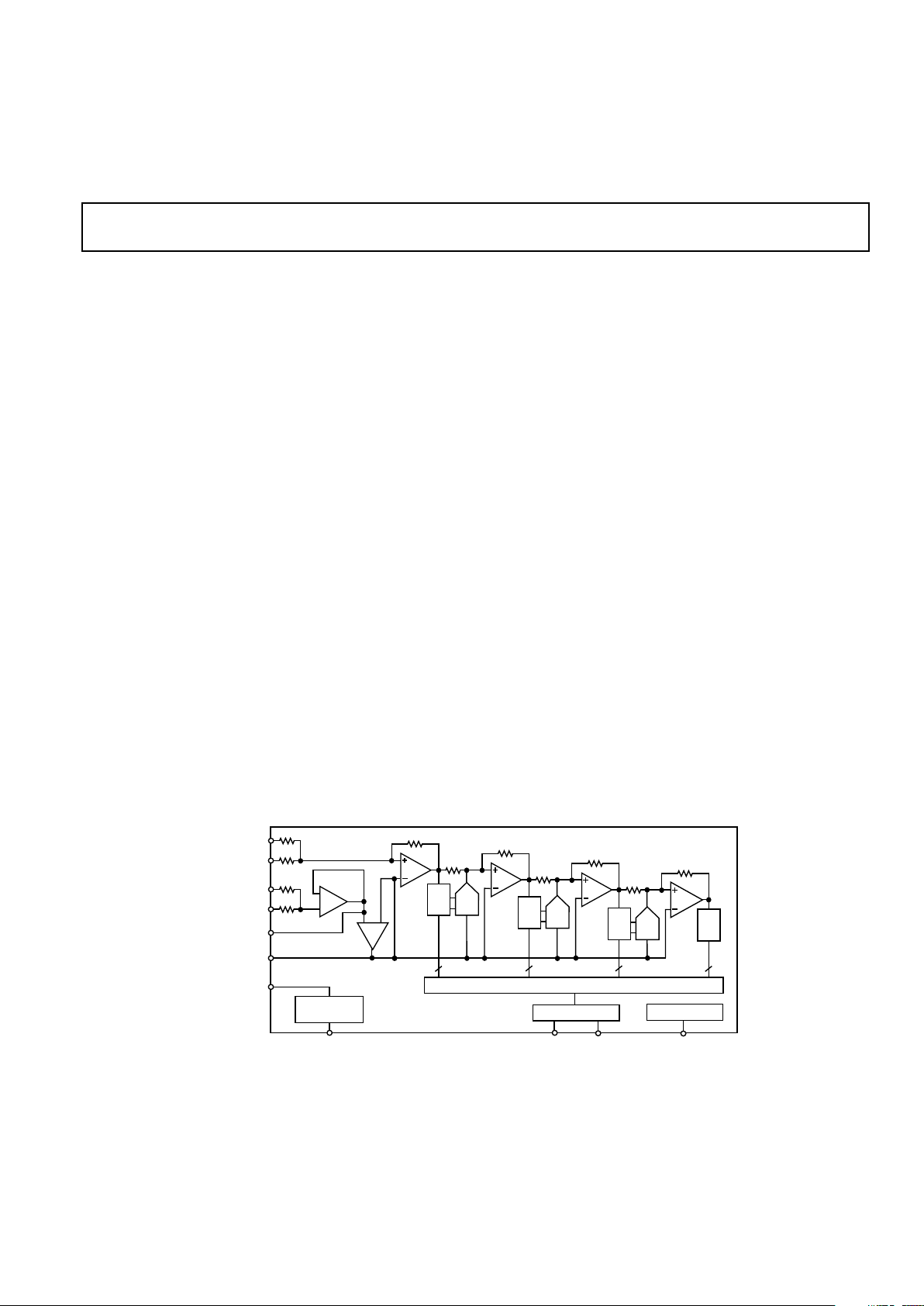
FUNCTIONAL BLOCK DIAGRAM
THA
THA
DAC
AMP
REF
AMP
4
4
3
4
CORRECTION LOGIC
2.5V REF
OUTPUT
REFCOM
OUTPUT DATA
12 BITS
CLOCK INPUT
ADC
DAC
ADC
BANDGAP
REFERENCE
LATCHES
CLOCK TIMER
NOISE
REDUCTION
AIN1 & 2
REF IN
AD1672
THA
THA
REFCOM
ADC
DAC
ADC
DAC

AD1672–SPECIFICATIONS
DC SPECIFICATIONS
REV. 0
–2–
(T
MIN
to T
MAX
with VCC = +5.0 V, VDD = +5.0 V, DRVDD = +5.0 V, f
SAMPLE
= 3 MHz unless otherwise noted)
AD1672AP
Parameter Min Typ Max Units
RESOLUTION 12 Bits
MAX CONVERSION RATE 3 MHz
ACCURACY
Integral Nonlinearity (INL) –2.5 ±1.0 2.5 LSB
Differential Nonlinearity (DNL) –1.0 ±0.5 1.5 LSB
No Missing Codes 12 Bits Guaranteed
Offset Error –0.75 ±0.20 0.75 % FSR
Zero Error
1
–0.75 ±0.20 0.75 % FSR
Gain Error
2
–1.50 ±0.30 1.50 % FSR
POWER SUPPLY REJECTION
3
VCC (5.0 V ± 0.25 V) –0.30 0.30 % FSR
V
DD
(5.0 V ± 0.25 V) –0.30 0.30 % FSR
V
DRDD
(3.0 V to 5.25 V) –0.10 0.10 % FSR
ANALOG INPUT
Input Ranges
2.5 V Range Unipolar 0.0 2.5 Volts
5.0 V Range Unipolar 0.0 5.0 Volts
5.0 V Bipolar –2.5 2.5 Volts
Input Resistance
2.5 V Input Range 1.5 2.0 2.5 kΩ
5.0 V Input Ranges 3.0 4.0 5.0 kΩ
Input Capacitance 10 pF
INTERNAL VOLTAGE REFERENCE
Output Voltage 2.475 2.5 2.525 Volts
Output Current
4
0.5 mA
REFERENCE INPUT RESISTANCE 6.0 8.0 10.0 kΩ
POWER SUPPLIES
Supply Voltages
V
CC
4.75 5.0 5.25 Volts
V
DD
4.75 5.0 5.25 Volts
DRV
DD
3.00 5.0 5.25 Volts
Supply Current
I
VCC
46 65 mA
I
VDD
1.0 2.0 mA
I
DRVDD
0.2 2.0 mA
POWER CONSUMPTION 240 363 mW
TEMPERATURE RANGE –40 25 85 °C
NOTES
1
Bipolar Mode.
2
Includes internal reference error.
3
Change in full scale as a function of the dc supply voltage.
4
Current available for external loads. External load should not change during conversion.
Specification subject to change without notice.
AC SPECIFICATIONS
AD1672AP
Parameter Min Typ Max Units
SIGNAL-TO-NOISE AND DISTORTION RATIO (S/(N+D))
f
INPUT
= 100 kHz 68 dB
f
INPUT
= 500 kHz 63 68 dB
f
INPUT
= 1.5 MHz 60 dB
SIGNAL-TO-NOISE RATIO (SNR)
f
INPUT
= 100 kHz 70 dB
f
INPUT
= 500 kHz 66 70 dB
f
INPUT
= 1.5 MHz 67 dB
TOTAL HARMONIC DISTORTION (THD)
f
INPUT
= 100 kHz –74 dB
f
INPUT
= 500 kHz –74 –64 dB
f
INPUT
= 1.5 MHz –60 dB
SPURIOUS FREE DYNAMIC RANGE (SFDR)
f
INPUT
= 100 kHz –77 dB
f
INPUT
= 500 kHz –77 –65 dB
f
INPUT
= 1.5 MHz –61 dB
INTERMODULATION DISTORTION (IMD)
1
65 dB
FULL POWER BANDWIDTH 5 MHz
SMALL SIGNAL BANDWIDTH (–20 dB FSR) 20 MHz
CODE TRANSITION NOISE 1/4 LSB rms
APERTURE DELAY 9 ns
APERTURE JITTER 10 ps rms
ACQUISITION TO FULL-SCALE STEP 150 ns
OVERVOLTAGE RECOVERY TIME 150 ns
NOTES
1
fs = 490 kHz; fb = 510 kHz typical value for third order products.
Specifications subject to change without notice.
DIGITAL SPECIFICATION
AD1672AP
Parameter Symbol Min Typ Max Units
LOGIC INPUTS
High Level Input Voltage V
IH
3.5 Volts
Low Level Input Voltage V
IL
1.0 Volts
High Level Input Current (V
IN
= VDD)IIH–10 10 µA
Low Level Input Current (V
IN
= 0 V) I
IL
–10 10 µA
Input Capacitance C
IN
10 pF
LOGIC OUTPUTS
High Level Output Voltage (I
OH
= 0.5 mA) V
OH
2.4 Volts
Low Level Output Voltage (I
OL
= 1.6 mA) V
OL
0.4 Volts
Output Capacitance C
OUT
5pF
Specifications subject to change without notice.
(T
MIN
to T
MAX
with VCC = +5 .0 V, VDD = +5.0 V, DRVDD = +5.0 V, f
SAMPLE
= 3 MHz, AIN = 0.5 dB in bipolar
–2.5 V to +2.5 V configuration unless otherwise noted)
AD1672
REV. 0
–3–
(T
MIN
to T
MAX
with VCC = +5 .0 V, VDD = +5.0 V, V
DRVDD
= +5.0 V unless otherwise noted)
AD1672
REV. 0
–4–
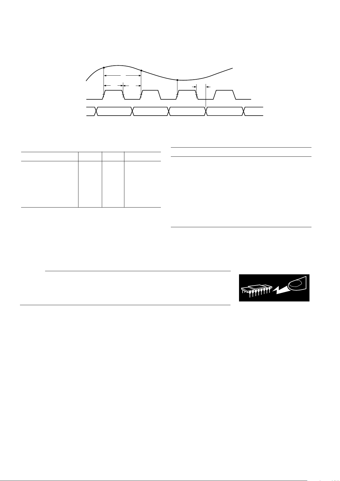
t
OD
S1
S1
S2
S2
S3
S3
DATA 1
DATA 2
ANALOG
INPUT
INPUT
CLOCK
DATA
OUTPUT
OTR
t
C
t
CL
t
CH
Figure 1. Timing Diagram
SWITCHING SPECIFICATIONS
Parameter Symbol Value Units
Clock Period t
C
334 ns min
Clock
Pulse Width High t
CH
167 ns min
Pulse Width Low t
CL
167 ns min
Output Delay t
OD
15 ns min
30 ns typ
Pipeline Delay (Latency) 2.5 Clock Cycles
ABSOLUTE MAXIMUM RATINGS*
Parameter With Respect to Min Max Units
V
CC
ACOM –0 5 +6.5 Volts
V
DD
DCOM –0.5 +6.5 Volts
DRV
DD
DRCOM –0.5 +6.5 Volts
ACOM DCOM, DRCOM –0.5 +0.5 Volts
CLOCK DCOM –0.5 V
DD
+ 0.5 Volts
Digital Outputs DCOM –0.5 DRV
DD
+ 0.5 Volts
AIN ACOM –6.5 +6.5 Volts
REFIN ACOM –0.5 V
CC
+ 0.5 Volts
Junction Temperature +150 °C
Storage Temperature –65 +150 °C
Lead Temperature (10 sec) +300 °C
*Stresses above those listed under “Absolute Maximum Ratings” may cause
permanent damage to the device. This is a stress rating only and functional
operation of the device at these or any other conditions above those indicated in the
operational sections of this specification is not implied. Exposure to absolute
maximum ratings for extended periods may effect device reliability.
WARNING!
ESD SENSITIVE DEVICE
CAUTION
ESD (electrostatic discharge) sensitive device. Electrostatic charges as high as 4000 V readily
accumulate on the human body and test equipment and can discharge without detection.
Although the AD1672 features proprietary ESD protection circuitry, permanent damage may
occur on devices subjected to high energy electrostatic discharges. Therefore, proper ESD
precautions are recommended to avoid performance degradation or loss of functionality.
AD1672
REV. 0
–5–
PIN DESCRIPTION
Pin
Symbol No. Type Name and Function
DRCOM 1 P Digital Output Driver Ground.
BIT 12 2 DO Data Bit (LSB).
BIT 2–11 3–12 DO Data Bits.
BIT 1 13 DO Data Bit (MSB).
DRV
DD
14 P +5 V Digital Output Driver Sup-
ply.
OTR 15 DO Out of Range is Active High on
the leading edge of Code 0 or the
trailing edge of Code 4096. See
Output Data Format Table V.
CLOCK 16 DI Sample Clock.
V
DD
17 P +5 V Digital Supply.
DCOM 18 P Digital Ground.
REFCOM 19, 24 P Analog Ground.
REFOUT 20 AO 2.5 V Reference Output
(Decouple with 1 µF ceramic
capacitor to REFCOM).
AIN1 21 AI Analog Input.
AIN2 22 AI Analog Input.
REFIN 23 AI Reference Input.
NCOMP2 25 AO Noise Compensation (Decouple
with 1 µF ceramic capacitor to
ACOM).
NCOMP1 26 AO Noise Compensation (Decouple
with 1 µF ceramic capacitor to
ACOM).
ACOM 27 P Analog Ground.
V
CC
28 P +5 V Analog Supply.
TYPE: AI = Analog Input; DI = Digital Input; P = Power;
AO = Analog Output; DO = Digital Output.
ORDERING GUIDE
Model Temperature Range Package
AD1672AP –40°C to +85°C P-28A
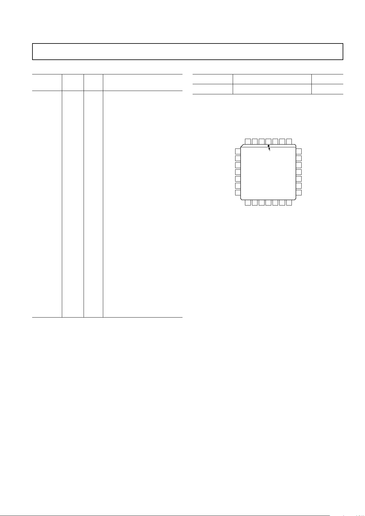
PIN CONFIGURATION
7
8
9
10
11
5
6
28 27 261234
21
22
23
24
25
19
20
121314 15 16 17 18
TOP VIEW
(Not to Scale)
PIN 1
IDENTIFIER
BIT 9
BIT 8
BIT 7
BIT 6
BIT 5
NCOMP2
REFCOM
REFIN
AIN2
AIN1
AD1672
BIT 4
BIT 3
REFOUT
REFCOM
ACOM
BIT 10
BIT 11
BIT 12 (LSB)
DRCOM
V
CC
(MSB) BIT 1
NCOMP1
BIT 2
DRV
DD
OTR
CLOCK
V
DD
DCOM

AD1672
REV. 0
–6–
DEFINITIONS OF SPECIFICATIONS
INTEGRAL NONLINEARITY ERROR (INL)
Integral nonlinearity error refers to the deviation of each individual
code from a line drawn from “negative full scale” through
“positive full scale.” The point used as “negative full scale”
occurs 1/2 LSB before the first code transition (all zeros to only
the LSB on). “Positive full scale” is defined as a level 1 1/2 LSB
beyond the last code transition (to all ones). The deviation is
measured from the middle of each particular code to the true
straight line.
DIFFERENTIAL LINEARITY ERROR (DNL, NO MISSING
CODES)
An ideal ADC exhibits code transitions that are exactly 1 LSB
apart. DNL is the deviation from this ideal value. Thus every
code must have a finite width. Guaranteed no missing codes to
12-bit resolution indicates that all 4096 codes must be present
over all operating ranges.
UNIPOLAR OFFSET ERROR
In the unipolar mode, the first transition should occur at a level
1/2 LSB above analog common. Unipolar offset is defines as
the deviation of the actual from that point.
BIPOLAR ZERO ERROR
In the bipolar mode, the major carry transition should occur for
an analog value 1/2 LSB below analog common. Zero error is
defined as the deviation of the actual transition from that point.
GAIN ERROR
The first transition should occur for an analog value 1/2 LSB
above nominal negative full scale. The last transition should
occur for an analog value 1 1/2 LSB below the nominal full
scale. Gain error is the deviation of the actual difference
between first and last code transitions and the ideal difference
between first and last code transitions.
POWER SUPPLY REJECTION
One of the effects of power supply error on the performance of
the device will be a small change in gain. The specifications
show the maximum change in the converter’s full scale as the
supplies are varied from minimum to maximum values.
APERTURE JITTER
Aperture jitter is the variation in aperture delay for successive
samples and is manifested as noise on the input to the A/D.
CODE TRANSITION NOISE
The effects of noise are to introduce an uncertainty in the precise determination of the analog input values at which the output code transitions take place, and, in effect, to increase or
reduce the quantization band. Code transition noise describes
the quantization band variation resulting from noise in terms of
rms LSBs.
APERTURE DELAY
Aperture delay is a measure of the Sample-and-Hold (SHA)
performance and is measured from the rising edge of the clock
input to when the input signal is held for conversion.
OVERVOLTAGE RECOVERY TIME
Overvoltage recovery time is defined as that amount of time
required for the ADC to achieve a specified accuracy after an
overvoltage (50% greater than full-scale range), measured from
the time the overvoltage signal reenters the converter’s range.
DYNAMIC SPECIFICATIONS
SIGNAL-TO-NOISE AND DISTORTION (S/N+D) RATIO
S/N+D is the ratio of the rms value of the measured input signal
to the rms sum of all other spectral components below the
Nyquist frequency, including harmonics but excluding dc. The
value for S/N+D is expressed in decibels.
TOTAL HARMONIC DISTORTION (THD)
THD is the ratio of the rms sum of the first six harmonic components to the rms value of the measured input signal and is
expressed as a percentage or in decibels.
INTERMODULATION DISTORTION (IMD)
With inputs consisting of sine waves at two frequencies, fa and
fb, any device with nonlinearities will create distortion products,
of order (m + n), at sum and difference frequencies of
mfa ± nfb, where m, n = 0, 1, 2, 3. . . . Intermodulation terms
are those for which m or n is not equal to zero. For example,
the second order terms are (fa + fb) and (fa – fb) and the third
order terms are (2 fa + fb), (2 fa – fb), (fa + 2fb) and (2 fb – fa).
The IMD products are expressed as the decibel ratio of the rms
sum of the measured input signals to the rms sum of the distortion terms. The two signals are of equal amplitude and the peak
value of their sums is –0.5 dB from full-scale. The IMD products are normalized to a 0 dB input signal.
FULL-POWER BANDWIDTH
The full-power bandwidth is that input frequency at which the
amplitude of the reconstructed fundamental is reduced by 3 dB
for a full-scale input.
SPURIOUS FREE DYNAMIC RANGE
The difference, in dB, between the rms amplitude of the input
signal and the peak spurious signal.

AD1672
REV. 0
–7–
Sample Rate: 3 MSPS and AIN = –0.5 dB
CODE
1.0
–1.0
0 4000500
DNL ERROR – LSB
1000 1500 2000 2500 3000 3500
0.8
0.2
–0.2
–0.6
-0.8
0.6
0.4
0.0
–0.4
Figure 2. Typical DNL Performance
INPUT FREQUENCY – Hz
S/(N+D) – dB
80
40
10
5
10
7
10
6
75
70
–0.5dB
– 6.0dB
60
55
50
45
65
– 20.0dB
Figure 3. S/(N+D) vs. Input Frequency
INL ERROR – LSB
CODE
2.5
–2.5
0 4000500 1000 1500 2000 2500 3000 3500
2.0
0.5
–0.5
–1.5
–2.0
1.5
1.0
0.0
–1.0
Figure 4. Typical INL Performance
AMPLITUDE – dB
70
58
–10 0–7
68
60
–5
62
64
66
S/(N+D) – dB
–9 –8 –6 –4 –3 –2 –1
500kHz
1.5MHz
1MHz
Figure 5. S/(N+D) vs. Amplitude
INPUT FREQUENCY – Hz
AMPLITUDE – dB
–40
–50
–90
10
5
10
7
10
6
–60
–70
–80
THD
2nd HARM
3rd HARM
Figure 6. Distortion vs. Input Frequency, Full-Scale Input
Typical Performance Characteristics–AD1672
REV. 0
–7–

Sample Rate: 3 MSPS and AIN = –0.5 dB
15dB/DIV
1
3
4
5
78
9
6
2
THD = –74.42dB
S/(N+D) = 68.83dB
SFDR = –78.79dB
HARMONICS – dB
2ND –79 6TH –86
3RD –86 7TH –93
4TH –78 8TH –95
5TH –81 9TH –96
Figure 7. Typical FFT, fIN = 525 kHz
AD1672–Dynamic Characteristics
REV. 0
–8–
15dB/DIV
1
3
4
5
7
8
9
6
THD = –60.12dB
S/(N+D) = 59.70dB
SFDR = –61.09dB
HARMONICS – dB
2ND –61 6TH –79
3RD –67 7TH –91
4TH –98 8TH –93
5TH –78 9TH –87
2
Figure 8. Typical FFT, fIN = 1.450 MHz
THEORY OF OPERATION
The AD1672 is implemented using a 4-stage pipelined multiple
flash architecture. The flash resolution for the stages is 4-4-3-4
with one-bit of overlap used between stages for error correction.
A low noise sample-and-hold amplifier (SHA) acquires a fullscale, single-ended input to 12-bit accuracy within 167 ns. A
4-bit approximation of the input is made by the first flash converter, and an accurate analog representation of this four-bit estimate is generated by a digital-to-analog (DAC) converter.
This approximation is subtracted from the SHA output to produce a remainder, or residue. This residue is then sampled and
held by the second SHA, and a 4-bit approximation is generated
and subtracted by the second stage. Once the second SHA goes
into hold, the first stage goes back into sample mode to acquire a
new input signal.
The third stage which has 3 bits of resolution is similar to the
first and second stage in that each stage consists of a SHA, flash
ADC, and a DAC. Each stage preforms a 4- (or 3-) bit approximation/subtraction operation with the residue of each stage
being passed on to the next stage. The fourth or last stage consists only of a 4-bit flash ADC which converts the final residue.
The 15 output bits from the 4 flash converters are accumulated
in the correction logic block, which adds the bits together using
the appropriate correction algorithm, to produce the 12 bit
output word. The digital output, together with the overrange
indicator (OTR), is latched into an output buffer to drive the
output pins.
The additional SHA inserted in each stage of the AD1672 architecture allows pipelining of the conversion. In essence, the converter is converting multiple inputs simultaneously, processing
them through the converter chain serially. This means that
while the converter is capable of capturing a new input sample
every clock cycle, it actually takes 2 1/2 clock cycles for the conversion to be fully processed and appear at the output. This
“pipeline delay” is often referred to as latency, and is not a concern in most applications, however there are some cases where it
may be a consideration. For example, some applications call for
the A/D converter to be placed in a high speed feedback loop,
where its input is servoed to provide a desired result at the digital output (e.g., offset calibration or zero restoration in video
applications). In these cases the clock cycle delay through the
pipeline must be accounted for in the loop stability calculations.
Also, because the converter is working on three conversions simultaneously major disruptions to the part (such as a large
glitch on the supplies or reference) may corrupt three data
samples. Finally, there will be a minimum clock rate below
which the SHA droop corrupts the signal in the pipeline. In the
case of the AD1672, this minimum clock rate is 20 kHz at
25°C.
The AD1672 clock circuitry uses both edges of the clock in its
internal timing circuitry (see specification page for exact timing
requirements). The AD1672 samples the analog input on the
rising edge of the clock input. During the clock low time (between the falling edge and rising edge of the clock), the input
SHA is in sample mode; during the clock high time it is in hold.
System disturbances just prior to the rising edge of the clock
may cause the part to acquire the wrong value, and should be
minimized. While the part uses both clock edges for its timing,
jitter is only a significant issue for the rising edge of the clock
(see CLOCK INPUT section).

AD1672
REV. 0
–9–
APPLYING THE AD1672
ANALOG INPUTS
Figure 9 shows the equivalent analog input of the AD1672. The
input SHA and associated resistor network topology can be easily configured for either unipolar (0 V to 2.5 V, 0 V to 5.0 V) or
bipolar (–2.5 V to 2.5 V) input signals as shown in Figure 10.
The nominal input resistance, R
IN
, of the AD1672 is 2 kΩ for a
2.5 V span and 4 kΩ for a 5 V span. The circuit topology both
level shifts and inverts the analog input for the various input
spans.
SHA
OUT
AIN 1
4kΩ
2kΩ
V
BIAS
1.25V
4kΩ
AIN 2
2kΩ
Figure 9. Equivalent Analog Input Circuit
21
22
20
23
1µF
AIN1
AIN2
REFOUT
REFIN
AD1672
V
IN
21
22
20
23
1µF
AIN1
AIN2
REFOUT
REFIN
AD1672
V
IN
21
22
20
23
1µF
AIN1
AIN2
REFOUT
REFIN
AD1672
V
IN
a. 0 to +2.5 V Input Range b. 0 to +5.0 V Input Range
c. –2.5 to +2.5 V Input Range
Figure 10. Input Range Connections
In applications where ac coupling of the analog input signal is
appropriate such as in a single supply system, the user can
capacitively couple the input signal for a 2.5 V or 5 V span thus
removing any preceding system dc offsets. Figure 11 shows the
proper configurations of the AD1672 for ac coupling. Maintaining the specifications outlined in the data sheet requires careful selection of the component values. The most important
concern is that the f
–3 dB
high pass corner is a function of C1 and
C2 in parallel with R
IN
. The f
-3 dB
point can be approximated
by the equation
/
f
–3 dB
=1/(2×π×RIN×C
EQ
)
where CEQ is the parallel combination of C1 and C2. Note that
C1 is typically a large electrolytic or tantalum capacitor that becomes inductive at high frequencies. Adding a small ceramic
capacitor on the order of 0.1 µF that does not become inductive
until negligibly higher frequencies maintains a low impedance
over a wide frequency range.
21
22
25
20
23
C1
10µF
C2
1.0µF
10µF
1.0µF
ANALOG
INPUT
AIN1
AIN2
NCOMP2
REF
OUT
REFIN
AD1672
21
22
25
20
23
C1
10µF
C2
1.0µF
10µF
1.0µF
ANALOG
INPUT
AIN1
AIN2
NCOMP2
REF
OUT
REFIN
AD1672
2.5V Span 5.0V Span
Figure 11. AC Coupled Inputs
In applications requiring dc coupling, a buffer amplifier is recommended for driving the AD1672 input. Any source resistance will contribute to both gain and offset error due to its
interaction with the AD1672’s input resistance. The particular
application and signal input range will determine how the buffer
amplifier is configured. For example, in dc precision applications, the buffer amplifier can be configured for convenient gain
and offset adjustment as shown in Figure 12. In spectral
analysis/signal processing applications, the buffer amplifier can
be configured as a 2nd order antialiasing filter in a Sallen-Key
or Multiple-Feedback topology as shown in Figure 13.
V
CC
500Ω 50Ω 500Ω
5kΩ
50Ω
5kΩ
0.1µF
V
EE
ANALOG
INPUT
OFFSET
ADJUSTMENTS
GAIN
ADJUSTMENT
AD1672
AIN
Figure 12. Offset and Gain Adjustment
V
IN
V
OUT
C2
R4
C1
R2R1
R3
V
IN
V
OUT
C2
C1
R2R1
R3
Figure 13. Sallen-Key and Multiple-Feedback
Antialiasing Filter Topologies
In imaging and multiplexed data acquisition applications, the
AD1672’s wide input bandwidth facilitates rapid acquisition of
transient input signals: the input SHA can typically settle to 12bit accuracy from a full scale input step in less than 150 ns. Figure 14 illustrates the typical acquisition of a full scale input step.
For amplifiers that are powered by supplies greater than
6.5 V, it is recommended that a clamping circuit be included at
the input of AD1672. This circuit limits the input voltage to
6.5 V under a fault condition.

AD1672
REV. 0
–10–
The selection of the buffer is of particular concern in preserving
the performance of the AD1672. The total output referrednoise contribution of the selected amplifier should be less than
200 µV rms to preserve the AD1672’s noise performance. The
amplifiers harmonic distortion should be 12 dB or better in performance than the AD1672 over the bandwidth and signal level
range of the particular application. The selected amplifier
should settle to 0.01% within 70 ns.
Table I lists the performance of various suitable amplifiers when
configured for a gain of +1 or –1 with the AD1672 configured
for ±2.5 V bipolar operation and f
CLOCK
= 3 MHz. The AD80xx
family of high speed amplifiers are only suitable for ±2.5 V
bipolar and 0 V–2.5 V unipolar operation due to their powersupply range and voltage output swing constraints. Note that
the SNR, THD, and SFDR results in Tables I, II and III are for
a 750 kHz full-scale (–0.5 dB) input signal. These results were
determined experimentally using the AD1672 evaluation board,
and hence the stated amplifier’s performance is inclusive of the
AD1672.
Table I. –2.5 V to +2.5 V Range
ADI
Part # SNR THD SFDR Gain
AD8047 70.5 –67.5 –68.4 +1
AD8041 70.0 –67.3 –68.2 +1
AD8011 70.5 –67.0 –67.8 +1
AD817 70.4 –62.1 –62.9 +1
AD818 70.3 –65.0 –68.0 –1
AD811 70.3 –61.9 –63.4 +1
w/o Op Amp 70.5 –67.5 –68.4
Table II lists the performance of three high speed amplifiers
which are configured for a gain of +1 or –1 with the AD1672
configured for 0 V to 5 V unipolar operation and f
CLOCK
= 3 MHz.
Note that these amplifiers may operate at the higher power supply range to achieve the 0 V to 5 V output swing.
Table II. 0 V to +5 V Range
Settling
ADI Time (ns)
Part # SNR THD to 0.01% Gain
AD811 70.1 –67.6 65 +1
AD817 70.1 –68.9 70 +1
AD818 70.0 –67.4 80 –1
Table III lists the performance of two high speed amplifiers
specified for single supply operation. They are configured for
a gain of +1 with the AD1672 configured for 0 V to 2.5 V
unipolar operation and f
CLOCK
= 3 MHz. The output of these
amplifiers are ac coupled to the AD1672.
Table III. AC Coupled 0 V to 2.5 V Range
ADI
Part # SNR THD SFDR
AD8011 70.1 –70.0 –71.6
AD8041 69.7 –71.3 –73.4
nsec
0 16020 40 60 80 100 120 140
4500
4000
0
2000
1500
1000
500
3000
2500
3500
CODE OUT
Figure 14. Typical AD1672 Settling Time
The AD1672 will contribute its own wideband thermal noise.
As a result of the integrated wideband noise (1/4 LSB rms,
referred-to-input), applying a dc analog input produces more
than one code at the output. A histogram analysis of the
AD1672 with a dc input is shown in Figure 15. It shows a bell
shaped curve consistent with the Gaussian nature of the thermal
noise. This histogram will be approximately 3 codes wide,
depending on how well the input is centered on a given code
and how many samples are taken. Figure 16 illustrates the
AD1672’s transition noise.
DEVIATION FROM CORRECT CODE – LSB
2100000
1800000
0
1200000
900000
600000
300000
1500000
+1–1 0
# CODE HITS
2015807
13639
67324
Figure 15. Typical Grounded Histogram
100
90
0
60
30
20
10
80
70
40
50
100 x p (≥ CODE X + 1)
σ = 0.25 LSB RMS
CODE X CODE X ÷ 1
Figure 16. Code Probability at a Transition

AD1672
REV. 0
–11–
REFERENCE INPUT
The nominal reference input is 2.5 V, taken with respect to
REFCOM. The reference input pin (REFIN) can be connected
to the reference output pin (REFOUT) or a standard external
+2.5 Volt reference can be selected to meet specific system requirements. Figure 17 shows the AD1672’s REFIN being
driven from an external precision voltage reference such as the
REF192. If an external reference is used, REFOUT can be effectively disabled by tying it directly to the positive supply voltage V
CC
. Note that if the reference is changed during a conversion,
all three conversions in the pipeline will be invalidated.
The nominal 2.5 V reference input is rescaled to 1.25 V via a
resistor divider network as shown in Figure 18. The nominal
resistance of this resistor network is 8 kΩ. Table IV summarizes various 2.5 V references for use with the AD1672 (see
REFERENCE OUTPUT section).
Table IV. Suitable 2.5 Volt References
Drift Initial Accuracy
(ppm/8C) %
REF43B 10 (max) 0.1
REF192E 5 (max) 0.08
AD780B 3 (max) 0.04
0.1µF10µF
+V
CC
+V
CC
AD780
OUTPUTGND
V
S
1µF
AD1672
REFIN
REFOUT
Figure 17. Circuit using AD780 Optional +2.5 V
Reference Input Circuit
REFERENCE NOISE REDUCTION
Figure 18 shows the proper connection of two external 1 µF
capacitors, C
NR1
and C
NR2
, associated with the two noise re-
duction nodes NCOMP1 and NCOMP2 (Pins 25 and 26) of
the AD1672. Although these noise reduction capacitors, CNR, are
not required for stability, the most optimum noise and distortion performance will be attained with a 1
µ
F ceramic capacitor connected
from each Noise Reduction node to ACOM. C
NR1
is associated with
the output of the DAC amp and is required for optimum distortion performance and SHA settling time. It provides a low
source impedance for signal-dependent, transient currents associated with this node. C
NR2
reduces the noise contribution from
the reference buffer amplifier.
CNR2
1µF
1µF
CNR1
1µF
NCOMP2
REFOUT
REFIN
AD1672
REFCOM
NCOMP1
DAC
AMP
REF
AMP
4kΩ
4kΩ
20
23
24
25
26
Figure 18. Reference Noise Reduction
REFERENCE OUTPUT
The AD1672 includes an onboard +2.5 V curvature compensated bandgap reference that has been laser trimmed for both
absolute value and temperature drift. The reference must be
externally compensated with a capacitor of 1 µF or greater from
REFOUT to REFCOM.
The reference is specified to provide an additional load current
up to 500 µA. For large dynamic loads and/or external loads
greater than 500 µA, an external buffer amplifier or pull-up re-
sistor is required. If a pull-up resistor is used, its value should
be selected such that REFOUT will not be required to sink any
current under all operating conditions. Figure 19 illustrates the
load regulation of the reference. The power supply rejection of
the reference is better than 0.2 % of FSR at dc.
LOAD CURRENT – µA
REFERENCE VOLTAGE – Volts
2.500
2.493
2.490
0 100 200 300 400 500 600 700 800 900 1000
2.499
2.494
2.492
2.491
2.498
2.496
2.497
2.495
Figure 19. Reference Output Voltage vs. Load Current
DIGITAL OUTPUTS
The AD1672 output data is presented in positive true straight
binary for both the 0 V to 2.5 V and 0 V to 5 V unipolar input
ranges and positive true offset binary for the ± 2.5 V bipolar
range. Table V indicates the output data formats for the three
analog input ranges. Users requiring twos complement encoding
for the ±2.5 V range may simply invert the MSB (Pin 13).
Table V. Output Data Format
Input Voltage Range +FS (V) –FS (V) LSB (mV)
0 to +2.5 +2.5 0.0 0.610
0 to +5.0 +5.0 0.0 1.22
–2.5 to +2.5 +2.5 –2.5 1.22
–FS+1/2 LSB
–FS
–FS –1/2 LSB
+FS
+FS –1/2 LSB
OTR
+FS –1 1/2 LSB
OTR DATA OUTPUTS
1 1111 111 1111
0 1111 1111 1111
0 1111 1111 1110
0 0000 0000 0001
0 0000 0000 0000
1 0000 0000 0000
Figure 20. Output Data Format

AD1672
REV. 0
–12–
The AD1672’s CMOS digital output drivers can be configured
to interface with +5 V or +3.3 V logic families by setting
DRV
DD
to +5 V or +3.3 V respectively . They are also sized to
provide sufficient output current to drive a wide variety of logic
families. However, large drive currents tend to cause glitches
on the supplies and may effect S/(N+D) performance. Applications requiring the AD1672 to drive large capacitive loads or
large fanout may require additional decoupling capacitors on
DRV
DD
and DVDD. In extreme cases, external buffers or
latches may be required.
OUT OF RANGE
An out-of-range condition exists when the analog input voltage
is beyond the input range (0 V to +2.5 V, 0 V to +5.0 V, ±2.5 V)
of the converter. OTR (Pin 15) is a digital output which is updated along with the data output pertaining to the particular
sampled analog input voltage. Hence, OTR has the same pipeline delay (latency) as the digital data. It is set low when the
analog input voltage is within the analog input range. It is set
HIGH and will remain HIGH when the analog input voltage
exceeds the input range by typically 1/2 LSB from the center of
the ±full-scale output codes. OTR will remain HIGH until the
analog input is within the input range and another conversion is
completed. By logical ANDing OTR with the MSB and its
complement, overrange high or underrange low conditions can
be detected. Table IV is a truth table for the over/under range
circuit in Figure 20 which uses NAND gates. Systems requiring programmable gain conditioning prior to the AD1672 can
immediately detect an out-of-range condition, thus eliminating
gain selection iterations. Also, OTR can be used for digital offset and gain calibration (see Gain and Offset Adjustment).
Table VI. Out-of-Range Truth Table
OTR MSB Analog Input Is
0 0 In Range
0 1 In Range
1 0 Underrange
1 1 Overrange
OVER = “1”
UNDER = “1”
MSB
OTR
LSB
Figure 21. Overrange or Underrange Logic
CLOCK INPUT
The AD1672 internal timing control uses the two edges of the
clock input to generate a variety of internal timing signals. The
clock input must meet or exceed the minimum specified pulse
width high and low (t
CH
and tCL) specifications of 167 ns to
maintain the AD1672’s rated performance. At a clock rate of
3 MSPS, the clock input must have a 50% duty cycle to meet
this timing requirement. For clock rates below 3 MSPS, the
duty cycle may deviate from 50% to the extent that both tch and
tcl are satisfied. One way to minimize the tolerance of a 50%
duty cycle clock is to divide down a clock of higher frequency,
as shown in Figure 22.
6MHz
CLK
3MHz
+5V
R
Q
Q
D
S
+5V
Figure 22. Divide-by-Two Clock Circuit
In this case, a 6 MHz clock is divided by 2 to produce the 3 MHz
clock input for the AD1672. In this configuration, the duty
cycle of the 6 MHz clock is irrelevant.
The input circuitry for the CLOCK pin is designed to accommodate CMOS inputs. The quality of the logic input, particularly the rising edge, is critical in realizing the best possible jitter
performance for the part: the faster the rising edge, the better
the jitter performance.
The offset of the AD1672 is sensitive to the rising edge (i.e.,
dV/dt) seen at CLOCK due to clock feedthrough. An additional offset component becomes noticeable for rise times below
10 ns and causes an additional few LSBs of offset. The amount
of additional offset is dependent on dV/dt of the rising edge and
hence will remain constant for nonvarying rising edges. For
applications which are sensitive to a change in offset due to a
variation in the rise edge, the CLOCK rise time may be reduced
by selecting a slower logic family or installing a 1 kΩ resistor between the clock driver and CLOCK of the AD1672.
As a result, careful selection of the logic family for the clock
driver, as well as the fanout and capacitive load on the clock
line, is important. Jitter-induced errors become more predominant at higher frequency, large amplitude inputs, where the
input slew rate is greatest.
Although the AD1672 is designed to support a sampling rate of
3 MSPS, operating at slightly faster or slower clock rates may be
possible with a minimum degradation in performance levels. Figure 23 is a plot of the S/(N+D) vs. clock frequency for a 500 kHz
analog input. In fact, the AD1672 is capable of operating with
a clock frequency as low as 20 kHz
FREQUENCY – MHz
75
70
50
050.5
S/(N+D) – dB
1 1.5 2 2.5 3 3.5 4 4.5
65
60
55
Figure 23. Typical S/(N+D) vs. Clock Frequency;
f
IN
= 500 kHz, Full-Scale Input

AD1672
REV. 0
–13–
The power dissipated by the correction logic and output buffers
is largely proportional to the clock frequency; running at reduced
clock rates provides a slight reduction in power consumption.
Figure 24 illustrates this tradeoff.
FREQUENCY – MHz
260
252
244
250
248
246
258
256
254
050.5
POWER – mW
1 1.5 2 2.5 3 3.5 4 4.5
Figure 24. Typical Power Dissipation vs. Clock Frequency
GROUNDING AND POWER SUPPLY DECOUPLING
RULES
Proper grounding and decoupling should be a primary design
objective in any high speed, high resolution system. The AD1672
features separate analog and digital supply and ground pins to
optimize the management of analog and digital ground currents
in a system. In general, V
CC
, the analog supply, should be decoupled to ACOM, the analog common, as close to the chip as
physically possible. Similarly, V
DD
, the digital supply, should be
decoupled to DCOM as close to the chip as physically as possible. DRV
DD
, the digital supply for the output drivers should
be decoupled to DRCOM which is also connected to the digital
ground plane.
Figure 31, the AD1672/EB evaluation board schematic, demonstrates the recommended decoupling strategy for the supply
pins. Note that in extremely noisy environments, a more elaborate supply filtering scheme may be necessary. Figure 25 shows
the power supply rejection ratio vs. frequency for 100 mV of
FREQUENCY – MHz
1100.2
SUPPLY REJECTION – dB
2
–30
–120
–40
–50
–60
–70
V
CC
V
DD
DRV
DD
–80
–90
–100
–110
0.1 0.5
5
Figure 25. Power Supply Rejection vs. Frequency,
100 mV p-p Signal on Power Supplies
FREQUENCY – MHz
0.1 100.2 2
75
65
60
55
40
50
45
70
DRV
DD
V
CC
V
DD
510.5
S/(N+D) – dB
Figure 26. S/(N+D) vs. Supply Noise Frequency
power supply ripple at various frequencies. Figure 26 shows the
degradation in S/(N+D) ratio resulting from this 100 mV power
supply ripple for a full-scale analog input at 500 kHz. The
AD1672/EB evaluation board was used to generate these graphs
The AD1672 is designed to minimize the code dependent current at REFCOM, therefore reducing input dependent analog
ground voltage drops and errors. The majority of code dependent ground current is diverted to ACOM.
The digital activity on the AD1672 chip falls into two general
categories: CMOS correction logic, and CMOS output drivers.
The internal correction logic draws relatively small surges of
current which flow through V
DD
and DCOM. The output
drivers draw large current impulses while the output bits are
changing. The size and duration of these currents is a function
of the load on the output bits: large capacitive loads are to be
avoided. The output drivers are supplied through DRV
DD
and
DRCOM. A 0.1 µF ceramic capacitor for decoupling the driver
supply, DRV
DD
, is appropriate for a reasonable capacitive load
on the digital outputs (typically 20 pF on each pin). Applications involving greater digital loads should consider increasing
the digital decoupling proportionately.
For those applications that require a single +5 V supply for both
the analog and digital supply, a clean analog supply may be
generated using the circuit shown in Figure 27. The circuit
consists of a differential LC filter with separate power supply
and return lines. Lower noise can be attained using low ESR
(Equivalent Series Resistance) type electrolytic and tantalum
capacitors.
FERRITE
BEADS
100µF
ELECT.
10–20µF
TANT.
0.1µF
CER.
+5V
AGND
+5V DGND
+5V
POWER SUPPLY
TTL/CMOS
LOGIC
CIRCUITS
Figure 27. Differential LC Filter for Single +5 V Applications

AD1672
REV. 0
–14–
GAIN AND OFFSET ADJUSTMENT
The AD1672 is factory trimmed to minimize gain, offset and
linearity errors. In some applications, the gain and offset errors
need to be externally trimmed to zero. Since the gain and offset
errors of the AD1672 are interdependent, an iterative process is
required to trim both errors. The OTR pin can be monitored to
trim the offset and gain errors to within 1/2 LSB of negative and
positive full-scale (i.e., –FS and +FS) respectively. In this case,
the calibration procedure would be to iterate between –FS and
+FS voltage levels which are applied to the input of the AD1672
and adjust the offset and gain until OTR toggles at both –FS
and +FS.
Both gain and offset errors may be trimmed with external calibration circuits based on a potentiometer or a DAC. Digital
calibration circuits using a DAC offers greater flexibility and
can be programmed for various operating conditions. The following digital calibration circuits are based on the DAC08
which is a low cost, 8-bit current output DAC with 85 ns settling time performance. Different adjustment spans and resolution may be achieved by judicious selection of the resistors in
the circuit.
Figure 28 shows an offset correction circuit for the unipolar
input ranges of 0 V to 2.5 V and 0 V to 5.0 V. The complementary current outputs of the DAC08 provide a bipolar adjustment
range at the output of the op amp if R
S
is made equal to RF/G.
G is the noninverting gain of the op amp and is equal to
1 + R
F/RA
. REFOUT divided by RIN sets the full-scale current
output, I
FS
, for the DAC08 Note, RP is a pull-up resistor used
to source additional current if I
FS
is greater than 500 µA. The
bipolar voltage adjustment span at the output of the op amp is
equal to I
FS
× RF. RI isolates the op amp from the DAC08
output capacitance. Note, that the values of these resistors can
be optimized for any circuit requirement or adjustment span
since they are not uniquely defined for any given voltage span.
R
F
R
A
R
I
R
I
V
REF(+)
V
REF(–)
DAC08
I
O
I
O
R
IN
RIN1µF
R
P
AD1672
AIN
REFOUT
+V
CC
Figure 28. Unipolar Offset Correction Using the DAC08
Figure 29 shows an offset correction circuit for the bipolar input
range of –2.5 to +2.5 V. This circuit is similar to the circuit
shown in Figure 28 except that the op amp is configured in an
inverting topology so that the voltage compliance of the DAC08
is not exceeded.
R
F
R
A
R
I
R
I
V
REF(+)
V
REF(–)
DAC08
I
O
I
O
R
IN
RIN1µF
R
P
+V
CC
R
S
AD1672
AIN
REFOUT
Figure 29. Bipolar Offset Correction Using the DAC08
Figure 30 shows a gain correction circuit which is also similar to
the circuit shown in Figure 28. The circuit consists of a unity
gain amplifier in which R
S
and RF are equal to 158 Ω. In this
case, the full-scale output current of the DAC08, I
FS
, is set at
500 µA to minimize the load to the AD1672 REFOUT. The
output of the op amp can be varied over a ±78 mV range
around the midscale voltage of REFOUT. Also, R
S
and RF are
selected such that 1 LSB of the DAC08 corresponds to 1 LSB
of the AD1672.
500Ω
5kΩ
5kΩ
1µF
4.7kΩ
+V
CC
AD1672
REFIN
REFOUT
2.5V
V
REF(+)
V
REF(–)
DAC08
I
O
I
O
500Ω
158Ω
158Ω
2.5 ±0.078V
Figure 30. Gain Correction Using the DAC08
OUTPUT LATCHES
The AD1672/EB evaluation board schematic in Figure 31
shows the AD1672 connected to the 74HC541 octal/buffer line
drivers with three-state outputs. The latch can drive highly capacitive loads (i.e., bus lines, I/O ports) while maintaining the
data signal integrity.
AD1672 EVALUATION BOARD GENERAL DESCRIPTION
The AD1672/EB is an evaluation board for the AD1672 12-bit
3 MSPS analog-to-digital converter (ADC). Figure 31 shows the
schematic for the AD1672/EB evaluation board. Careful attention
to layout and circuit design combined with analog and digital prototyping areas allows the user to easily and effectively evaluate the
AD1672 in any application requiring high resolution, high speed
conversion.
The analog input to the AD1672/EB may be driven directly or
via an onboard buffer amplifier. The AD1672/EB contains an
8-bit DAC which can be easily configured for input offset adjustment or for reconstruction of the digital output. An optional
external voltage reference is included for greater dc precision

AD1672
REV. 0
–15–
and/or offset adjustment purposes. Onboard data buffers are
also included. The AD1672/EB requires an external clock
which is applied from a user’s bench or generated from a circuit
built on the prototyping area. A standard 40-pin IDC-connector
provides access for the digital outputs from the AD1672/EB. The
user must also provide a digital +5 V power supply and analog
±5 V supplies to operate the AD1672/EB.
OPERATING PROCEDURE AND FUNCTIONAL
DESCRIPTION
Power
Apply power to the AD1672/EB by attaching banana plugs to
the appropriate banana jacks on the printed circuit board (Figure 31). The +V
CC
analog supply should be +5 V (± 5%) and
be capable of supplying 70 mA. The –V
EE
analog supply should
be –5 V (±5%) and be capable of supplying 20 mA. The +V
DD
digital supply should be +5 V (± 5%) and be capable of supplying 12 mA (not including any additional current required by the
digital load).
The power supply pin for the onboard output drivers internal to
the AD1672 (DRV
DD
–Pin 14) can be driven directly by the
digital supply, +V
DD
, by installing JP10 or may be driven via a
separate supply by removing JP10 and driving the test point,
TP5. The separate supply option allows the user to interface
with +5 V or +3.3 V (±5%) logic families.
JP1 To provide +V
CC
supply to both U3 (DAC08) and U1
(op amp), attach jumper JP1.
JP10 To provide +5 V (+/-5%) supply to DRV
DD
pin of
AD1672 via +V
DD
or separate supply. To provide power
to DRV
DD
pin via +VDD, install JP10. To provide power
to DRV
DD
pin via separate supply, remove JP10 and con-
nect external supply to test point TP5.
Analog Inputs
The BNC jack, AIN (J1), accepts voltage inputs that comply
with the analog input requirements of the AD1672. It is terminated with a 49.9 Ω resistor (R1) located on the componentside of the evaluation board. Remove and/or replace this
resistor with other values in order to match different cable impedances. The AD1672 analog input can be directly driven via
AIN (J1) by installing JP2 and removing JP3 or it can be driven
via an amplifier (U1) by installing JP3 and removing JP2. The
amplifier (U1) may be configured in the inverting or noninverting mode with a gain of one by configuring S4.
JP2 Installing JP2 and removing JP3, directly dc couples AIN
(J1) to the AD1672 analog input.
JP3 Installing JP3 and removing JP2, indirectly dc couples
AIN (J1) to the AD1672 analog input via the inverting
op amp U1.
S4 Selects inverting or noninverting gain of one for the am-
plifier U1. When S4 is in position A, the noninverting
mode is selected. When S1 is in position B, the inverting
mode is selected.
The AD1672’s analog input range can be configured for
0 V–2.5 V, 0 V–5 V, or ± 2.5 V by installing only one of the four
jumpers, JP5–JP7, as outline in Table VII.
JP5 Installing only jumper JP5, the 0 V–2.5 V range of the
AD1672 is selected.
JP6 Installing only jumper JP6, the 0 V–5 V range of the
AD1672 is selected.
JP7 Installing only jumper JP7, the ±2.5 V range of the
AD1672 is selected.
Table VII. Analog Input Range Selection
Analog Input Range
(Volts) JP5 JP6 JP7
0 to 2.5 ON OFF OFF
0 to 5.0 OFF ON OFF
±2.5 OFF OFF ON
Reference
An external 2.5 V voltage reference, U2, is also included on the
AD1672/EB to provide the option for greater dc precision than
the AD1672’s internal reference. The external reference also
provides the proper biasing currents for the offset adjustment
circuitry consisting of U3. To use the external voltage reference
for the AD1672, install JP9 and remove JP4. To use the AD1672’s
internal voltage reference, install JP4 and remove JP9.
JP4 Installing JP4 and removing JP9 selects the AD1672’s
internal reference.
JP9 Installing JP9 and removing JP4 selects the external
reference, U2.
Offset Adjustment/Reconstruction DAC
An 8-bit complementary current output DAC08, U3, allows for
either offset adjustment of the analog input or reconstruction of
the AD1672 digital output for simple evaluation purposes. The
offset adjustment option is implemented by installing both JP3
and JP8. Note that JP5, JP6 and JP7 should be removed so
that the AD1672 is configured for a 0 V–5 V range.
The DAC08 can also be configured to reconstruct the digital
output of the AD1672 using its digital output for the DAC08’s
digital input. The output of the user supplied ribbon cable used
to interface with the 40-pin IDC connector (E1) can be connected directly to the connector U8, hence recirculating the
eight most significant digital output bits of the AD1672. In this
configuration, JP8 would be removed and the reconstructed
waveform (±50 mV p-p) can be monitored via test point TP4.
JP8 Installing JP8 and removing JP5, JP6 and JP7 selects the
offset adjustment option. Removing JP8 and connecting
E1 to U8 via an external user-supplied ribbon cable
selects the reconstruction option.

AD1672
REV. 0
–16–
Clock Input
A 49.9 Ω resistor (R9) terminates this input. Remove and/or
replace this resistor with other values in order to match different
cable impedances. An external sample clock must be provided
to the BNC connector labeled CLK (J5). The rising or falling
edge of CLK can be selected to trigger a conversion and is available to the user via the connector E1 by configuring S1 and S3.
The CLK INPUT has two modes of operation which is
determined by the position of S5. When S5 is in Position B, the
CLK is directly coupled to U5, a Hex inverter with Schmitt trigger inputs. The requisite input levels are CMOS-compatible in
this mode. When S5 is in Position A, the CLK is ac coupled via
C23 and level shifted via R10, R12, and R13. This mode is
used to generate a low jitter clock input for the AD1672 with a
tunable duty cycle. The input to CLK (J5) is a filtered 5 V p-p
sine wave at the desired sampling frequency. The duty cycle
may be adjusted via R10.
S1 Selects the rising or falling edge of CLK to initiate a con-
version. When S1 is in Position A, the falling edge of
CLK is selected. When S1 is in Position B, the rising
edge of CLK is selected.
S3 Selects the rising or falling edge of CLK made available to
the user via the connector via E1, Pin 33. When S3 is in
Position A, the rising edge of CLK is selected. When S1
is in Position B, the falling edge of CLK is selected.
S5 Selects CLK INPUT mode of operation. If S5 is in Posi-
tion A, the low jitter, ac coupled mode of operation is selected. If S5 is Position B, the dc coupled mode
of operation is selected.
Digital Inputs/Outputs
The digital outputs of the AD1672 are buffered and connected
to a 40-pin IDC connector (E1). The digital output can be either in a straight binary or twos complement format by configuring S2. S2 selects the MSB output or its complement. The
Out-of-Range (OTR) output is available on test point, OTR.
S2 Selects either the MSB or its complement for either
straight binary or twos complement digital output data
formatting, respectively. When S2 is in Position A, the
straight binary format is selected. When S2 is in Position
B, the twos complement format is selected.
Layout Considerations
Figure 31 to 34 show the schematic diagram, component layout,
trace routing, and silk screening for the AD1672 4-layer
evaluation board. Figure 35 and 36 show the AD1672 ground
and power plane layouts.
The AD1672-EB is a 4-layer evaluation board consisting of
separate ground and power plane layouts. Separate ground and
power planes have several advantages for high speed layouts.
(For further information outlining these advantages, see the
application note “Design and Layout of a Video Graphics System for Reduced EMI” [E1309] available from Analog Devices
[(617) 461-3392].) The ground planes are separated into analog and digital planes that are joined together under the AD1672.
The AD1672 should be treated as an analog component and a
common ground connection should be made underneath the
AD1672 despite some pins being labeled “digital” and some as
“analog” ground plane.
A summary of the test point designators and a parts list is given
in Table VIII and IX.
Table VIII. Summary of Test Point Designators
Test Point Description
TP1 AGND
TP2 AIN
TP3 V
CC
for U1 and U3
TP4 DAC08 (U3) V
OUT
TP5 DRV
DD
TP6 DGND
TP7 CLK
Table IX. AD1672 EB Parts List
Reference Value/Part Type Package Qty/Bd
U1 AD8047 8-Pin DIP 1
U2 REF192 8-Pin DIP 1
U3 DAC08 16-Pin DIP 1
U4 AD1672 28-Pin PLCC 1
U5 74HC14N 14-Pin DIP 1
U6, U7 74HC541N 20-Pin DIP 2
AIN, CLK BNC JACKs Small, Vertical 2
JP1–10 Headers/Shunts 2-Pin 10
S1-S5 SPDT, Secme 0.1" × 0.3" 5
E1 40-Pin IDC R.A., Male 1
Connector w/Latches
R1, R9 50 Ω 1%, 1/4 Ω 2
R2–R4 499 Ω 1%, 1/4 Ω 6
R11–R13
R5 4.99 kΩ 1%, 1/4 Ω 1
R6 100 Ω 1%, 1/4 Ω 1
R7, R8 2.49 kΩ 1%, 1/4 Ω 2
R10 2.0 kΩ POT 1%, 1/4 Ω 2
C1, C2, C4, 0.1 µF Ceramic, SMT 11
C12–C16,
C18–C20
C3, C6–C9, 1.0 µF Ceramic, 8
C11, C22, C23 Throughhole
C5, C17, C21 10 µF Tantanlum 3
Throughhole
C10 0.01 µF Ceramic 1
C24 47 µF Alum. Elect. 1

AD1672
REV. 0
–17–
S3
A
B
246
8
101214
16
182022
24
26
28
30
32
36
38
40
34
E1E1E1E1E1E1E1E1E1E1E1E1E1E1E1E1E1E1E1
E1
A
TP9
AGND
AGND
A
TP12
+V
DD
C21
10µF
16V
TP11
DGND
DGND
+V
DD
A
TP10
+V
CC
C17
10µF
16V
+V
CC
TP8
–V
EE
C5
10µF
16V
–V
EE
C1
1µF
J3
J7
J6
J4
J2
56789
101112
13
2
A
A
C15
0.1µF
13579
111315
U8U8U8U8U8U8U8
U8
246
8
101214
16
U8U8U8U8U8U8U8
U8
A
R7
2.5kΩ
15
A
16
1
4
C10
0.1µF
A1A2A3A4A5A6A7A8V
CC
GND
V
REF(–)
COMP
NC
IO–
DAC08
U3
V
REF(+)
–V
EE
C16
0.1µF
14
R8
2.5kΩ
R6
100Ω
R5
5kΩ
TP4
A
REF192
4
62
+V
CC
C4
0.1µF
S5
A
B
9
8
U5
74HC14
C18
0.1µF
+V
DD
11 10
U5
74HC14
13
12
U5
74HC14
V
IN
V
OUT
GND
U2
A
C22
1µF
3
2
4
7
6
U1
AD8047
A
R4
500Ω
A
S4
A
B
EREF
JP9
A
C2
0.1µF
–V
EE
R3
500Ω
TP2
R1
50Ω
A
AIN
TP1
J1
JP1
+V
CC
A
C1
0.1µF
TP3
R2
500Ω
JP3
JP2
A
C8
1µF
JP4
A
A
C6
1µF
JP5
JP7
JP8
JP6
A
3
V
EE
A
A
C7
1µF
+V
DD
C11
1µF
C12
0.1µF
+V
CC
C9
1µF
C14
0.1µF
A
S2
A
B
3
4
U5
74HC14
JP10
TP5
C13
0.1µF
+V
DD
OTR
181716151413121120
74HC541N
C19
0.1µF
+V
DD
1192345678109
G1G2A0A1A2A3A4A5A6A7GND
Y0Y1Y2Y3Y4Y5Y6
Y7
+5VD
U6
TP7
R9
50Ω
CLK
J5
CW
C23
1µF
R10
2kΩ
R13
500Ω
181716151413121120
74HC541N
C20
0.1µF
+V
DD
1
19
2
34567
8109
G1G2A0A1A2A3A4A5A6A7GND
Y0Y1Y2Y3Y4Y5Y6
Y7
+5VD
U7
S1
A
B
5
6
U5
74HC14
C24
47µF
R12
500Ω
+V
DD
1
2
U5
74HC14
R11
500Ω
3
252729
31
35
37
39
1
7
9
11
5
33
23
21
13
15
17
19
E1
E1
E1
E1
E1
E1
E1
E1
E1
E1
E1
E1
E1E1E1
E1
E1
E1
E1
E1
19
26
23
20
21
22
24
17
18
27
28
25
16
8
9
10
11
12
U4
AD1672
15
14
13
6
7
1
2
3
4
5
TP6
Figure 31. Evaluation Board Schematic

AD1672
REV. 0
–18–
Figure 32. PCB Component Side Layout for Evaluation Board
Figure 33. PCB Solder Side Layout for Evaluation Board

AD1672
REV. 0
–19–
Figure 34. PCB Component Side Silkscreen
Figure 35. PCB Ground Plane Layout for AD1672

AD1672
REV. 0
–20–
Figure 36. PCB Power Plane Layout for AD1672
OUTLINE DIMENSIONS
Dimensions shown in inches and (mm).
28-Lead PLCC
(P-28A)
4
PIN 1
IDENTIFIER
5
26
25
11
12
19
18
TOP VIEW
(PINS DOWN)
0.495 (12.57)
0.485 (12.32)
SQ
0.456 (11.58)
0.450 (11.43)
SQ
0.048 (1.21)
0.042 (1.07)
0.048 (1.21)
0.042 (1.07)
0.020
(0.50)
R
0.050
(1.27)
BSC
0.021 (0.53)
0.013 (0.33)
0.430 (10.92)
0.390 (9.91)
0.032 (0.81)
0.026 (0.66)
0.180 (4.57)
0.165 (4.19)
0.040 (1.01)
0.025 (0.64)
0.056 (1.42)
0.042 (1.07)
0.025 (0.63)
0.015 (0.38)
0.110 (2.79)
0.085 (2.16)
C2049–10–7/95
PRINTED IN U.S.A.
 Loading...