ANALOG DEVICES ADR440, ADR441, ADR443, ADR444, ADR445 Service Manual
Ultralow Noise, LDO XFET Voltage
www.BDTIC.com/ADI
References with Current Sink and Source
FEATURES
Ultralow noise (0.1 Hz to 10 Hz)
ADR440: 1 μV p-p
ADR441: 1.2 μV p-p
ADR443: 1.4 μV p-p
ADR444: 1.8 μV p-p
ADR445: 2.25 μV p-p
Superb temperature coefficient
A grade: 10 ppm/°C
B grade: 3 ppm/°C
Low dropout operation: 500 mV
Input range: (V
High output source and sink current
+10 mA and −5 mA, respectively
Wide temperature range: −40°C to +125°C
APPLICATIONS
Precision data acquisition systems
High resolution data converters
Battery-powered instrumentation
Portable medical instruments
Industrial process control systems
Precision instruments
Optical control circuits
+ 500 mV) to 18 V
OUT
ADR440/ADR441/ADR443/ADR444/ADR445
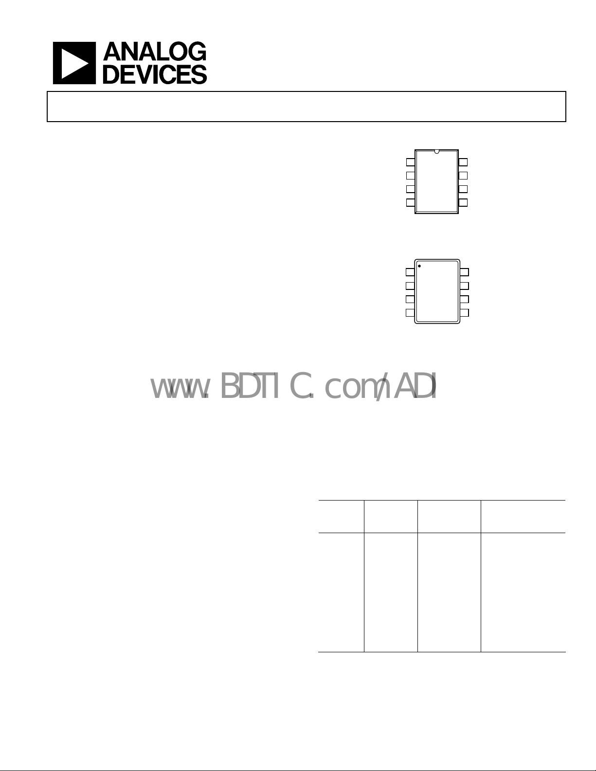
PIN CONFIGURATIONS
ADR440/
TP
1
ADR441/
ADR443/
V
2
IN
ADR444/
NC
3
ADR445
TOP VIEW
4
GND
(Not to Scale)
NOTES
1. NC = NO CONNECT
2. TP = TEST PIN (DO NOT CONNECT)
Figure 1. 8-Lead SOIC_N (R-Suffix)
ADR440/
1
TP
ADR441/
ADR443/
2
V
IN
ADR444/
NC
3
ADR445
GND
NOTES
1. NC = NO CONNECT
2. TP = TEST PIN (DO NOT CONNECT)
Figure 2. 8-Lead MSOP (RM-Suffix)
TOP VIEW
4
(Not to Scale)
TP
8
NC
7
6
V
OUT
5
TRIM
05428-001
8
TP
7
NC
V
6
OUT
TRIM
5
05428-002
GENERAL DESCRIPTION
The ADR44x series is a family of XFET® voltage references
featuring ultralow noise, high accuracy, and low temperature
drift performance. Using Analog Devices, Inc., patented
temperature drift curvature correction and XFET (eXtra
implanted junction FET) technology, voltage change vs.
temperature nonlinearity in the ADR44x is greatly minimized.
The XFET references offer better noise performance than
ried Zener references, and XFET references operate off
bu
low supply voltage headroom (0.5 V). This combination of
features makes the ADR44x family ideally suited for precision
signal conversion applications in high-end data acquisition
systems, optical networks, and medical applications.
The ADR44x family has the capability to source up to 10 mA of
o
utput current and sink up to −5 mA. It also comes with a trim
terminal to adjust the output voltage over a 0.5% range without
compromising performance.
Rev. C
Information furnished by Analog Devices is believed to be accurate and reliable. However, no
responsibility is assumed by Anal og Devices for its use, nor for any infringements of patents or ot her
rights of third parties that may result from its use. Specifications subject to change without notice. No
license is granted by implication or otherwise under any patent or patent rights of Analog Devices.
Trademarks and registered trademarks are the property of their respective owners.
Offered in two electrical grades, the ADR44x family is available in 8-lead MSOP and narrow SOIC packages. All versions
are specified over the extended industrial temperature range of
−40°C to +125°C.
Table 1. Selection Guide
Model
Output
oltage
V
(V)
Initial
Accuracy
(mV)
Temperature
Coefficient
(ppm/°C)
ADR440A 2.048 ±3 10
ADR440B 2.048 ±1 3
ADR441A 2.500 ±3 10
ADR441B 2.500 ±1 3
ADR443A 3.000 ±4 10
ADR443B 3.000 ±1.2 3
ADR444A 4.096 ±5 10
ADR444B 4.096 ±1.6 3
ADR445A 5.000 ±6 10
ADR445B 5.000 ±2 3
One Technology Way, P.O. Box 9106, Norwood, MA 02062-9106, U.S.A.
Tel: 781.329.4700 www.analog.com
Fax: 781.461.3113 ©2005–2008 Analog Devices, Inc. All rights reserved.

ADR440/ADR441/ADR443/ADR444/ADR445
www.BDTIC.com/ADI
TABLE OF CONTENTS
Features .............................................................................................. 1
Applications....................................................................................... 1
Pin Configurations ........................................................................... 1
General Description......................................................................... 1
Revision History ............................................................................... 2
Specifications..................................................................................... 3
ADR440 Electrical Characteristics............................................. 3
ADR441 Electrical Characteristics............................................. 4
ADR443 Electrical Characteristics............................................. 5
ADR444 Electrical Characteristics............................................. 6
ADR445 Electrical Characteristics............................................. 7
Absolute Maximum Ratings............................................................ 8
Thermal Resistance ...................................................................... 8
ESD Caution.................................................................................. 8
Typical Performance Characteristics ............................................. 9
Theory of Operation ...................................................................... 14
Power Dissipation Considerations ........................................... 14
Basic Voltage Reference Connections ..................................... 14
Noise Performance ..................................................................... 14
Tur n -O n Tim e ............................................................................ 14
Applications Information.............................................................. 15
Output Adjustment.................................................................... 15
Bipolar Outputs .......................................................................... 15
Negative Reference ..................................................................... 15
Programmable Voltage Source ................................................. 16
Programmable Current Source ................................................ 16
High Voltage Floating Current Source.................................... 16
Precision Output Regulator (Boosted Reference).................. 17
Outline Dimensions ....................................................................... 18
Ordering Guide .......................................................................... 19
REVISION HISTORY
3/08—Rev. B to Rev. C
Changes to Table 8............................................................................ 8
Change to Figure 11 ....................................................................... 10
Changes to Figure 36...................................................................... 15
Changes to Figure 39...................................................................... 16
Changes to Figure 41...................................................................... 17
Updated Outline Dimensions....................................................... 18
8/07—Rev. A to Rev. B
Change to Table 2, Ripple Rejection Ratio Specification ............ 3
Change to Table 3, Ripple Rejection Ratio Specification ............ 4
Change to Table 4, Ripple Rejection Ratio Specification ............ 5
Change to Table 5, Ripple Rejection Ratio Specification ............ 6
Change to Table 6, Ripple Rejection Ratio Specification ............ 7
9/06—Rev. 0 to Rev. A
Updated Format.................................................................. Universal
Changes to Features ..........................................................................1
Changes to Pin Configurations .......................................................1
Changes to Specifications Section...................................................3
Changes to Figure 4 and Figure 5....................................................9
Inserted Figure 6 and Figure 7.........................................................9
Changes to Figure 15...................................................................... 11
Changes to Power Dissipation Considerations Section ............ 14
Changes to Figure 35 and Figure 36............................................. 15
Changes to Figure 38 and Table 9................................................. 16
Updated Outline Dimensions....................................................... 18
Changes to Ordering Guide.......................................................... 19
10/05—Revision 0: Initial Version
Rev. C | Page 2 of 20
ADR440/ADR441/ADR443/ADR444/ADR445
www.BDTIC.com/ADI
SPECIFICATIONS
ADR440 ELECTRICAL CHARACTERISTICS
VIN = 3 V to 18 V, TA = 25°C, CIN = C
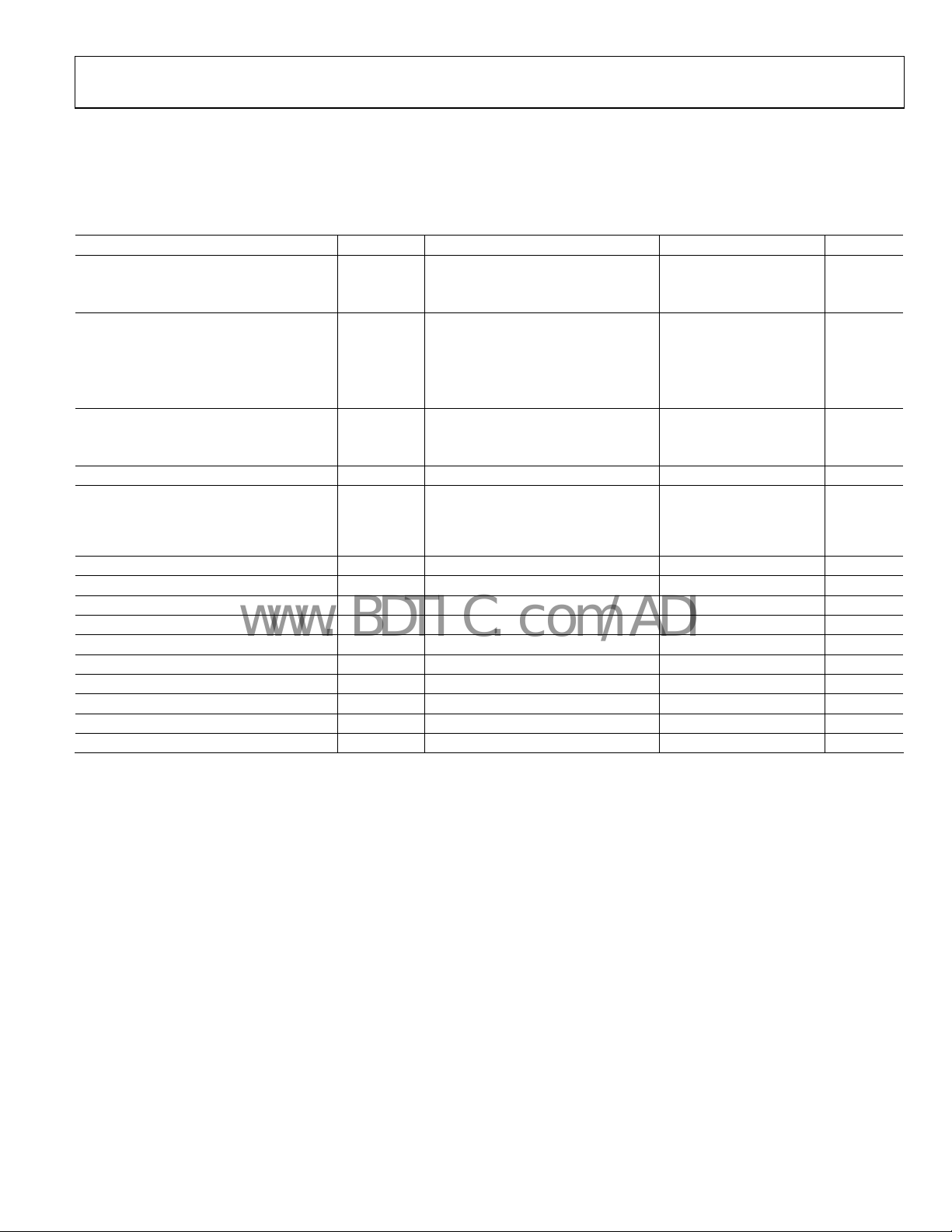
Table 2.
Parameter Symbol Conditions Min Typ Max Unit
OUTPUT VOLTAGE V
A Grade
B Grade
INITIAL ACCURACY V
A Grade
0.15 %
B Grade 1 mV
0.05 %
TEMPERATURE DRIFT TCV
A Grade −40°C < TA < +125°C 2 10 ppm/°C
B Grade −40°C < TA < +125°C 1 3 ppm/°C
LINE REGULATION ΔVO/ΔV
LOAD REGULATION ΔVO/ΔI
ΔVO/ΔI
QUIESCENT CURRENT I
VOLTAGE NOISE eN p-p 0.1 Hz to 10 Hz 1 μV p-p
VOLTAGE NOISE DENSITY e
TURN-ON SETTLING TIME t
LONG-TERM STABILITY
1
OUTPUT VOLTAGE HYSTERESIS V
RIPPLE REJECTION RATIO RRR fIN = 1 kHz −80 dB
SHORT CIRCUIT TO GND I
SUPPLY VOLTAGE OPERATING RANGE V
SUPPLY VOLTAGE HEADROOM VIN − V
1
The long-term stability specification is noncumulative. The drift in the subsequent 1000-hour period is significantly lower than in the first 1000-hour period.
= 0.1 µF, unless otherwise noted.
OUT
O
OERR
O
LOAD
2.045 2.048 2.051 V
2.047 2.048 2.049 V
3 mV
−40°C < TA < +125°C −20 +10 +20 ppm/V
IN
I
= 0 mA to 10 mA, VIN = 3.5 V,
LOAD
−40°C < T
I
LOAD
= 0 mA to −5 mA, VIN = 3.5 V,
LOAD
−40°C < T
IN
V
SC
N
R
O
O_HYS
IN
O
No load, −40°C < TA < +125°C 3 3.75 mA
1 kHz 45 nV/√Hz
10 μs
1000 hours 50 ppm
70 ppm
27 mA
3 18 V
500 mV
< +125°C
A
< +125°C
A
−50 +50 ppm/mA
−50 +50 ppm/mA
Rev. C | Page 3 of 20
ADR440/ADR441/ADR443/ADR444/ADR445
www.BDTIC.com/ADI
ADR441 ELECTRICAL CHARACTERISTICS
VIN = 3 V to 18 V, TA = 25°C, CIN = C
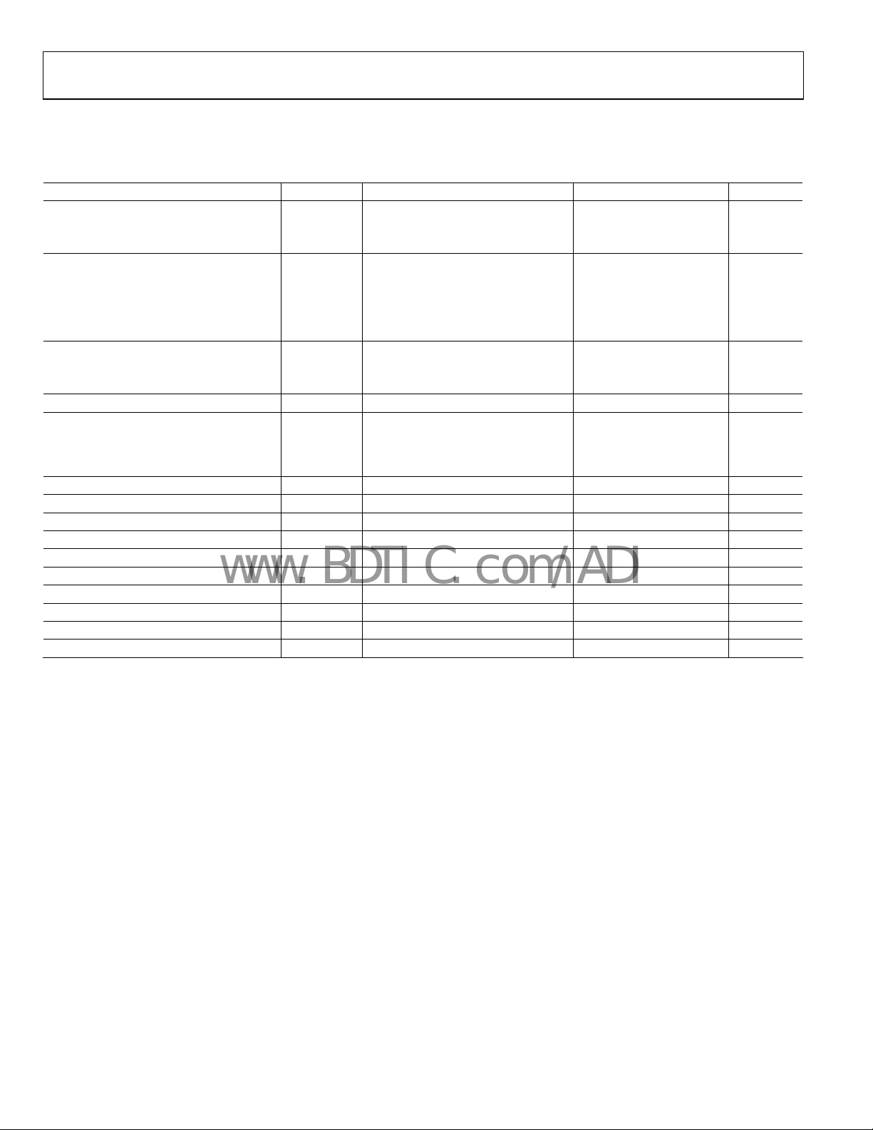
Table 3.
Parameter Symbol Conditions Min Typ Max Unit
OUTPUT VOLTAGE V
A Grade
B Grade
INITIAL ACCURACY V
A Grade
0.12 %
B Grade 1 mV
0.04 %
TEMPERATURE DRIFT TCV
A Grade −40°C < TA < +125°C 2 10 ppm/°C
B Grade −40°C < TA < +125°C 1 3 ppm/°C
LINE REGULATION ΔVO/ΔV
LOAD REGULATION ΔVO/ΔI
ΔVO/ΔI
QUIESCENT CURRENT I
VOLTAGE NOISE eN p-p 0.1 Hz to 10 Hz 1.2 μV p-p
VOLTAGE NOISE DENSITY e
TURN-ON SETTLING TIME t
LONG-TERM STABILITY
1
OUTPUT VOLTAGE HYSTERESIS V
RIPPLE REJECTION RATIO RRR fIN = 1 kHz −80 dB
SHORT CIRCUIT TO GND I
SUPPLY VOLTAGE OPERATING RANGE V
SUPPLY VOLTAGE HEADROOM VIN − V
1
The long-term stability specification is noncumulative. The drift in subsequent 1000-hour period is significantly lower than in the first 1000-hour period.
= 0.1 µF, unless otherwise noted.
OUT
O
OERR
O
LOAD
2.497 2.500 2.503 V
2.499 2.500 2.501 V
3 mV
−40°C < TA < +125°C 10 20 ppm/V
IN
I
= 0 mA to 10 mA, VIN = 4 V,
LOAD
−40°C < T
I
LOAD
= 0 mA to −5 mA, VIN = 4 V,
LOAD
−40°C < T
IN
V
SC
N
R
O
O_HYS
IN
O
No load, −40°C < TA < +125°C 3 3.75 mA
1 kHz 48 nV/√Hz
10 μs
1000 hours 50 ppm
70 ppm
27 mA
3 18 V
500 mV
< +125°C
A
< +125°C
A
−50 +50 ppm/mA
−50 +50 ppm/mA
Rev. C | Page 4 of 20
ADR440/ADR441/ADR443/ADR444/ADR445
www.BDTIC.com/ADI
ADR443 ELECTRICAL CHARACTERISTICS
VIN = 3.5 V to 18 V, TA = 25°C, CIN = C
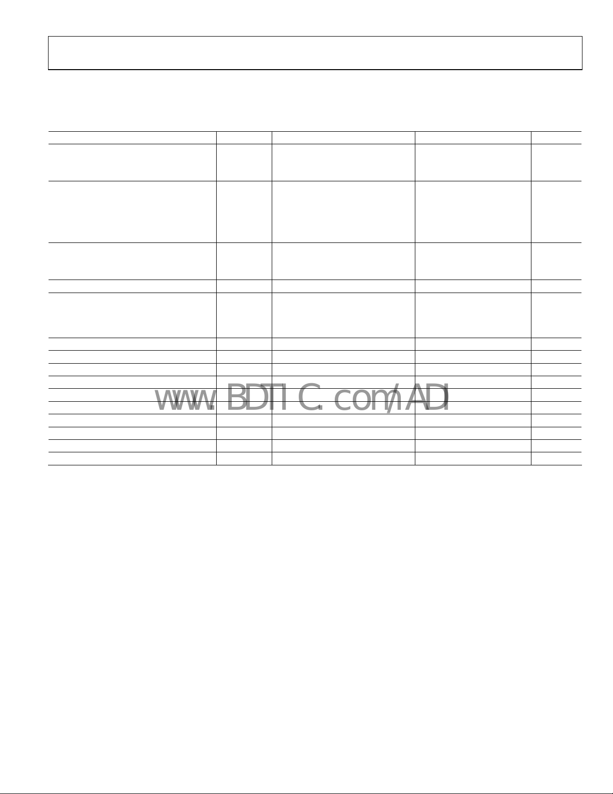
Table 4.
Parameter Symbol Conditions Min Typ Max Unit
OUTPUT VOLTAGE V
A Grade
B Grade
INITIAL ACCURACY V
A Grade
0.13 %
B Grade 1.2 mV
0.04 %
TEMPERATURE DRIFT TCV
A Grade −40°C < TA < +125°C 2 10 ppm/°C
B Grade −40°C < TA < +125°C 1 3 ppm/°C
LINE REGULATION ΔVO/ΔV
LOAD REGULATION ΔVO/ΔI
ΔVO/ΔI
QUIESCENT CURRENT I
VOLTAGE NOISE eN p-p 0.1 Hz to 10 Hz 1.4 μV p-p
VOLTAGE NOISE DENSITY e
TURN-ON SETTLING TIME t
LONG-TERM STABILITY
1
OUTPUT VOLTAGE HYSTERESIS V
RIPPLE REJECTION RATIO RRR fIN = 1 kHz −80 dB
SHORT CIRCUIT TO GND I
SUPPLY VOLTAGE OPERATING RANGE V
SUPPLY VOLTAGE HEADROOM VIN − V
1
The long-term stability specification is noncumulative. The drift in the subsequent 1000-hour period is significantly lower than in the first 1000-hour period.
= 0.1 µF, unless otherwise noted.
OUT
O
OERR
O
LOAD
2.996 3.000 3.004 V
2.9988 3.000 3.0012 V
4 mV
−40°C < TA < +125°C 10 20 ppm/V
IN
I
= 0 mA to 10 mA, VIN = 5 V,
LOAD
−40°C < T
I
LOAD
= 0 mA to −5 mA, VIN = 5 V,
LOAD
−40°C < T
IN
V
SC
N
R
O
O_HYS
IN
O
No load, −40°C < TA < +125°C 3 3.75 mA
1 kHz 57.6 nV/√Hz
10 μs
1000 hours 50 ppm
70 ppm
27 mA
3.5 18 V
500 mV
< +125°C
A
< +125°C
A
−50 +50 ppm/mA
−50 +50 ppm/mA
Rev. C | Page 5 of 20
ADR440/ADR441/ADR443/ADR444/ADR445
www.BDTIC.com/ADI
ADR444 ELECTRICAL CHARACTERISTICS
VIN = 4.6 V to 18 V, TA = 25°C, CIN = C
Table 5.
Parameter Symbol Conditions Min Typ Max Unit
OUTPUT VOLTAGE V
A Grade
B Grade
INITIAL ACCURACY V
A Grade
0.13 %
B Grade 1.6 mV
0.04 %
TEMPERATURE DRIFT TCV
A Grade −40°C < TA < +125°C 2 10 ppm/°C
B Grade −40°C < TA < +125°C 1 3 ppm/°C
LINE REGULATION ΔVO/ΔV
LOAD REGULATION ΔVO/ΔI
ΔVO/ΔI
QUIESCENT CURRENT I
VOLTAGE NOISE eN p-p 0.1 Hz to 10 Hz 1.8 μV p-p
VOLTAGE NOISE DENSITY e
TURN-ON SETTLING TIME t
LONG-TERM STABILITY
1
OUTPUT VOLTAGE HYSTERESIS V
RIPPLE REJECTION RATIO RRR fIN = 1 kHz −80 dB
SHORT CIRCUIT TO GND I
SUPPLY VOLTAGE OPERATING RANGE V
SUPPLY VOLTAGE HEADROOM VIN − V
1
The long-term stability specification is noncumulative. The drift in the subsequent 1000-hour period is significantly lower than in the first 1000-hour period.
= 0.1 µF, unless otherwise noted.
OUT
O
OERR
O
4.091 4.096 4.101 V
4.0944 4.096 4.0976 V
5 mV
−40°C < TA < +125°C 10 20 ppm/V
IN
I
LOAD
= 0 mA to 10 mA, VIN = 5.5 V,
LOAD
−40°C < T
I
LOAD
= 0 mA to −5 mA, VIN = 5.5 V,
LOAD
−40°C < T
IN
V
SC
N
R
O
O_HYS
IN
O
No load, −40°C < TA < +125°C 3 3.75 mA
1 kHz 78.6 nV/√Hz
10 μs
1000 hours 50 ppm
70 ppm
27 mA
4.6 18 V
500 mV
< +125°C
A
< +125°C
A
−50 +50 ppm/mA
−50 +50 ppm/mA
Rev. C | Page 6 of 20
 Loading...