

Precision Low-Drift 2.048 V/2.500 V
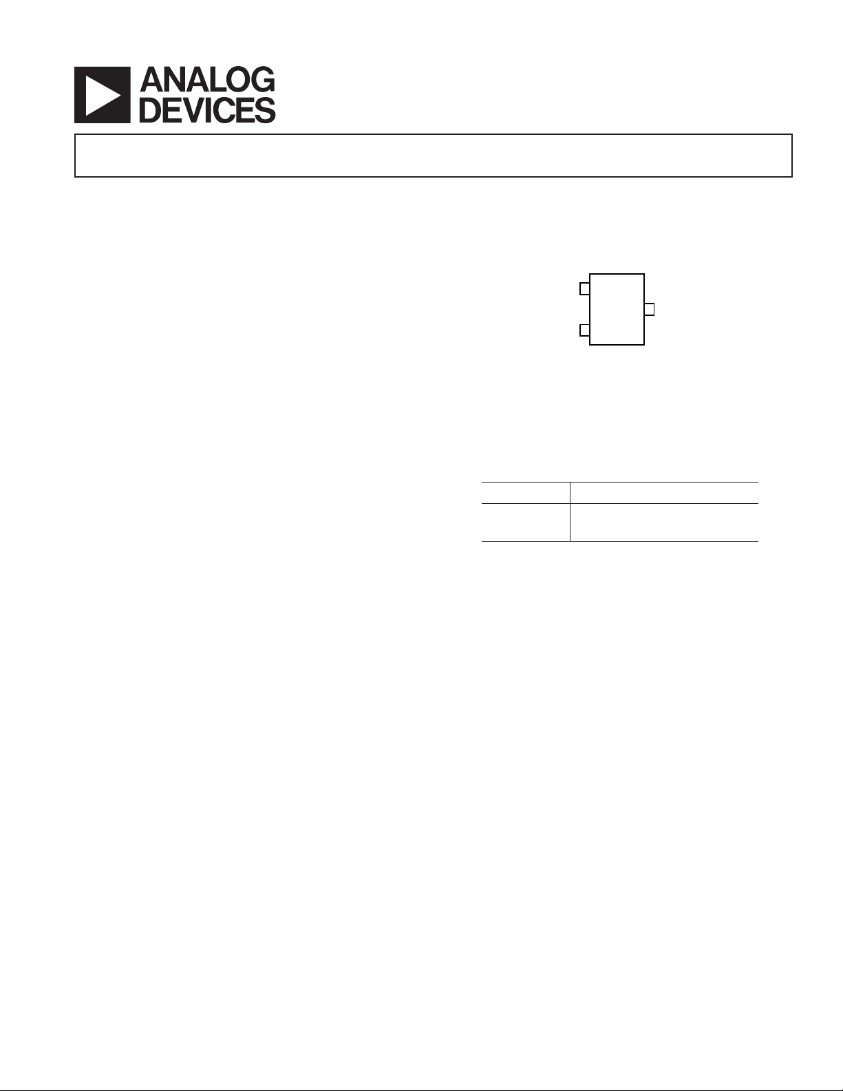
1
2
ADR380/
ADR381
(Not to Scale)
3
V
IN
GND
V
OUT
SOT-23 Voltage Reference
ADR380/ADR381
FEATURES
Initial Accuracy: ⴞ5 mV/ⴞ6 mV max
Initial Accuracy Error: ⴞ0.24%/ⴞ0.24%
Low TCV
: 25 ppm/ⴗC max
O
Load Regulation: 70 ppm/mA
Line Regulation: 25 ppm/V
Wide Operating Range:
2.4 V to 18 V for ADR380
2.8 V to 18 V for ADR381
Low Power: 120 A max
High Output Current: 5 mA
Wide Temperature Range: –40ⴗC to +85ⴗC
Tiny 3-Lead SOT-23 Package with Standard Pinout
APPLICATIONS
Battery-Powered Instrumentation
Portable Medical Instruments
Data Acquisition Systems
Industrial Process Control Systems
Hard Disk Drives
Automotive
GENERAL DESCRIPTION
The ADR380 and ADR381 are precision 2.048 V and 2.500 V
band gap voltage references featuring high accuracy, high stability, and low-power consumption in a tiny footprint. Patented
temperature drift curvature correction techniques minimize
nonlinearity of the voltage change with temperature. The wide
operating range and low power consumption make them ideal
for 3 V to 5 V battery-powered applications.
The ADR380 and ADR381 are micropower, low dropout
voltage (LDV) devices that provide a stable output voltage from
supplies as low as 300 mV above the output voltage. They are
specified over the industrial (–40°C to +85°C) temperature
range. ADR380/ADR381 is available in the tiny 3-lead SOT-23
package.
PIN CONFIGURATION
3-Lead SOT-23
(RT Suffix)
Table I. ADR38x Products
Part Number Nominal Output Voltage (V)
ADR380 2.048
ADR381 2.500
REV. A
Information furnished by Analog Devices is believed to be accurate and
reliable. However, no responsibility is assumed by Analog Devices for its
use, nor for any infringements of patents or other rights of third parties that
may result from its use. No license is granted by implication or otherwise
under any patent or patent rights of Analog Devices. Trademarks and
registered trademarks are the property of their respective owners.
One Technology Way, P.O. Box 9106, Norwood, MA 02062-9106, U.S.A.
Tel: 781/329-4700 www.analog.com
Fax: 781/326-8703 © 2004 Analog Devices, Inc. All rights reserved.

ADR380/ADR381–SPECIFICATIONS
ADR380 ELECTRICAL CHARACTERISTICS
(@ VIN = 5.0 V, TA = 25ⴗC unless otherwise noted.)
Parameter Symbol Conditions Min Typ Max Unit
Output Voltage V
Initial Accuracy Error V
O
OERR
2.043 2.048 2.053 V
–5 +5 mV
–0.24 +0.24 %
Temperature Coefficient TCV
O
–40°C < TA < +85°C525ppm/°C
0°C < TA< 70°C321ppm/°C
Minimum Supply Voltage Headroom V
Line Regulation ⌬V
IN
– V
/DV
O
O
IL ≤ 3 mA 300 mV
VIN = 2.5 V to 15 V 10 25 ppm/V
IN
–40°C < TA < +85°C
Load Regulation ⌬V
Quiescent Current I
Voltage Noise e
Turn-On Settling Time t
Long-Term Stability ⌬V
Output Voltage Hysteresis V
O
IN
N
R
O
O_HYS
/DI
LOADVIN
Ripple Rejection Ratio RRR f
Short Circuit to GND I
Specifications subject to change without notice.
SC
ADR380 ELECTRICAL CHARACTERISTICS
= 3 V, I
–40°C < T
= 0 mA to 5 mA 70 ppm/mA
LOAD
< +85°C
A
No Load 100 120 µA
–40°C < T
< +85°C 140 µA
A
0.1 Hz to 10 Hz 5 µV p-p
20 µs
1,000 Hrs 50 ppm
40 ppm
= 60 Hz 85 dB
IN
25 mA
(@ VIN = 15.0 V, TA = 25ⴗC unless otherwise noted.)
Parameter Symbol Conditions Min Typ Max Unit
Output Voltage V
Initial Accuracy Error V
O
OERR
2.043 2.048 2.053 V
–5 +5 mV
–0.24 +0.24 %
Temperature Coefficient TCV
Minimum Supply Voltage Headroom V
Line Regulation ⌬V
Load Regulation ⌬V
Quiescent Current I
Voltage Noise e
Turn-On Settling Time t
Long-Term Stability ⌬V
Output Voltage Hysteresis V
– V
IN
O
O
IN
N
R
O
O_HYS
O
O
/DV
/DI
Ripple Rejection Ratio RRR f
Short Circuit to GND I
Specifications subject to change without notice.
SC
–40°C < TA < +85°C525ppm/°C
0°C < T
< 70°C321ppm/°C
A
IL ≤ 3 mA 300 mV
VIN = 2.5 V to 15 V
IN
–40°C < T
LOADVIN
–40°C < T
= 3 V, I
< +85°C1025 ppm/V
A
= 0 mA to 5 mA
LOAD
< +85°C70ppm/mA
A
No Load 100 120 µA
–40°C < T
< +85°C 140 µA
A
0.1 Hz to 10 Hz 5 µV p-p
20 µs
1,000 Hrs 50 ppm
40 ppm
= 60 Hz 85 dB
IN
25 mA
REV. A–2–

SPECIFICATIONS
ADR380/ADR381
(continued)
ADR381 ELECTRICAL CHARACTERISTICS
(@ VIN = 5.0 V, TA = 25ⴗC unless otherwise noted.)
Parameter Symbol Conditions Min Typ Max Unit
Output Voltage V
Initial Accuracy Error V
O
OERR
2.494 2.5 2.506 V
–6 +6 mV
–0.24 +0.24 %
Temperature Coefficient TCV
O
–40°C < TA < +85°C525ppm/°C
0°C < TA < 70°C321ppm/°C
Minimum Supply Voltage Headroom V
Line Regulation ⌬V
IN
– V
/DV
O
O
IL ≤ 2 mA 300 mV
VIN = 2.8 V to 15 V 10 25 ppm/V
IN
–40°C < TA < +85°C
Load Regulation ⌬V
Quiescent Current I
Voltage Noise e
Turn-On Settling Time t
Long-Term Stability ⌬V
Output Voltage Hysteresis V
O
IN
N
R
O
O_HYS
/DI
LOADVIN
Ripple Rejection Ratio RRR f
Short Circuit to GND I
Specifications subject to change without notice.
SC
ADR381 ELECTRICAL CHARACTERISTICS
= 3.5 V, I
–40°C < T
A
= 0 mA to 5 mA 70 ppm/mA
LOAD
< +85°C
No Load 100 120 µA
–40°C < T
< +85°C 140 µA
A
0.1 Hz to 10 Hz 5 µV p-p
20 µs
1,000 Hrs 50 ppm
75 ppm
= 60 Hz 85 dB
IN
25 mA
(@ VIN = 15.0 V, TA = 25ⴗC unless otherwise noted.)
Parameter Symbol Conditions Min Typ Max Unit
Output Voltage V
Initial Accuracy Error V
O
OERR
2.494 2.5 2.506 V
–6 +6 mV
–0.24 +0.24 %
Temperature Coefficient TCV
Minimum Supply Voltage Headroom V
Line Regulation ⌬V
Load Regulation ⌬V
Quiescent Current I
Voltage Noise e
Turn-On Settling Time t
Long-Term Stability ⌬V
Output Voltage Hysteresis V
– V
IN
O
O
IN
N
R
O
O_HYS
O
O
/DV
/DI
Ripple Rejection Ratio RRR f
Short Circuit to GND I
Specifications subject to change without notice.
SC
–40°C < TA < +85°C525ppm/°C
0°C < T
< 70°C321ppm/°C
A
IL ≤ 2 mA 300 mV
VIN = 2.8 V to 15 V 10 25 ppm/V
IN
–40°C < T
LOADVIN
–40°C < T
= 3.5 V, I
< +85°C
A
LOAD
< +85°C
A
= 0 mA to 5 mA 70 ppm/mA
No Load 100 120 µA
–40°C < T
< +85°C 140 µA
A
0.1 Hz to 10 Hz 5 µV p-p
20 µs
1,000 Hrs 50 ppm
75 ppm
= 60 Hz 85 dB
IN
25 mA
REV. A –3–
ADR380/ADR381
1
2
ADR380/
ADR381
(Not to Scale)
3
V
IN
GND
V
OUT
ABSOLUTE MAXIMUM RATINGS
1
PIN CONFIGURATION
Supply Voltage . . . . . . . . . . . . . . . . . . . . . . . . . . . . . . . . . .18 V
Output Short-Circuit Duration to GND
> 15 V . . . . . . . . . . . . . . . . . . . . . . . . . . . . . . . . . 10 sec
V
IN
≤ 15 V . . . . . . . . . . . . . . . . . . . . . . . . . . . . . . Indefinite
V
IN
3-Lead SOT-23
(RT Suffix)
Storage Temperature Range
RT Package . . . . . . . . . . . . . . . . . . . . . . . . –65°C to +150°C
Operating Temperature Range
ADR380/ADR381 . . . . . . . . . . . . . . . . . . . . –40°C to +85°C
Junction Temperature Range
RT Package . . . . . . . . . . . . . . . . . . . . . . . . –65°C to +150°C
Lead Temperature Range (Soldering, 60 Sec) . . . . . . . . 300°C
Package Type
2
JA
JC
Unit
3-Lead SOT-23 (RT) 333 — °C/W
NOTES
1
Absolute maximum ratings apply at 25°C, unless otherwise noted.
2
θJA is specified for the worst-case conditions, i.e., θJA is specified for device
soldered in circuit board for surface-mount packages.
ORDERING GUIDE
Temperature Package Package Output Number of
Model Range Description Option Branding Voltage Parts per Reel
ADR380ART-R2 –40°C to +85°C SOT-23 RT-3 R2A 2.048 250
ADR380ART-REEL7 –40°C to +85°C SOT-23 RT-3 R2A 2.048 3,000
ADR380ARTZ-REEL7* –40°C to +85°C SOT-23 RT-3 R2A 2.048 3,000
ADR381ART-R2 –40°C to +85°C SOT-23 RT-3 R3A 2.500 250
ADR381ART-REEL7 –40°C to +85°C SOT-23 RT-3 R3A 2.500 3,000
ADR381ARTZ-REEL7* –40°C to +85°C SOT-23 RT-3 R3A 2.500 3,000
*Z = Pb-free part
CAUTION
ESD (electrostatic discharge) sensitive device. Electrostatic charges as high as 4,000 V readily
accumulate on the human body and test equipment and can discharge without detection. Although the
ADR380/ADR381 features proprietary ESD protection circuitry, permanent damage may occur on
devices subjected to high energy electrostatic discharges. Therefore, proper ESD precautions are
recommended to avoid performance degradation or loss of functionality.
REV. A–4–

ADR380/ADR381
PARAMETER DEFINITIONS
Temperature Coefficient
The change of output voltage over the operating temperature
change and normalized by the output voltage at 25°C, expressed
in ppm/°C. The equation follows:
TCV ppm C
O
°
/
[]
=
VCTT
VT VT
O
–
() ()
21
OO
°
25
()
–
×
()
21
6
10
×
where:
V
(25°C) = VO at 25°C.
O
V
) = VO at Temperature 1.
O (T1
V
) = VO at Temperature 2.
O (T2
Line Regulation
The change in output voltage due to a specified change in input
voltage. It includes the effects of self-heating. Line regulation is
expressed in either percent per volt, parts-per-million per volt,
or microvolts per volt change in input voltage.
Load Regulation
The change in output voltage due to a specified change in load
current. It includes the effects of self-heating. Load regulation is
expressed in either microvolts per milliampere, parts-permillion per milliampere, or ohms of dc output resistance.
Long-Term Stability
A typical shift in output voltage over 1,000 hours at a controlled
temperature. The graphs TPC 24 and TPC 25 show a sample
of parts measured at different intervals in a controlled environment of 50°C for 1,000 hours.
∆∆VVt–Vt
=
() ()
V ppm
[]
O
OO O
01
Vt–Vt
() ()
OO
01
=
Vt
()
O
0
6
×
10
where:
V
) = VO at Time 0.
O (t0
V
) = VO after 1,000 hours’ operation at a controlled
O (t1
temperature.
Note that 50°C was chosen since most applications we have
experienced run at a higher temperature than 25°C.
Thermal Hysteresis
The change of output voltage after the device is cycled through
temperature from +25°C to –40°C to +85°C and back to +25°C.
This is a typical value from a sample of parts put through
such a cycle.
VVCV
O_HYS O O_TC
V ppm
[]
O_HYS
25
=°
VCV
O O_TC
=
–
()
°
25
–
()
25
VC
°
()
O
6
10
×
where:
V
(25°C) = VO at 25°C.
O
V
= VO at 25°C after temperature cycle at +25°C to –40°C
O_TC
to +85°C and back to +25°C.
Typical Performance Characteristics
2.054
2.052
2.050
(V)
2.048
OUT
V
2.046
2.044
2.042
–40
–15 10 35 60 85
TEMPERATURE (ⴗC)
TPC 1. ADR380 Output Voltage vs. Temperature
REV. A
SAMPLE 1
SAMPLE 2
SAMPLE 3
–5–
2.506
2.504
(V)
OUT
V
2.502
2.500
2.498
2.496
2.494
–40
SAMPLE 1
SAMPLE 2
SAMPLE 3
–15 10 35 60 85
TEMPERATURE(ⴗC)
TPC 2. ADR381 Output Voltage vs. Temperature

ADR380/ADR381
30
TEMPERATURE +25ⴗC –40ⴗC +85ⴗC +25ⴗC
25
20
15
FREQUENCY
10
5
0
–11 –9 –7 –5 –3 –113
PPM (ⴗC)
TOTAL NUMBER
OF DEVICES = 130
5791113 15 17 19
TPC 3. ADR380 Output Voltage Temperature Coefficient
60
TEMPERATURE +25ⴗC
50
40
30
FREQUENCY
20
10
–40ⴗC +85ⴗC +25ⴗC
TOTAL NUMBER
OF DEVICES IN
SAMPLE = 450
140
120
100
80
60
40
SUPPLY CURRENT (A)
20
0
+85ⴗC
2.5 5.0 7.5 10.0 12.5 15.0
+25ⴗC
–40ⴗC
INPUT VOLTAGE (V)
TPC 6. ADR381 Supply Current vs. Input Voltage
70
IL = 0mA TO 5mA
60
50
40
30
VIN = 5V
20
LOAD REGULATION (ppm/mA)
10
VIN = 3V
0
–11 –9 –7 –5 –3 –1 1 3
PPM (ⴗC)
579111315–15 –13
TPC 4. ADR381 Output Voltage Temperature Coefficient
140
120
100
80
60
40
SUPPLY CURRENT (A)
20
+85ⴗC
0
2.5 5.0 7.5 10.0 12.5
+25ⴗC
–40ⴗC
15.0
INPUT VOLTAGE (V)
TPC 5. ADR380 Supply Current vs. Input Voltage
0
–40 –15 10 35 60
TEMPERATURE (ⴗC)
85
TPC 7. ADR380 Load Regulation vs. Temperature
70
IL = 5mA
60
50
40
30
20
LOAD REGULATION (ppm/mA)
10
0
–40 –15 10 35 60
VIN = 3.5V
VIN = 5V
TEMPERATURE (ⴗC)
85
TPC 8. ADR381 Load Regulation vs. Temperature
REV. A–6–

ADR380/ADR381
(mA)
V
OUT
DEVIATION (ppm)
–260
0
FREQUENCY
10
20
30
40
50
60
–200
–140
–80 –20
40 100
160 220 340 400
280
TEMPERATURE +25ⴗC –40ⴗC 85ⴗC +25ⴗC
5
VIN = 2.5V TO 15V
4
3
2
LINE REGULATION (ppm/V)
1
0
–40 –15 10 35 60
TEMPERATURE (ⴗC)
85
TPC 9. ADR380 Line Regulation vs. Temperature
5
VIN = 2.8V TO 15V
4
3
0.8
0.6
0.4
0.2
DIFFERENTIAL VOLTAGE (V)
–40ⴗC
0
012 345
LOAD CURRENT
+85ⴗC
+25ⴗC
TPC 12. ADR381 Minimum Input/Output Voltage
Differential vs. Load Current
2
LINE REGULATION (ppm/V)
1
0
–40 –15 10 35 60 85
TPC 10. ADR381 Line Regulation vs. Temperature
0.8
0.6
0.4
0.2
DIFFERENTIAL VOLTAGE (V)
0
012 34
TPC 11. ADR380 Minimum Input/Output
Voltage Differential vs. Load Current
–40ⴗC
TEMPERATURE (ⴗC)
LOAD CURRENT (mA)
+85ⴗC
+25ⴗC
TPC 13. ADR381 V
2V/DIV
5
TIME (1s/DIV)
Hysteresis
OUT
TPC 14. ADR381 Typical Noise Voltage 0.1 Hz to 10 Hz
REV. A
–7–

ADR380/ADR381
)
100V/DIV
LOAD OFF
CL = 0F
V
OUT
V
LOAD
LOAD = 1mA
ON
1V/DIV
2V/DIV
TIME (10ms/DIV
TPC 15. ADR381 Typical Noise Voltage 10 Hz to 10 kHz
C
= 0F
BYPASS
V
0.5V/DIV
LINE INTERRUPTION
TIME (10s/DIV)
OUT
V
IN
1V/DIV
0.5V/DIV
TPC 16. ADR381 Line Transient Response
C
= 0.1F
BYPASS
TIME (200s/DIV)
TPC 18. ADR381 Load Transient Response with
C
= 0 µF
L
CL = 1nF
V
LOAD OFF
TIME (200s/DIV)
OUT
V
LOAD
LOAD = 1mA
1V/DIV
ON
2V/DIV
TPC 19. ADR381 Load Transient Response with
CL = 1 nF
CL = 100nF
V
0.5V/DIV
OUT
LINE INTERRUPTION
TIME (10s/DIV)
1V/DIV
0.5V/DIV
TPC 17. ADR381 Line Transient Response
V
LOAD OFF
TIME (200s/DIV)
OUT
V
LOAD
LOAD = 1mA
ON
1V/DIV
2V/DIV
TPC 20. ADR381 Load Transient Response with
= 100 nF
C
L
REV. A–8–

TIME (200s/DIV)
HOURS
0
–150
0
100
DRIFT (ppm)
–100
–50
50
100
150
200 300 400
500
600 700 800 900
1000
CONDITIONS: VIN = 6V IN A CONTROLLED
ENVIRONMENT 50ⴗC ⴞ1ⴗC
HOURS
0
–150
0
100
DRIFT (ppm)
–100
–50
50
100
150
200 300 400
500
600 700 800 900
1000
CONDITIONS: VIN = 6V IN A CONTROLLED
ENVIRONMENT 50ⴗC ⴞ1ⴗC
RL = 500⍀
V
OUT
V
IN
ADR380/ADR381
2V/DIV
5V/DIV
TPC 21. ADR381 Turn-On/Turn-Off Response at 5 V
CB = 0.1F
CL = 40pF
(10⍀/DIV)
OUT
Z
10
100
CL = 1F
1k 10k 100k
FREQUENCY (Hz)
CL = 0.1F
1M
TPC 22. ADR381 Output Impedance vs. Frequency
TPC 23. ADR380 Long-Term Drift
TPC 24. ADR381 Long-Term Drift
REV. A
–9–
ADR380/ADR381
THEORY OF OPERATION
Band gap references are the high performance solution for low
supply voltage and low power voltage reference applications,
and the ADR380/ADR381 are no exception. But the uniqueness of this product lies in its architecture. By observing Figure
1, the ideal zero TC band gap voltage is referenced to the
output, not to ground. The band gap cell consists of the PNP
pair Q51 and Q52, running at unequal current densities. The
difference in V
results in a voltage with a positive TC which is
BE
amplified up by the ratio of 2 × R58/R54. This PTAT voltage,
combined with V
of Q51 and Q52, produce the stable band
BEs
gap voltage. Reduction in the band gap curvature is performed
by the ratio of the two resistors R44 and R59. Precision laser
trimming and other patented circuit techniques are used to
further enhance the drift performance.
V
R49
R48
IN
V
OUT
GND
Q1
R59
R54
R53
+
Q51
–
R60
R44
R58
Q52
R61
Figure 1. Simplified Schematic
Device Power Dissipation Considerations
The ADR380/ADR381 are capable of delivering load currents
to 5 mA with an input voltage that ranges from 2.8 V (ADR381
only) to 15 V. When this device is used in applications with
large input voltages, care should be taken to avoid exceeding the
specified maximum power dissipation or junction temperature
that could result in premature device failure. The following
formula should be used to calculate a device’s maximum junction temperature or dissipation:
–
TT
J
P
=
D
A
θ
J
A
where:
is the device power dissipation,
P
D
T
and TA are junction and ambient temperatures,
J
respectively, and
is the device package thermal resistance.
θ
J
A
Input Capacitor
Input capacitor is not required on the ADR380/ADR381. There
is no limit for the value of the capacitor used on the input, but a
capacitor on the input will improve transient response in applications where the load current suddenly increases.
Output Capacitor
The ADR380/ADR381 do not need an output capacitor for
stability under any load condition. An output capacitor, typically
0.1 µF, will take out any very low level noise voltage, and will
not affect the operation of the part. The only parameter that will
degrade by putting an output capacitor here is turn-on time.
(This will vary depending on the size of the capacitor.) Load
transient response is also improved with an output capacitor. A
capacitor will act as a source of stored energy for a sudden increase in load current.
APPLICATIONS
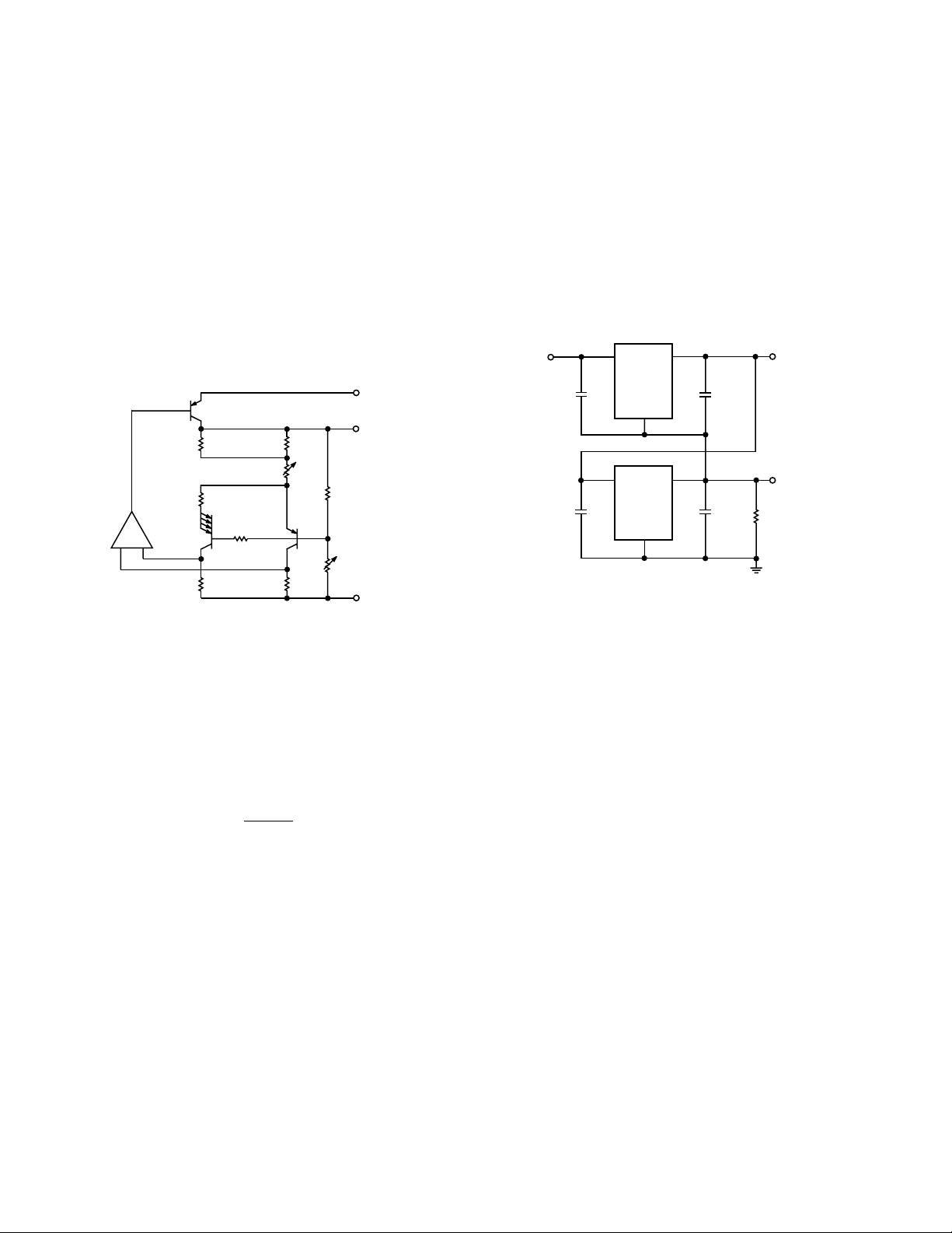
Stacking Reference ICs for Arbitrary Outputs
Some applications may require two reference voltage sources
which are a combined sum of standard outputs. The following
circuit shows how this stacked output reference can be implemented:
U2
GND
3
U1
GND
3
2
V
OUT
C2
1F
2
V
OUT
C4
1F
R1
3.9k⍀
V
V
OUT2
OUT1
1
V
IN
C1
0.1F
C3
0.1F
V
ADR380/
1
V
IN
ADR381
IN
ADR380/
ADR381
Figure 2. Stacking Voltage References with the
ADR380/ADR381
Two ADR380s or ADR381s are used; the outputs of the individual references are simply cascaded to reduce the supply
current. Such configuration provides two output voltages—
and V
V
OUT1
V
is the sum of this voltage and the terminal voltage of U2.
OUT2
OUT2
. V
is the terminal voltage of U1, while
OUT1
U1 and U2 can be chosen for the two different voltages that
supply the required outputs.
While this concept is simple, a precaution is in order. Since the
lower reference circuit must sink a small bias current from U2,
plus the base current from the series PNP output transistor in
U2, the external load of either U1 or R1 must provide a path for
this current. If the U1 minimum load is not well-defined, the
resistor R1 should be used, set to a value that will conservatively
pass 600 µA of current with the applicable V
across it. Note
OUT1
that the two U1 and U2 reference circuits are locally treated as
macrocells, each having its own bypasses at input and output for
optimum stability. Both U1 and U2 in this circuit can source dc
currents up to their full rating. The minimum input voltage, V
is determined by the sum of the outputs, V
OUT2
, plus the
,
S
300 mV dropout voltage of U2.
A Negative Precision Reference Without Precision Resistors
In many current-output CMOS DAC applications where the
output signal voltage must be of the same polarity as the reference voltage, it is often required to reconfigure a current-switching
DAC into a voltage-switching DAC through the use of a 1.25 V
reference, an op amp, and a pair of resistors. Using a currentswitching DAC directly requires an additional operational
amplifier at the output to reinvert the signal. A negative voltage
REV. A–10–

ADR380/ADR381
GND
V
OUT
V
IN
U1
ADR380/
ADR381
3
V
O
2
R2
100⍀
1
C1
0.001F
Q1
2N7002
+8 –15V
R1
100k⍀
R
L
V
IN
A1
–V
+V
AD820
reference is then desirable from the point that an additional
operational amplifier is not required for either reinversion
(current-switching mode) or amplification (voltage-switching
mode) of the DAC output voltage. In general, any positive
voltage reference can be converted into a negative voltage reference through the use of an operational amplifier and a pair of
matched resistors in an inverting configuration. The disadvantage to this approach is that the largest single source of error in
the circuit is the relative matching of the resistors used.
The circuit in Figure 3 avoids the need for tightly matched
resistors with the use of an active integrator circuit. In this circuit,
the output of the voltage reference provides the input drive for
the integrator. The integrator, to maintain circuit equilibrium,
adjusts its output to establish the proper relationship between
the reference’s V
and GND. Thus, any negative output
OUT
voltage desired can be chosen by simply substituting for the
appropriate reference IC. A precaution should be noted with
this approach: although rail-to-rail output amplifiers work best
in the application, these operational amplifiers require a finite
amount (mV) of headroom when required to provide any load
current. The choice for the circuit’s negative supply should take
this issue into account.
R4
IN
U1
GND
3
2
V
OUT
100k⍀
1
V
IN
C1
1F
0.1F
V
C2
ADR380
1k⍀
R3
C3
1F
C4
1F
+5V
R5
U2
OP195
100⍀
–V
REF
+V
A1
–V
–5V
1
V
IN
C1
0.1F
1F
V
IN
C2
ADR380
U1
GND
3
2
V
OUT
C3
1F
ADJUST
R1
P1
I
SY
I
OUT
R
L
Figure 4. A Precision Current Source
Precision High Current Voltage Source
In some cases, the user may want higher output current delivered
to a load and still achieve better than 0.5% accuracy out of the
ADR380/ADR381. The accuracy for a reference is normally
specified on the data sheet with no load. However, the output
voltage changes with load current.
The circuit in Figure 5 provides high current without compromising the accuracy of the ADR380/ADR381. By op amp action,
V
follows V
O
with very low drop in R1. To maintain circuit
REF
equilibrium, the op amp also drives the N-Ch MOSFET Q1 into
saturation to maintain the current needed at different loads. R2
is optional to prevent oscillation at Q1. In such an approach, hundreds of milliamps of load current can be achieved and the current
is limited by the thermal limitation of Q1. V
= VO + 300 mV.
IN
Figure 3. A Negative Precision Voltage Reference
Uses No Precision Resistors
Precision Current Source
Many times in low power applications, the need arises for a precision current source that can operate on low supply voltages.
As shown in Figure 4, the ADR380/ADR381 can be configured
as a precision current source. The circuit configuration illustrated
is a floating current source with a grounded load. The reference’s
output voltage is bootstrapped across R
(R1 + P1), which sets
SET
Figure 5. ADR380/ADR381 for Precision High
Current Voltage Source
the output current into the load. With this configuration, circuit
precision is maintained for load currents in the range from the
reference’s supply current, typically 90 µA to approximately 5 mA.
REV. A
–11–

ADR380/ADR381
OUTLINE DIMENSIONS
3-Lead Small Outline Transistor Package [SOT-23-3]
(RT-3)
Dimensions shown in millimeters
3.04
2.90
1.40
1.30
1.20
PIN 1
0.10
0.01
2.80
3
1
1.90 BSC
SEATING
PLANE
COMPLIANT TO JEDEC STANDARDS TO-236AB
2
0.95 BSC
2.64
2.10
0.50
0.30
1.12
0.89
0.60
0.50
0.40
0.20
0.08
Tape and Reel Dimensions
Dimensions shown in millimeters
C02175–0–7/04(A)
4.10
4.00
3.20
3.10
2.90
3.90
1.55
1.50
1.50
8.30
8.00
7.70
DIRECTION OF UNREELING
Revision History
2.05
2.00
1.95
1.00 MIN
1.85
1.75
1.65
3.55
3.50
3.45
0.75 MIN
1.10
1.00
0.90
2.80
2.70
2.60
0.35
0.30
0.25
7" REEL 100.00
13" REEL 330.00
20.20
MIN
OR
1.50 MIN
13.20
13.00
12.80
14.40 MAX
7" REEL 50.00 MIN
OR
13" REEL 100.00 MIN
9.90
8.40
8.40
Location Page
7/04—Data Sheet Changed from Rev. 0 to Rev. A.
Updated format . . . . . . . . . . . . . . . . . . . . . . . . . . . . . . . . . . . . . . . . . . . . . . . . . . . . . . . . . . . . . . . . . . . . . . . . . . . . . . . . . . .Universal
Changes to ORDERING GUIDE . . . . . . . . . . . . . . . . . . . . . . . . . . . . . . . . . . . . . . . . . . . . . . . . . . . . . . . . . . . . . . . . . . . . . . . . . . . 4
Updated OUTLINE DIMENSIONS . . . . . . . . . . . . . . . . . . . . . . . . . . . . . . . . . . . . . . . . . . . . . . . . . . . . . . . . . . . . . . . . . . . . . . . 12
–12–
REV. A
 Loading...