Analog Devices ADM9690 Datasheet

Power Supply and Watchdog Timer
a
FEATURES
Precision Voltage Monitor (4.31 V)
Watchdog Timeout Monitor
Selectable Watchdog Timeout—0.75 ms, 1.5 ms,
12.5 ms, 25 ms
Two RESET Outputs
APPLICATIONS
Microprocessor Systems
Computers
Printers
Controllers
Intelligent Instruments
GENERAL DESCRIPTION
The ADM9690 contains a voltage monitoring comparator and a
watchdog timer monitor. It is designed to monitor the 5 V
power supply to a microprocessor and the microprocessor operation via a watchdog function.
The voltage monitoring comparator monitors the voltage on
V
. If it drops outside tolerance, as will happen during a
MON
power-fail, two reset signals are generated. Both reset signals go
active (low) simultaneously. They will remain active while
is below the threshold, and for 50 ms (RESET(1)) or
V
MON
60 ms (RESET(2)) after V
old. RESET(1) is intended to provide a power-on reset signal
for the µP while RESET(2) is used to hold additional circuitry
in a reset state until the µP has regained control following a
power-up. The voltage monitoring circuitry remains operational
with V
as low as 2 V.
CC
climbs above the reset thresh-
MON
Monitoring Circuit
ADM9690
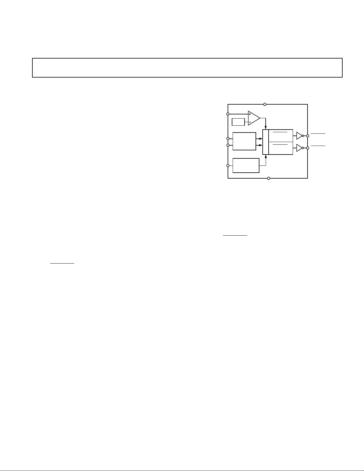
FUNCTIONAL BLOCK DIAGRAM
V
CC
V
MON
4.31V
OSC SEL1
OSC SEL2
WATCHDOG
INPUT (WDI)
WATCHDOG
TIMEBASE
WATCHDOG
TRANSITION
DETECTOR
The watchdog timer monitoring circuit is designed to monitor
the activity on the WDI input. This input is normally connected
to an output line on the µP. Its function is to check that the
microprocessor has not stalled in an infinite loop. If there is a
period of inactivity for the watchdog timeout period, both reset
outputs are activated. As above, RESET(1) remains low for
50 ms while RESET(2) remains low for an additional 10 ms.
The watchdog timer is restarted when RESET(1) goes inactive.
The actual watchdog timeout period is adjustable using two
select inputs SEL1 and SEL2.
The ADM9690 is available in an 8-lead SOIC package. It is
specified over the industrial temperature range.
GND
ADM9690
RESET(1)
TIMER
RESET(2)
TIMER
RESET(1)
RESET(2)
REV. A
Information furnished by Analog Devices is believed to be accurate and
reliable. However, no responsibility is assumed by Analog Devices for its
use, nor for any infringements of patents or other rights of third parties
which may result from its use. No license is granted by implication or
otherwise under any patent or patent rights of Analog Devices.
One Technology Way, P.O. Box 9106, Norwood, MA 02062-9106, U.S.A.
Tel: 781/329-4700 World Wide Web Site: http://www.analog.com
Fax: 781/326-8703 © Analog Devices, Inc., 2000

ADM9690–SPECIFICATIONS
(VCC = Full Operating Range. TA = T
MIN
to T
unless otherwise noted)
MAX
Parameter Min Typ Max Units Test Conditions/Comments
VCC OPERATING VOLTAGE RANGE 4.3 5.5 V
SUPPLY CURRENT 55 100 µA
RESET AND WATCHDOG TIMER
Reset Voltage Threshold 4.2 4.31 4.42 V V
Falling TA = 0°C to +70°C
MON
Reset Threshold Hysteresis 30 mV
Reset Timeout Delay (t1) 50 75 ms Figure 7, 8
RESET(2) Timeout Delay (t2) 10 15 ms Figure 7, 8
WATCHDOG TIMEOUT PERIOD (TWD) 0.4 0.75 1.28 ms SEL2 = 0, SEL1 = 0
1.0 1.5 2.4 ms SEL2 = 0, SEL1 = 1
9.0 12.5 19 ms SEL2 = 1, SEL1 = 0
18 25 38 ms SEL2 = 1, SEL1 = 1
WDI INPUT PULSEWIDTH 100 ns V
RESET(1)/(2) Output Voltage 0.1 0.4 V I
0.3 0.4 V I
0.45 0.7 V I
3.5 V I
= 0.4, VIH = 3.5 V
IL
= 3.2 mA
SINK
= 10 mA,
SINK
= 15 mA,
SINK
SOURCE
WDI INPUT THRESHOLD
Logic Low 0.8 V 150 ns Pulse
Logic High 3.5 V 150 ns Pulse
WDI Input Current 1.2 5 µA WDI = V
–5 –1.2 µA WDI = 0 V
SEL1/2 Input Current –1 +1 µA SEL = V
–10 –5 10 µA SEL = 0 V
Specifications subject to change without notice.
= 1 µA
CC
CC
–2–
REV. A
 Loading...