Charge Pump Driver for LCD
Preliminary Technical Data
FEATURES
ADM8846 drives 6 LEDs from a 2.6 V to 5.5 V (li-ion) input
supply
1x/1.5x/2x Fractional Charge Pump to maximise power
efficiency
1% Max LED Current Matching
Up to 88% Power Efficiency over Li-ion Range
Powers Main and Sub Display LEDs with individual
shutdown
Package footprint only 9mm
Package height only 0.9mm
Low power shutdown mode
Shutdown Function
Soft-start limiting inrush current
APPLICATIONS
Mobile phones with Main and Sub Displays
White LED Backlighting
Camera Flash/Strobes and Movie Light Applications
Micro TFT color displays
DSC
PDA’s
2
(3mm x 3mm)
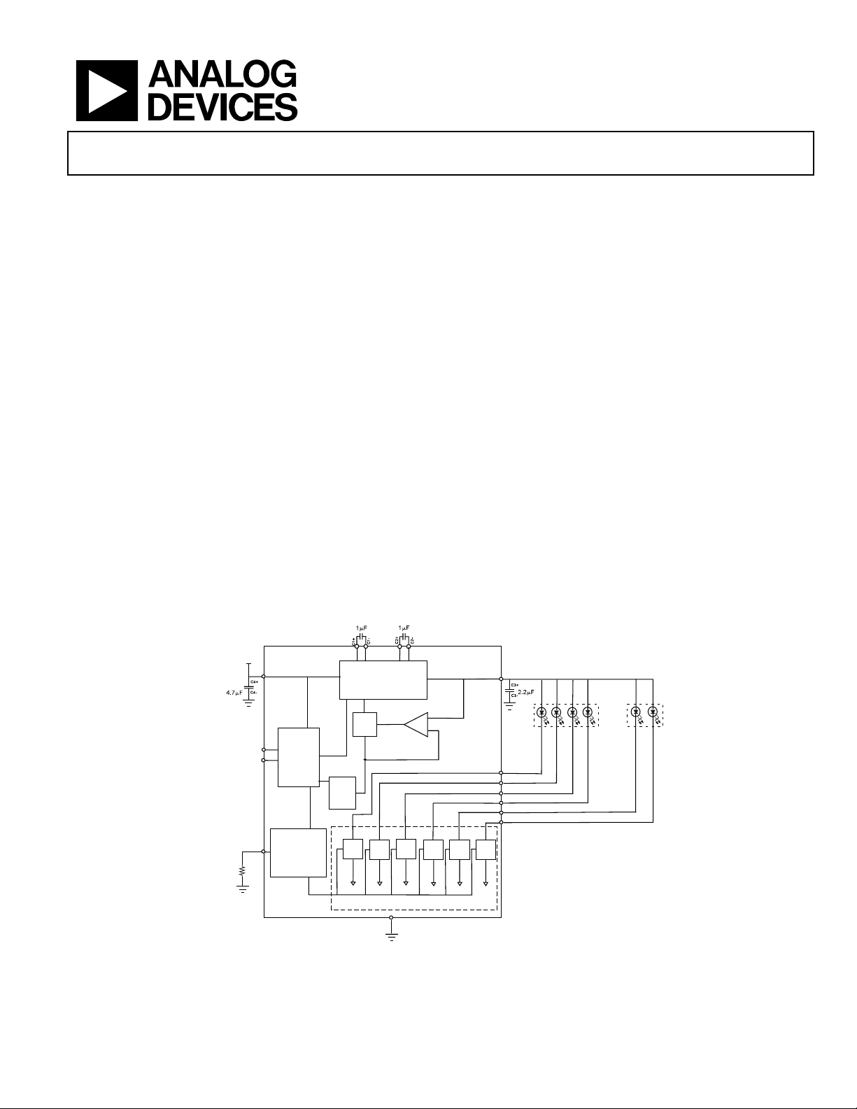
FUNCTIONAL BLOCK DIAGRAM
C1 C2
White LED Backlights
ADM8846
GENERAL DESCRIPTION
The ADM8846 provides the power required to drive up to six
LEDs, using charge pump technology. The LEDs are used for
backlighting a color LCD display, with up to four LEDs in the
main display and up to two LEDs in the sub display, with
regulated constant current for uniform brightness intensity.
Two digital input control pins, CTRL1 and CTRL2 control the
shutdown operation and the brightness of the main and sub
displays.
To maximize power efficiency, a charge pump that can operate
in either of a 1x, 1.5x or 2x mode is used. The charge pump
automatically switches between 1x/1.5x/2x modes based on the
input voltage, to maintain sufficient drive for the LED anodes at
the highest power efficiency.
Improved brightness matching of the LEDs is achieved by the
use of a feedback pin to sense individual LED current with a
maximum matching accuracy of 1%.
VCC
Rset
C4
CTRL1
CTRL2
Iset
ADM8846
Control
Logic
LED Current
Control
Circuit
Charge Pump
1x/1.5x/2x mode
Osc
Vref
Current
Current
Control
Control
2
1
Current Controlled Sinks
Current
Control
GND
3
Figure 1. ADM8846 FUNCTIONAL BLOCK DIAGRAM
Rev. PrA_06/04
Information furnished by Analog Devices is believed to be accurate and reliable.
However, no responsibility is assumed by Analog Devices for its use, nor for any
infringements of patents or other rights of third parties that may result from its use.
Specifications subject to change without notice. No license is granted by implication
or otherwise under any patent or patent rights of Analog Devices. Trademarks and
registered trademarks are the property of their respective companies.
+
-
Current
Control
Vout
C3
MAIN
FB1
FB2
FB3
FB4
FB5
FB6
Current
Current
Control
Control
5
4
6
SUB
One Technology Way, P.O. Box 9106, Norwood, MA 02062-9106, U.S.A.
Tel: 781.329.4700
Fax: 781.326.8703 © 2004 Analog Devices, Inc. All rights reserved.
www.analog.com

ADM8846 Preliminary Technical Data
TABLE OF CONTENTS
General Description..................................................................... 1
ADM8846—Specifications...............................................................3
Thermal Characteristics .............................................................. 3
Absolute Maximum Ratings.............................................................4
ESD Caution.................................................................................. 4
Pin Configuration and Function Description ...............................5
Typical Performance Characteristics ..............................................6
ADM8846 Operation ..................................................................... 10
Output Current Capability........................................................ 11
Automatic Gain Control............................................................ 11
Current Matching....................................................................... 11
ADM8846 Brightness Control With a Digital PWM Signal..... 12
REVISION HISTORY
REV. PrA 06/04
ADM8846 LED Brightness Control Using a PWM Signal
Applied to V
ADM8846 LED Brightness Control Using a DC Voltage
Applied to V
ADM8846 Applications ..................................................................15
Layout considerations and noise .............................................. 15
White LED Shorting .................................................................. 15
Driving Fewer than six LEDs.................................................... 15
Driving Flash LEDs.................................................................... 15
Driving Camera Light, Main and sub leds.............................. 16
ADM8846 Power Efficiency...........................................................17
Outline Dimensions........................................................................18
Ordering Guide .......................................................................... 18
.......................................................................... 14
PWM
....................................................................... 14
BRIGHT
Rev. PrA 06/04 | Page 2 of 18

Preliminary Technical Data ADM8846
ADM8846—SPECIFICATIONS
(VCC = +2.6V TO 5.5V; T
Table 1.
PARAMETER Min Typ Max Units Test Conditions
Input Voltage,VCC 2.6 5.5 V
Supply Current,ICC 2.6 4 m A All 6 LEDs Disabled, Vcc = 3.3V, R
CTRL1 = 1, CRTL2 = 1
Shutdown Current 5 uA TA= 25°C
Charge-Pump Frequency 1.5 M H z
Charge Pump Mode Thresholds
1.5x to 2x 3.33 V
Accuracy 4 %
2x to 1.5x 3.36 V
Accuracy 4 %
Hysteresis 40 m V
1x to 1.5x 4.77 V
Accuracy 4 %
1.5x to 1x 4.81 V
Accuracy 4 %
Hysteresis 40 m V
Iset Pin
LED : LED Matching -1 +1 % I
LED : I
Accuracy -1 +1 %
SET
Iset pin voltage 1.18 V
I
to I
LED
Ratio 120
SET
Min Compliance on FB pin 0.2 0.3 V I
Charge Pump Output Resistance 1.2 1.7 Ohm 1x Mode
3.5 4.5 Ohm 1.5x Mode
8.0 11 Ohm 2x Mode
LED Current 30 m A See Note 1 and Figure 22
PWM 0.1 200 KHz
Digital Inputs
Input Hi 1.6 V
Input Low 0.4 V
Input Leakage Current 1 uA
Charge Pump Power Efficiency 88 % CTRL1 = 1, CRTL2 = 1, Vcc = 3.4V, V
I
Vout Ripple 30 m V Vcc = 3.6V, I
THERMAL CHARACTERISTICS
16-Lead LFCSP Package:
θ
= 50°C/Watt
JA
= -40°C to 85°C unless otherwise noted; C1,C2 = 1.0µF; C3 = 2.2µF; C4 = 4.7µF)
A
= 20mA, VFB =0.4V
LED
= 20mA, R
I
LED
= 7.08K, VFB =0.4V, Vcc = 3.6V, TA = 25°C,
SET
Note 2
= 20mA
SET
2.6V ≤ Vcc ≤ 4.2V
2.6V ≤ Vcc ≤ 4.2V
= 20mA
FB
= 20mA, All 6 LEDs Enabled
LED
= 7.08kOhm
SET
= 0.2V,
FB
Rev. PrA 06/04| Page 3 of 18

ADM8846 Preliminary Technical Data
ABSOLUTE MAXIMUM RATINGS
Table 2. (TA = 25°C unless otherwise noted)
Parameter Rating
Supply Voltage VCC –0.3 V to +6.0 V
I
–0.3 V to +2.0 V
SET
CTRL1, CTRL2 –0.3 V to +6.0 V
V
shorted (Note 3) Indefinite
OUT
Feedback pins FB1 to FB6 –0.3 V to +6.0 V
Operating Temperature Range –40°C to +85°C
V
(Note 4) 180mA
OUT
Storage Temperature Range –65°C to +125°C
Power Dissipation 2mW
ESD Class 1
Note 1: LED Current should be derated above T
> 65C, refer to
A
Figure 22.
Note 2: Guaranteed by design. Not 100% production tested.
Note 3: Short through LED.
Note 4: Based on long term current density limitations.
Stresses above those listed under Absolute Maximum Ratings
may cause permanent damage to the device. This is a stress
rating only; functional operation of the device at these or any
other conditions above those indicated in the operational
section of this specification is not implied. Exposure to absolute
maximum rating conditions for extended periods may affect
device reliability.
ESD CAUTION
ESD (electrostatic discharge) sensitive device. Electrostatic charges as high as 4000 V readily accumulate on the
human body and test equipment and can discharge without detection. Although this product features
proprietary ESD protection circuitry, permanent damage may occur on devices subjected to high energy
electrostatic discharges. Therefore, proper ESD precautions are recommended to avoid performance
degradation or loss of functionality.
Main Display
Sub Display
Vcc
2.6V- 5.5V
VOUT
ADM8846
CTRL1
CTRL2
I
SET
R
SET
GND
FB1
FB2
FB3
FB4
FB5
FB6
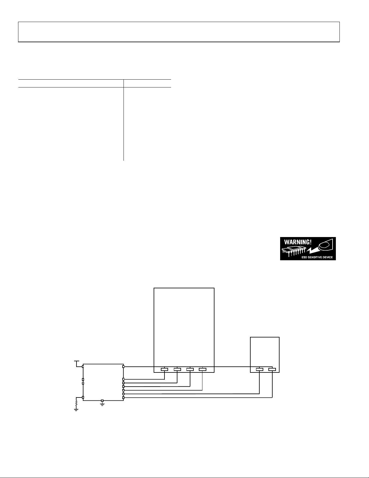
Figure 2. ADM8846 Typical Application Diagram
Rev. PrA 06/04 | Page 4 of 18

Preliminary Technical Data ADM8846
PIN CONFIGURATION AND FUNCTION DESCRIPTION
Table 3.
Pin
ADM8846
1 VOUT
2 C2+ Flying Capacitor 2 Positive Connection
3 I
4 FB1
5 FB2
6 FB3
7 FB4
8 FB5
9 FB6
10 G N D Device Ground Pin.
11 C2− Flying Capacitor 2 Negative Connection.
12 CTRL2
13 CTRL1
14 C1− Flying Capacitor 1 Negative Connection.
15 Vcc
16 C1+ Flying Capacitor 1 Positive Connection.
- EP Expose Paddle. Connect the exposed paddle to GND.
Mnemonic Function
Charge Pump Output. A 2.2µF capacitor to ground is required on this pin. Connect Vout to the anodes
of all the LEDs.
SET
Bias current set input. The current flowing through the R
I
curent. Connect a resistor R
LED
LED1 Cathode connection and Charge Pump Feedback. The current flowing in LED1 is 120 times the
current flowing through R
LED2 Cathode connection and Charge Pump Feedback. The current flowing in LED2 is 120 times the
current flowing through R
LED3 Cathode connection and Charge Pump Feedback. The current flowing in LED3 is 120 times the
current flowing through R
LED4 Cathode connection and Charge Pump Feedback. The current flowing in LED4 is 120 times the
current flowing through R
LED5 Cathode connection and Charge Pump Feedback. The current flowing in LED5 is 120 times the
current flowing through R
LED6 Cathode connection and Charge Pump Feedback. The current flowing in LED6 is 120 times the
current flowing through R
Digital Input. 3 V CMOS Logic. Used with CTRL1 to control the shutdown operation of the main and sub
LEDs.
Digital Input. 3 V CMOS Logic. Used with CTRL2 to control the shutdown operation of the main and sub
LEDs.
Positive Supply Voltage Input. Connect this pin to a 2.6 V to 5.5 V supply with a 4.7µF decoupling
capacitor.
resistor I
to GND to set the bias current as V
SET
, I
.
SET
SET
, I
. When using fewer than six LEDs this pin can be left unconnected.
SET
SET
, I
. When using fewer than six LEDs this pin can be left unconnected.
SET
SET
, I
. When using fewer than six LEDs this pin can be left unconnected.
SET
SET
, I
. When using fewer than six LEDs this pin can be left unconnected.
SET
SET
, I
. When using fewer than six LEDs this pin can be left unconnected.
SET
SET
SET
is gained up by 120 to give the
SET
. (Note: Vset = 1.18V)
SET/RSET
16
15
14
13
ISET
FB1
1
2
3
(NOT TO SCALE)
4
ADM8846
TOP VIEW
56
7
12
CTRL2
11
10
GND
9
FB6
8
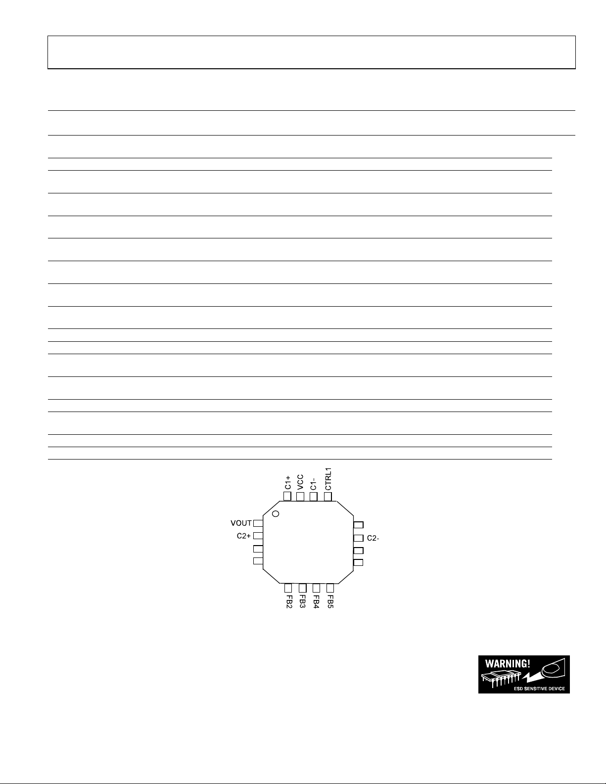
Figure 3. ADM8846 Pin Configuration
ESD (electrostatic discharge) sensitive device. Electrostatic charges as high as 4000 V readily accumulate on the
human body and test equipment and can discharge without detection. Although this product features
proprietary ESD protection circuitry, permanent damage may occur on devices subjected to high energy
electrostatic discharges. Therefore, proper ESD precautions are recommended to avoid performance
degradation or loss of functionality.
Rev. PrA 06/04| Page 5 of 18

ADM8846 Preliminary Technical Data
TYPICAL PERFORMANCE CHARACTERISTICS
35
30
25
20
15
LED Curr en t (mA)
10
5
4.75 6.75 8.75 10.75 12.75 14.75
Rset (koh m)
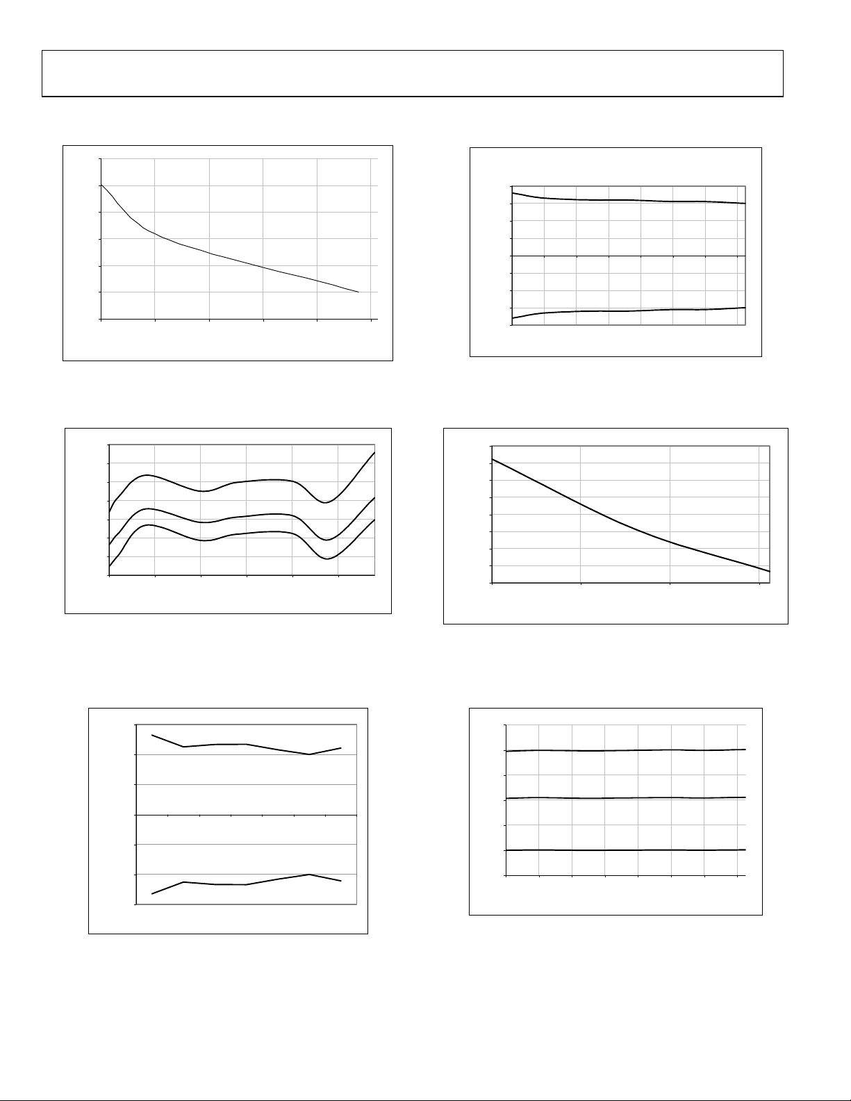
Figure 4. LED Current vs. R
20.35
20.3
20.25
20.2
20.15
LED current (mA)
20.1
20.05
20
2.6 3.1 3.6 4.1 4.6 5.1
-40'C
25'C
85'C
Supply Voltage (V)
Resistor
SET
Figure 6. LED Current (mA) vs. Temperature (°C), 6 LEDs enabled.
0.4
0.3
0.2
0.1
0
2.6 3 3.4 3.8 4.2 4.6 5 5.4
-0.1
Matching Error (%)
-0.2
-0.3
-0.4
Max Positive Match ing Error
Max Negative Matching Error
Supply Voltage (V)
Figure 5. LED Current Matching Error (%) vs. Supply Voltage (V),
= 25°C and I
T
A
20.24
20.22
20.2
20.18
20.16
20.14
LED Current (mA)
20.12
20.1
20.08
-40 0 40 80
Figure 7. I
(mA) Variation over Temperature (°C), with Vcc = 3.6V
LED
= 20mA
LED
Temperature ('C)
Figure 8. I
0.300
0.200
0.100
0.000
-40-200 25456585
% Error
-0.100
-0.200
-0.300
Matching (%) over Temperature (°C), with Vcc = 3.6,
LED
= 20mA , 6 LEDs enabled.
I
LED
Temperature
Rev. PrA 06/04 | Page 6 of 18
35
30
25
20
15
LED Current (mA)
10
5
2.6 3 3.4 3.8 4.2 4.6 5 5.4
Supply Voltage (V)
Figure 9. LED Current (mA) vs. Supply Voltage (V)
 Loading...