

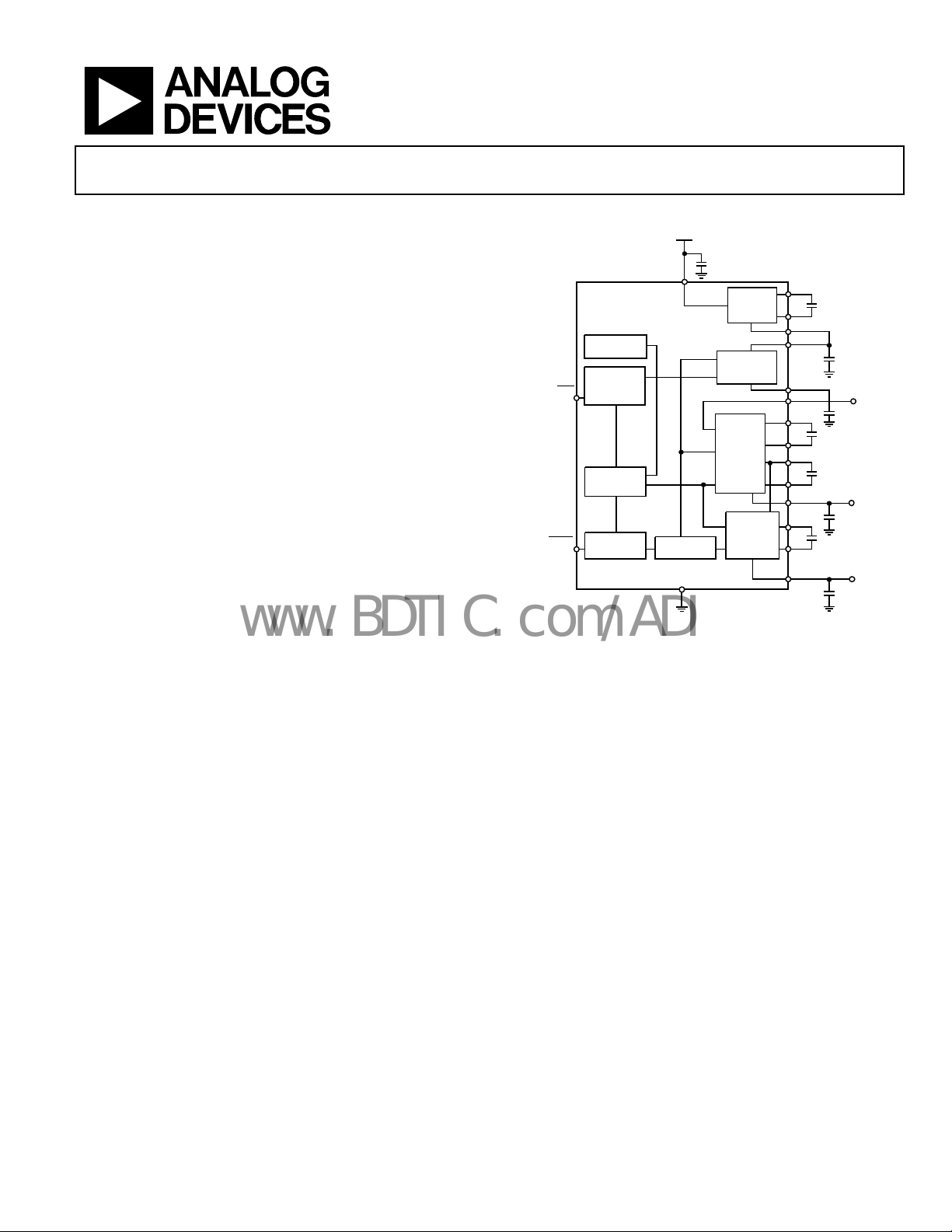
Charge Pump Regulator
www.BDTIC.com/ADI
FEATURES
3 voltages (+5 V, +15 V, −15 V) from a single 3 V supply
Power efficiency optimized for use with TFT in mobile
phones
Low quiescent current
Low shutdown current (<5 μA)
Shutdown function
Option to use external LDO
APPLICATIONS
Hand-held instruments
TFT LCD panels
Cellular phones
LDO_ON/OFF
SHDN
for Color TFT Panels
ADM8839
FUNCTIONAL BLOCK DIAGRAM
C5, 2.2µF
V
ADM8839
OSCILLATOR
CONTROL
LOGIC
TIMING
GENERATOR
SHUTDOWN
CONTROL
CC
DISCHARGE
GND
Figure 1.
VOLTAGE
DOUBLER
LDO
VOLTAGE
REGULATOR
DOUBLE
VOLTAGE
TRIPLER
TRIPLE
VOLTAGE
INVERTER
C1+
C1–
VOUT
LDO_IN
+5VOUT
+5VIN
C2+
C2–
C3+
C3–
+15VOUT
C4+
C4–
–15VOUT
C1, 2.2µF
C6, 2.2µF
C7, 2.2µF
C2, 0.22µF
C3, 0.22µF
C8, 0.22µF
C4, 0.22µF
C9, 0.22µF
+5V
+15V
–15V
03075-001
GENERAL DESCRIPTION
The ADM8839 is a charge pump regulator used for color thin
film transistor (TFT) liquid crystal displays (LCDs). Using
charge pump technology, the device can be used to generate
three voltages (+5 V ± 2%, +15 V, −15 V) from a single 3 V
supply. These voltages are then used to provide supplies for the
LCD controller (5 V) and the gate drives for the transistors in
the panel (+15 V and −15 V). Only a few external capacitors are
needed for the charge pumps. An efficient low dropout (LDO)
voltage regulator ensures that the power efficiency is high, and
provides a low ripple 5 V output. This LDO can be shut down
and an external LDO can be used to regulate the 5 V doubler
output and drive the input to the charge pump section that
generates the +15 V and −15 V outputs, if required by the user.
The ADM8839 has a power save shutdown feature. The 5 V
o
utput consumes the most power, so power efficiency is also
maximized on this output with an oscillator-enabling scheme
(Green Idle™). This effectively senses the load current that is
flowing and turns on the charge pump only when charge needs
to be delivered to the 5 V pump doubler output.
The ADM8839 is fabricated using CMOS technology for
mini
mal power consumption. The part is packaged in a 20-lead
LFCSP (lead frame chip scale package).
Rev. C
Information furnished by Analog Devices is believed to be accurate and reliable. However, no
responsibility is assumed by Anal og Devices for its use, nor for any infringements of patents or ot her
rights of third parties that may result from its use. Specifications subject to change without notice. No
license is granted by implication or otherwise under any patent or patent rights of Analog Devices.
Trademarks and registered trademarks are the property of their respective owners.
One Technology Way, P.O. Box 9106, Norwood, MA 02062-9106, U.S.A.
Tel: 781.329.4700 www.analog.com
Fax: 781.461.3113 ©2006 Analog Devices, Inc. All rights reserved.

ADM8839
www.BDTIC.com/ADI
TABLE OF CONTENTS
Features.............................................................................................. 1
ESD Caution...................................................................................4
Applications....................................................................................... 1
Functional Block Diagram .............................................................. 1
General Description ......................................................................... 1
Revision History ............................................................................... 2
Specifications..................................................................................... 3
Timing Specifications .................................................................. 3
Absolute Maximum Ratings............................................................ 4
Thermal Characteristics .............................................................. 4
REVISION HISTORY
7/06—Rev. B to Rev. C
Updated Format..................................................................Universal
Changes to Table 1............................................................................ 3
Changes to Table 5............................................................................ 5
Changes to Ordering Guide.......................................................... 10
Updated Outline Dimension......................................................... 10
Pin Configuration and Function Descriptions..............................5
Typical Performance Characteristics..............................................6
Theory of Operation .........................................................................8
Power Sequencing.........................................................................8
Transient Response .......................................................................8
Boosting the Current Drive of the ±15 V Supply .....................8
Outline Dimensions....................................................................... 10
Ordering Guide .......................................................................... 10
7/05—Rev. A to Rev. B
U
pdated Ordering Guide .................................................................3
2/03—Rev. 0 to Rev. A
C
hanged Specifications.....................................................................2
Updated Outline Dimensions..........................................................8
Rev. C | Page 2 of 12
ADM8839
www.BDTIC.com/ADI
SPECIFICATIONS
VCC = 3 V (+40%/−10%); TA = −40°C to +85°C; C1, C5, C6, C7 = 2.2 μF; C2, C3, C4, C8, C9 = 0.22 μF; unless otherwise noted.
Table 1.
Parameter Test Conditions Min Typ Max Unit
INPUT VOLTAGE, VCC 2.7 4.2 V
SUPPLY CURRENT, ICC Unloaded 250 500 μA
Shutdown mode, TA = 25°C 5 μA
+5 V OUTPUT
Output Voltage IL = 10 μA to 20 mA 4.9 5.0 5.1 V
Output Current 5 20 mA
Output Ripple 8 mA load 10 mV p-p
Transient Response IL stepped from 10 μA to 8 mA 5 μs
+15 V OUTPUT
Output Voltage IL = 1 μA to 150 μA 14.0 15.0 16.0 V
Output Current 1 150 μA
Output Ripple IL = 100 μA 50 mV p-p
−15 V OUTPUT
Output Voltage IL = −1 μA to −150 μA −16.0 −15.0 −14.0 V
Output Current −150 −1 μA
Output Ripple IL = −100 μA 50 mV p-p
POWER EFFICIENCY R5 V
CHARGE PUMP FREQUENCY 60 100 140 kHz
CONTROL PINS, SHDN
Input Voltage, V
SHDN
Digital Input Current ±1 μA
Digital Input Capacitance1 10 pF
LDO_ON/OFF
Input Voltage Low = External LDO 0.3 × VCC V
High = Internal LDO 0.7 × VCC V
Digital Input Current ±1 μA
Digital Input Capacitance1 10 pF
1
Guaranteed by design. Not 100% production tested.
load = 5 mA, ±15 V load = ±150 μA, VCC = 3.0 V 82 %
OUT
low = shutdown mode
SHDN
high = normal mode
SHDN
0.3 × V
0.7 × V
V
CC
V
CC
TIMING SPECIFICATIONS
VCC = 3 V, TA = 25°C; C1, C5, C6, C7 = 2.2 μF; C2, C3, C4, C8, C9 = 0.22 μF.
Table 2.
Parameter Test Conditions/Comments Min Typ Max Unit
POWER-UP SEQUENCE
+5 V Rise Time, t
+15 V Rise Time, t
−15 V Fall Time, t
Delay Between −15 V Fall and +15 V, t
10% to 90%, see Figure 14 250 μs
R5V
10% to 90%, see Figure 14 3 ms
R15V
90% to 10%, see Figure 14 3 ms
FM15V
See Figure 14 600 μs
DELAY
POWER-DOWN SEQUENCE
+5 V Fall Time, t
+15 V Fall Time, t
−15 V Rise Time, t
90% to 10%, see Figure 14 35 ms
F5V
90% to 10%, see Figure 14 10 ms
F15V
10% to 90%, see Figure 14 20 ms
RM15V
Rev. C | Page 3 of 12
ADM8839
www.BDTIC.com/ADI
ABSOLUTE MAXIMUM RATINGS
TA = 25°C, unless otherwise noted.
Table 3.
Parameter Rating
Supply Voltage −0.3 V to +6.0 V
Input Voltage on Digital Inputs −0.3 V to +6.0 V
Output Short-Circuit Duration to GND 10 sec
Output Voltage
+5 V Output 0 V to 7.0 V
–15 V Output −17 V to +0.3 V
+15 V Output −0.3 V to +17 V
Operating Temperature Range −40°C to +85°C
Power Dissipation 50 mW
Storage Temperature Range −65°C to +150°C
ESD Class I
Stresses above those listed under Absolute Maximum Ratings
ma
y cause permanent damage to the device. This is a stress
rating only; functional operation of the device at these or any
other conditions above those indicated in the operational
section of this specification is not implied. Exposure to absolute
maximum rating conditions for extended periods may affect
device reliability.
THERMAL CHARACTERISTICS
θJA is specified for the worst-case conditions, that is, a device
soldered in a circuit board for surface-mount packages.
Table 4. Thermal Resistance
Package Type θJA Unit
20-Lead LFCSP_VQ 31°C °C/W
ESD CAUTION
ESD (electrostatic discharge) sensitive device. Electrostatic charges as high as 4000 V readily accumulate on
the human body and test equipment and can discharge without detection. Although this product features
proprietary ESD protection circuitry, permanent damage may occur on devices subjected to high energy
electrostatic discharges. Therefore, proper ESD precautions are recommended to avoid performance
degradation or loss of functionality.
Rev. C | Page 4 of 12

ADM8839
www.BDTIC.com/ADI
PIN CONFIGURATION AND FUNCTION DESCRIPTIONS
17 –15VOUT
16 C4+
18 GND
19 C1–
20 C1+
VCC1
VOUT 2
LDO_IN3
+5VOUT 4
+5VIN 5
Figure 2. Pin Configuration
PIN 1
INDICATOR
ADM8839
TOP VIEW
SHDN 7
LDO_ON/OFF 6
15 C4–
14 C2+
13 C2–
12 C3+
11 C3–
8
CC
V
GND 9
+15VOUT 10
3075-002
Table 5. Pin Function Descriptions
Pin No. Mnemonic Description
1 VCC
Positive Supply Voltage Input. Connect this pin to the 3 V sup
ply with a 2.2 μF decoupling capacitor. Must be
electrically tied together with Pin 8 by a PCB trace.
2 VOUT
Voltage Doubler Output. This is deriv
ed by doubling the 3 V supply. A 2.2 μF capacitor to ground is required
on this pin.
3 LDO_IN
4 +5VOUT
Voltage Regulator Input. The user can bypass this cir
5 V Output. This is derived by doubling and r
egulating the 3 V supply. A 2.2 μF capacitor to ground is required
cuit by using the LDO_ON/OFF
pin.
on this pin to stabilize the regulator.
5 +5VIN 5 V Input. This is the input to the voltage tripler and inverter charge pump circuits.
6
LDO_ON/OFF
Control Logic Input. 3 V CMOS logic. A logic high selects the internal LDO for regulation of the 5 V voltage
doubler output. A logic low isolates the internal LDO from the rest of the charge pump circuits. This allows the
use of an external LDO to regulate the 5 V voltage doubler output. The output of this LDO is then fed back into
the voltage tripler and inverter circuits of the ADM8839.
7
Digital Input. 3 V CMOS logic. Active low shutdown control. This shuts down the timing generator and enables
SHDN
the discharge circuit to dissipate the charge on the voltage outputs, thus driving them to 0 V.
8 V
Connect this pin to VCC. Must be electrically tied with Pin 1 by a PCB trace.
CC
9 GND Connect this pin to GND. Must be electrically tied with Pin 18 by a PCB trace.
10 +15VOUT 15 V Output. This is derived by tripling the 5 V regulated output. A 0.22 μF capacitor is required on this pin.
11, 12 C3−, C3+ External Capacitor C3 is connected between these pins. A 0.22 μF capacitor is recommended.
13, 14 C2−, C2+ External Capacitor C2 is connected between these pins. A 0.22 μF capacitor is recommended.
15, 16 C4−, C4+ External Capacitor C4 is connected between these pins. A 0.22 μF capacitor is recommended.
17 −15VOUT
−15 V Output. This is derived by tripling and inverting the 5
V regulated output. A 0.22 μF capacitor is required
on this pin.
18 GND Device Ground. Must be electrically tied with Pin 9 by a PCB trace.
19, 20 C1−, C1+ External Capacitor C1 is connected between these pins. A 2.2 μF capacitor is recommended.
Rev. C | Page 5 of 12

ADM8839
www.BDTIC.com/ADI
TYPICAL PERFORMANCE CHARACTERISTICS
5.10
5.05
5.00
4.95
4.90
4.85
LDO O/P VOLTAGE (V)
4.80
4.75
4.70
DEVICE AT +25°C
DEVICE AT –40°C
3.1 9.35.37.2 2.9 3.3 3.7 4.1 4.2
SUPPLY VOLTAGE (V)
Figure 3. LDO O/P Voltage Variation over Temperature and Supply
DEVICE AT +85°C
03075-003
84
83
82
81
80
79
78
77
LDO POW ER E FFICIENCY (%)
76
75
387512 4 6
LOAD CURRENT (mA)
Figure 6. LDO Power Efficiency vs. Load Current, V
CC
= 3 V
03075-006
5.020
5.015
5.010
5.005
LDO O/P VOLTAGE (V)
5.000
4.995
20461357
I
(mA)
LOAD
8
03075-004
Figure 4. LDO O/P Voltage vs. Load Current
100
90
80
70
60
50
+15V/–15V POWER EFF ICIENCY (%)
40
30
30 001070501920 40 60 80
I
(µA)
LOAD
0
3075-005
400
350
300
250
SUPPLY CURRENT (µA)
200
150
3.1 9.35.37.2 2.9 3.3 3.7 4.1 4.2
SUPPLY VOLTAGE (V)
03075-007
Figure 7. Supply Current vs. Supply Voltage
15.1
15.0
14.9
14.8
14.7
14.6
14.5
14.4
OUTPUT VOLTAGE (V)
14.3
14.2
14.1
500 100 150 200
I
+15V AT 25°C
–15V AT 25°C
(µA)
LOAD
3075-008
Figure 5. +15 V/−15 V Power Efficiency vs. Load Current
Rev. C | Page 6 of 12
Figure 8. +15 V/−15 V Output Voltage vs. Load Current, Typical Configuration

ADM8839
www.BDTIC.com/ADI
+15V OUTPUT
5VOUT
–15V OUTPUT
Figure 9. +15 V and −15 V Outputs at Power-Up
V
RIPPLE (DOUBLER OUTPUT RIPPLE)
OUT
LDO OUTPUT RIPPLE
RIPPLE
V
CC
LOAD ENABLE
5V OUTPUT
03075-012
03075-009
Figure 12. Output Transient Response for Maximum Load Current
+15V OUTPUT
–15V OUTPUT
Figure 10. Output Ripple on LDO (5 V Output)
LOAD DISABLE
5V OUTPUT
Figure 11. 5 V Output Transient Response, Load Disconnected
5VOUT
03075-013
03075-010
Figure 13. +15 V and −15 V Outputs at Power-Down
03075-011
Rev. C | Page 7 of 12

ADM8839
www.BDTIC.com/ADI
THEORY OF OPERATION
POWER SEQUENCING
For the TFT panel to power up correctly, the gate drive supplies
must be sequenced such that the −15 V supply is up before the
+15 V supply. The ADM8839 controls this sequence. When the
device is turned on (a logic high on
allows the −15 V output to ramp immediately but holds off the
+15 V output. It continues to do this until the negative output
has reached −3 V. At this point, the positive output is enabled
and allowed to ramp to +15 V. This sequence is highlighted in
Figure 14.
SHDN
), the ADM8839
BOOSTING THE CURRENT DRIVE OF THE ±15 V SUPPLY
The ADM8839 ±15 V output can deliver 150 μA of current in
the typical configuration, as shown in Figure 15. It is also
ossible to draw 100 μA from the +15 V output and 200 μA
p
from the −15 V output, or vice versa. It is possible to draw a
maximum of only 300 μA combined from the +15 V and the
−15 V outputs at any time (see
+5V
OUT (Pin 4) is connected to +5VIN (Pin 5), as shown in
the functional block diagram (see
Figure 16). In this configuration,
Figure 1).
V
CC
SHDN
t
R5V
+5V
+15V
–15V
90%
10%
t
FM15V
10%
t
DELAY
90%
10%
90%
–3V
t
R15V
t
F5V
t
F15V
t
RM15V
Figure 14. Power Sequence
TRANSIENT RESPONSE
The ADM8839 features extremely fast transient response,
making it very suitable for fast image updates on TFT LCD
panels. This means that even under changing load conditions,
there is still very effective regulation of the 5 V output.
nd Figure 12 show how the 5 V output responds when a
a
imum load is dynamically connected and disconnected.
max
Note that the output settles within 5 μs to less than 1% of the
output level.
Figure 11
C5, 2.2µF
V
CC
ADM8839
OSCILLATOR
CONTROL
LDO_ON/OFF
03075-014
SHDN
LOGIC
TIMING
GENERATOR
SHUTDOWN
CONTROL
DISCHARGE
GND
VOLTAGE
DOUBLER
LDO
VOLTAGE
REGULATOR
DOUBLE
VOLTAGE
TRIPLER
TRIPLE
VOLTAGE
INVERTER
C1+
C1–
VOUT
LDO_IN
+5VOUT
+5VIN
C2+
C2–
C3+
C3–
+15VOUT
C4+
C4–
–15VOUT
C1, 2.2µF
C6, 2.2µF
C7, 2.2µF
C2, 0.22µF
C3, 0.22µF
C8, 0.22µF
C4, 0.22µF
C9, 0.22µF
+5V
+15V
–15V
03075-015
Figure 15. Typical Configuration
15.1
15.0
14.9
14.8
14.7
14.6
14.5
14.4
OUTPUT VOLTAGE (V)
14.3
14.2
14.1
500 100 150 200
I
+15V AT 25°C
–15V AT 25°C
(µA)
LOAD
03075-016
Figure 16. +15 V/−15 V Output Voltage vs. Load Current,
pical Configuration
Ty
Rev. C | Page 8 of 12

ADM8839
www.BDTIC.com/ADI
It is possible to configure the ADM8839 to supply up to 400 μA
on the ±15 V outputs by changing its configuration slightly, as
shown in Figure 17.
C5, 2.2µF
V
LDO_ON/OFF
SHDN
CC
ADM8839
OSCILLATOR
CONTROL
LOGIC
TIMING
GENERATOR
SHUTDOWN
CONTROL
DISCHARGE
GND
VOLTAGE
DOUBLER
LDO
VOLTAGE
REGULATOR
DOUBLE
VOLTAGE
TRIPLER
TRIPLE
VOLTAGE
INVERTER
Figure 17. Current Boost Configuration
C1+
C1–
VOUT
LDO_IN
+5VOUT
+5VIN
C2+
C2–
C3+
C3–
+15VOUT
C4+
C4–
–15VOUT
C1, 2.2µF
C2, 0.22µF
C3, 0.22µF
C8, 0.22µF
C4, 0.22µF
C9, 0.22µF
CURRENT BOOST
CONFIGURATION
CONNECTION
C6, 2.2µF
+5V
C7, 2.2µF
+15V
–15V
03075-017
The configuration in Figure 17 can supply up to 400 μA of
current on both the +15 V and the −15 V outputs. If the load on
the ±15 V does not draw any current, the voltage on the ±15 V
outputs can rise up to ±16.5 V (see
nfiguration, VOUT (Pin 2) is connected to +5VIN (Pin 5).
co
17.0
16.5
16.0
15.5
15.0
OUTPUT VOLTAGE (V)
14.5
14.0
0 100 200 300 400 500
Figure 18. +15 V/−15 V Output Voltage vs. Load Current,
nt Boost Configuration
Curre
Figure 18). In this
+15V AT 25°C
–15V AT 25°C
(µA)
I
LOAD
03075-018
Rev. C | Page 9 of 12
ADM8839
R
www.BDTIC.com/ADI
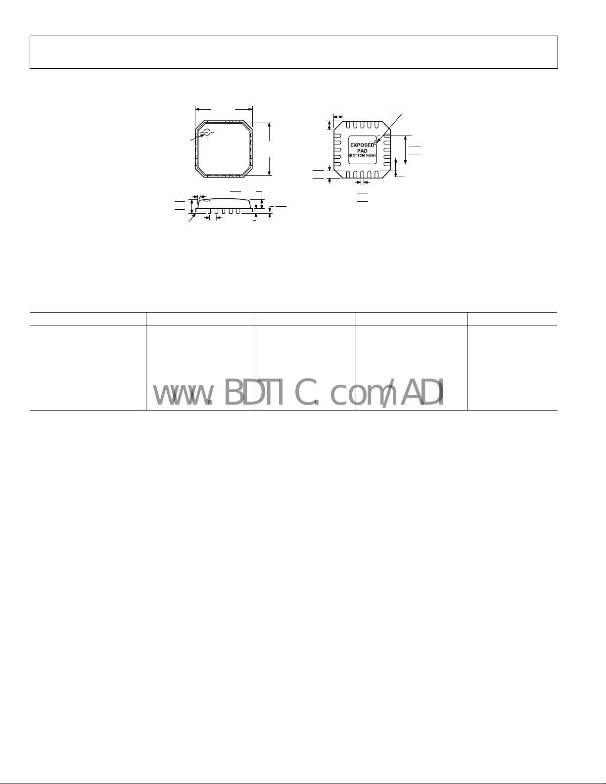
OUTLINE DIMENSIONS
INDICATO
PIN 1
1.00
0.85
0.80
SEATING
PLANE
12° MAX
BSC SQ
0.50
BSC
4.00
TOP
VIEW
0.80 MAX
0.65 TYP
0.20
REF
3.75
BCS SQ
0.05 MAX
0.02 NOM
0.60
MAX
0.60
MAX
0.75
0.55
0.35
COPLANARITY
0.08
16
15
11
10
PIN 1
INDICATOR
20
5
6
0.30
0.23
0.18
1
2.25
2.10 SQ
1.95
0.25 MIN
COMPLIANT TO JEDEC STANDARDS MO-220-VGGD-1
Figure 19. 20-Lead Lead Frame Chip Scale Package [LFCSP_VQ]
4
mm × 4 mm Body, Very Thin Quad
(CP-20-1)
Dimensions shown in millimeters
ORDERING GUIDE
Model Temperature Range Ordering Quantity Package Description Package Option
ADM8839ACP −40°C to +85°C 75 20-Lead LFCSP_VQ CP-20-1
ADM8839ACP-REEL −40°C to +85°C 5,000 20-Lead LFCSP_VQ CP-20-1
ADM8839ACP-REEL7 −40°C to +85°C 1,500 20-Lead LFCSP_VQ CP-20-1
ADM8839ACPZ1 −40°C to +85°C 75 20-Lead LFCSP_VQ CP-20-1
ADM8839ACPZ-REEL1 −40°C to +85°C 5,000 20-Lead LFCSP_VQ CP-20-1
ADM8839ACPZ-REEL71 −40°C to +85°C 1,500 20-Lead LFCSP_VQ CP-20-1
EVAL-ADM8839EB Evaluation Board
1
Z = Pb-free part.
Rev. C | Page 10 of 12

ADM8839
www.BDTIC.com/ADI
NOTES
Rev. C | Page 11 of 12

ADM8839
www.BDTIC.com/ADI
NOTES
©2006 Analog Devices, Inc. All rights reserved. Trademarks and
registered trademarks are the property of their respective owners.
C03075-0-7/06(C)
Rev. C | Page 12 of 12
 Loading...