Analog Devices ADM869LARQ Datasheet

2 A, High-Side P-Channel Switch with
a
FEATURES
2 A Load Current
45 m⍀ On Resistance
User-Settable Current Limit
12 A Typical Quiescent Current
10 nA Typical Shutdown Current
40 nA Typical Switch Off Leakage
Short-Circuit Protection
Thermal Shutdown
FAULT Output
Small, 16-Lead QSOP Package
APPLICATIONS
Desktop Computers
Palmtop Computers
Notebook Computers
Hand-Held Instruments
Universal Serial Bus (USB)
Current Limit and Thermal Shutdown
ADM869L
GENERAL DESCRIPTION
The ADM869L is a logic controlled P-channel switch with low
on resistance, capable of sourcing up to 2 A from supply voltages
between 2.7 V and 5.5 V. A user-settable current limit allows
the trip current to be set between 400 mA and 2 A with an
accuracy of ± 21%. This allows the system power supply to be
protected against short circuits and surge currents in peripheral
loads powered via the ADM869L. Over-current and overtemperature conditions are signalled by a FAULT output.
The ADM869L also offers low quiescent current of typically
12 µA and shutdown current of typically 10 nA.
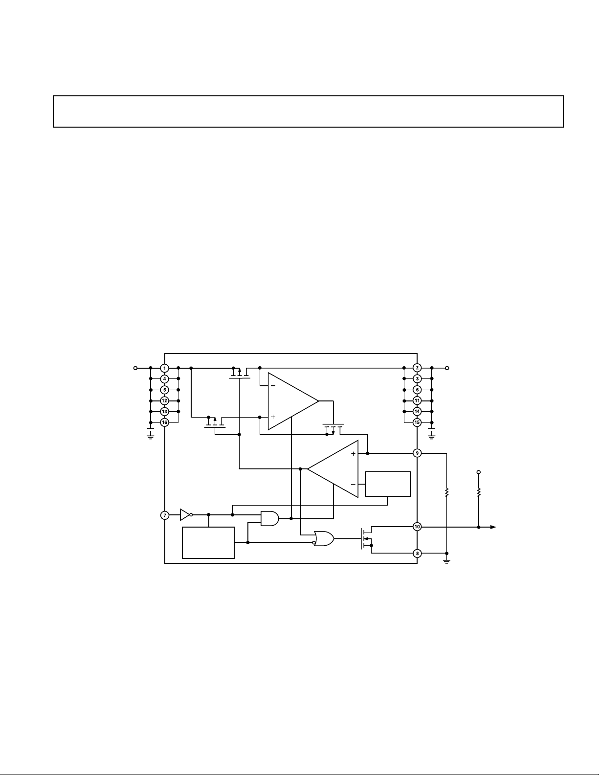
FUNCTIONAL BLOCK DIAGRAM
IN
(2.7V TO 5.5V)
ON
MIRROR FET
ADM869L
ON
TEMPERATURE
SENSOR AND
CONTROL
CIRCUITRY
MAIN FET
OVERTEMP
MIRROR
AMPLIFIER
ON
CURRENT
LIMIT
AMPLIFIER
ON
1.24V
BANDGAP
REFERENCE
ON
SET
FAULT
GND
OUT
0.1F22F
V
PULLUP
0 TO 5.5V
R
R
SET
PULLUP
10k⍀ TO 100k⍀
REV. A
Information furnished by Analog Devices is believed to be accurate and
reliable. However, no responsibility is assumed by Analog Devices for its
use, nor for any infringements of patents or other rights of third parties
which may result from its use. No license is granted by implication or
otherwise under any patent or patent rights of Analog Devices.
One Technology Way, P.O. Box 9106, Norwood, MA 02062-9106, U.S.A.
Tel: 781/329-4700 World Wide Web Site: http://www.analog.com
Fax: 781/326-8703 © Analog Devices, Inc., 2000

ADM869L–SPECIFICATIONS
(VCC = 3.0 V, TA = –40ⴗC to +85ⴗC1, unless otherwise noted.)
Parameter Min Typ Max Unit Test Conditions/Comments
Operating Voltage Range 2.7 5.5 V
Quiescent Current 12 20 µAV
= 5 V, ON = GND, I
IN
OUT
= 0 A,
0°C to 85°C
12 25 µAV
= 5 V, ON = GND, I
IN
OUT
= 0 A,
–40°C to +85°C
Shutdown Supply Current 0.01 2 µA ON = VIN = V
Off-Switch Current 0.04 2 µA ON = V
= VCC, V
IN
OUT
= 5.5 V
= 0 V
OUT
Undervoltage Lockout 2.0 2.3 2.6 V Rising Edge, 1% Hysteresis
On Resistance 38 70 mΩ VIN = 4.75 V
45 90 mΩ V
Nominal Current-Limit Setting Range 0.4 2.4 A R
Current-Limit Amplifier Threshold 1.178 1.240 1.302 V V
I
OUT/ISET
ON Input Low Voltage, V
ON Input High Voltage, V
Current Ratio 810 955 1100 A/A I
IL
IH
2.0 V VIN = 2.7 V to 3.6 V
0.8 V VIN = 2.7 V to 5.5 V
2.4 V V
ON Input Leakage 0.01 ± 1 µAV
Current-Limit Amplifier Input Bias Current 0.05 ± 3 µAV
FAULT Logic Output Low Voltage 0.4 V I
FAULT Output High Leakage Current 0.05 1 µAV
Slow Current-Loop Response Time 10 µs 20% Current Overdrive, V
= 3.0 V
IN
= 1% Tolerance
SET
Required to Turn Off Switch
SET
= 1 A, V
OUT
= 4.5 V to 5.5 V
IN
= 5.5 V
ON
= 1.24 V, I
SET
= 1 mA, V
SINK
FAULT
OUT
= 5.5 V, V
> 1.6 V
= 0 A
OUT
= 1.4 V
SET
SET
2
= 1 V
IN
= 5 V
Fast Current-Loop Response Time 4 µs
Turn-On Time 100 300 µsV
200 µsV
Turn-Off Time 1 2 30 µsV
NOTES
1
Specifications to –40°C are guaranteed by design, not tested.
2
Guaranteed by design. Derived from the I
3
Tested with I
Specifications subject to change without notice.
= 200 mA and V
OUT
SET
current ratio, current-limit amplifier and external set resistor accuracies.
SET
adjusted until (VIN – V
) 艌 0.8 V.
OUT
= 5 V, I
IN
= 3 V, I
IN
= 5 V, I
IN
= 500 mA
OUT
= 500 mA
OUT
= 500 mA
OUT
3
–2–
REV. A

ADM869L
ABSOLUTE MAXIMUM RATINGS*
(TA = 25°C unless otherwise noted)
IN to GND . . . . . . . . . . . . . . . . . . . . . . . . . . . –0.3 V to +6 V
ON, FAULT to GND . . . . . . . . . . . . . . . . . . . –0.3 V to +6 V
SET, OUT to GND . . . . . . . . . . . . . . –0.3 V to (V
+ 0.3 V)
IN
Maximum Continuous Switch Current . . . . . . . . . . . . . . . 3 A
Continuous Power Dissipation (T
= 70°C) . . . . . . . 667 mW
A
QSOP (Derate 8.3 mW/°C above 70°C)
Operating Temperature Range
Industrial (A Version) . . . . . . . . . . . . . . . . –40°C to +85°C
Storage Temperature Range . . . . . . . . . . . . –65°C to +150°C
Lead Temperature (Soldering, 10 sec) . . . . . . . . . . . . . 300°C
ESD Rating (Outputs) . . . . . . . . . . . . . . . . . . . . . . . . . . 15 kV
(Other Pins) . . . . . . . . . . . . . . . . . . . . . . . . . . . . . . . . . 2 kV
*This is a stress rating only; functional operation of the device at these or any other
conditions above those indicated in the operation sections of this specification is
not implied. Exposure to absolute maximum rating conditions for extended
periods of time may affect reliability.
THERMAL CHARACTERISTICS
16-Lead QSOP Package:
= 50°C/W, θ
θ
JA
= 10°C/W
JC
ORDERING GUIDE
Temperature Package Package
Model Range Description Option
ADM869LARQ –40°C to +85°C 16-Lead QSOP RQ-16
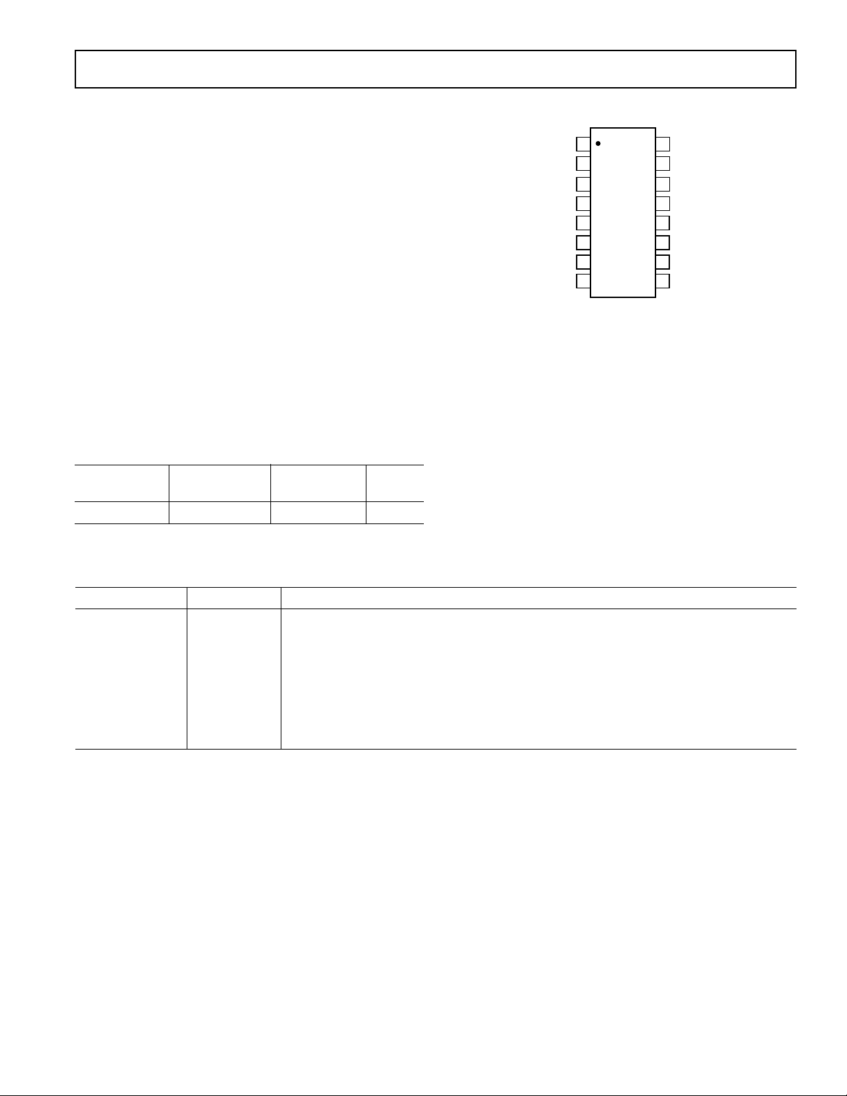
PIN CONFIGURATION
16
15
14
13
12
11
10
9
IN
OUT
OUT
IN
IN
OUT
FAULT
SET
OUT
OUT
OUT
ON
GND
IN
IN
IN
1
2
3
4
ADM869L
TOP VIEW
5
(Not to Scale)
6
7
8
PIN FUNCTION DESCRIPTIONS
Pin Mnemonic Function
1, 4, 5, 12, 13, 16 IN Input to P-Channel MOSFET Source and Supply to Chip Circuitry. Bypass IN with a 22 µF
capacitor to ground.
2, 3, 6, 11, 14, 15 OUT Output from P-Channel MOSFET Drain. Bypass OUT with a 0.1 µF capacitor to ground.
7 ON Digital Input. Active-low switch enable (logic 0 turns the switch on).
9 SET Current Limit Setting Input. A resistor from set to ground sets the current limit. Refer to
Current Limit section.
10 FAULT Open-Drain Digital Output. FAULT goes low when the current limit is exceeded or the die
temperature exceeds 135°C. During startup, FAULT remains low for the turn-on time + 50 µs.
REV. A
–3–
 Loading...