

CMOS Switched-Capacitor
a
FEATURES
ADM660: Inverts or Doubles Input Supply Voltage
ADM8660: Inverts Input Supply Voltage
100 mA Output Current
Shutdown Function (ADM8660)
2.2 mF or 10 mF Capacitors
0.3 V Drop at 30 mA Load
+1.5 V to +7 V Supply
Low Power CMOS: 600 mA Quiescent Current
Selectable Charge Pump Frequency (25 kHz/120 kHz)
Pin Compatible Upgrade for MAX660, MAX665, ICL7660
Available in 16-Lead TSSOP Package
APPLICATIONS
Handheld Instruments
Portable Computers
Remote Data Acquisition
Op Amp Power Supplies
GENERAL DESCRIPTION
The ADM660/ADM8660 is a charge-pump voltage converter
that can be used to either invert the input supply voltage giving
V
= –VIN or double it (ADM660 only) giving V
OUT
Input voltages ranging from +1.5 V to +7 V can be inverted into
a negative –1.5 V to –7 V output supply. This inverting scheme
is ideal for generating a negative rail in single power supply
systems. Only two small external capacitors are needed for the
charge pump. Output currents up to 50 mA with greater than
90% efficiency are achievable, while 100 mA achieves greater
than 80% efficiency.
A Frequency Control (FC) input pin is used to select either
25 kHz or 120 kHz charge-pump operation. This is used to
optimize capacitor size and quiescent current. With 25 kHz
selected, a 10 µF external capacitor is suitable, while with
120 kHz the capacitor may be reduced to 2.2 µF. The oscillator
frequency on the ADM660 can also be controlled with an external capacitor connected to the OSC input or by driving this input with an external clock. In applications where a higher supply
voltage is desired it is possible to use the ADM660 to double
the input voltage. With input voltages from 2.5 V to 7 V, output
voltages from 5 V to 14 V are achievable with up to 100 mA
output current.
The ADM8660 features a low power shutdown (SD) pin instead of the external oscillator (OSC) pin. This can be used to
disable the device and reduce the quiescent current to 300nA.
= 2 × VIN.
OUT
Voltage Converters
ADM660/ADM8660
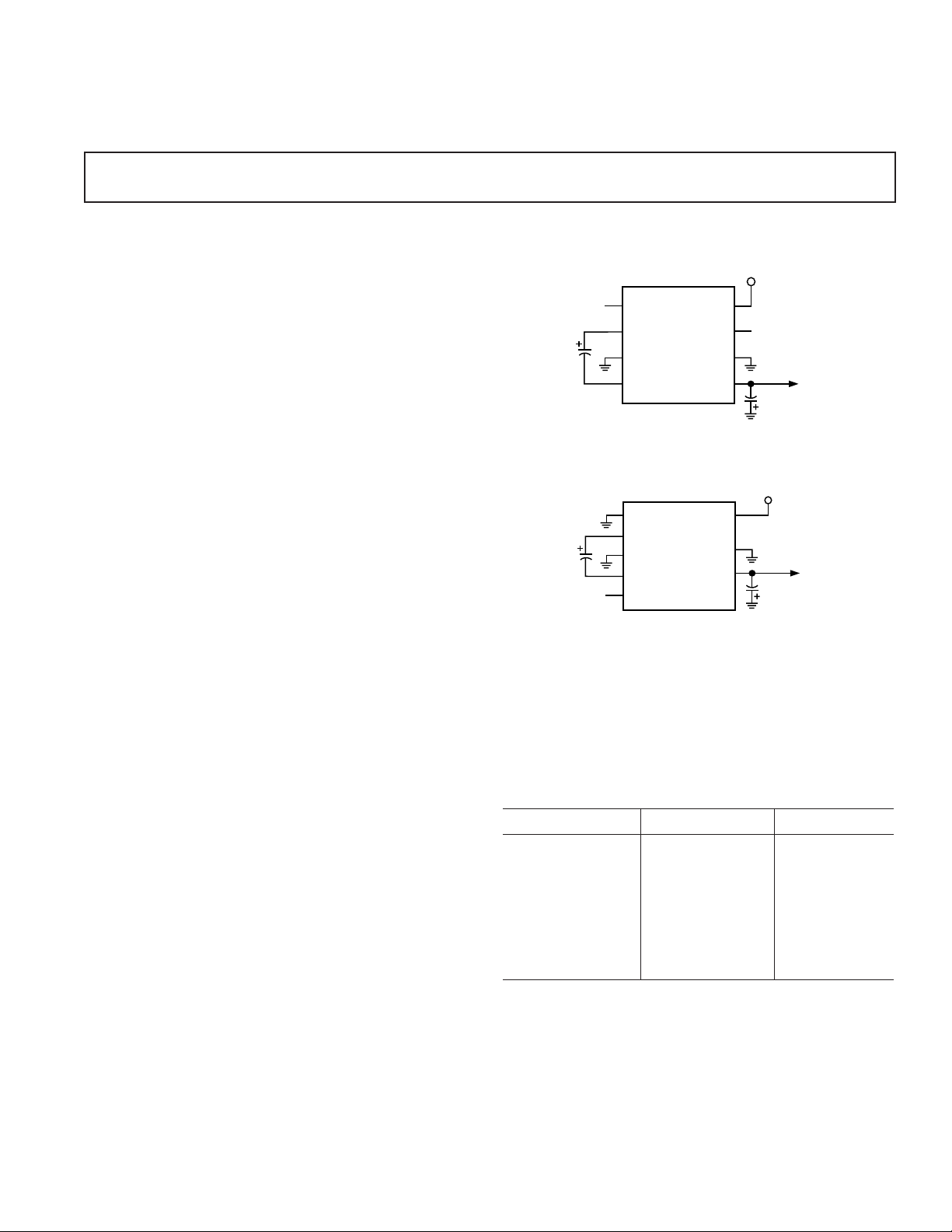
TYPICAL CIRCUIT CONFIGURATIONS
+1.5V TO +7V
INPUT
FC
ADM660
CAP+
10µF
C1
GND
CAP–
Voltage Inverter Configuration (ADM660)
FC
ADM8660
CAP+
C1
10µF
SHUTDOWN
CONTROL
GND
CAP–
SD
Voltage Inverter Configuration with Shutdown (ADM8660)
The ADM660 is a pin compatible upgrade for the MAX660,
MAX665, ICL7660 and LTC1046.
The ADM660/ADM8660 is available in 8-pin DIP and narrowbody SOIC. The ADM660 is also available in a 16-lead TSSOP
package.
ADM660/ADM8660 Options
Option ADM660 ADM8660
Inverting Mode Y Y
Doubling Mode Y N
External Oscillator Y N
Shutdown N Y
Package Options
SO-8 Y Y
N-8 Y Y
RU-16 Y N
V+
OSC
LV
OUT
V+
LV
OUT
C2
10µF
+1.5V TO +7V
INPUT
C2
10µF
INVERTED
NEGATIVE
OUTPUT
INVERTED
NEGATIVE
OUTPUT
REV. A
Information furnished by Analog Devices is believed to be accurate and
reliable. However, no responsibility is assumed by Analog Devices for its
use, nor for any infringements of patents or other rights of third parties
which may result from its use. No license is granted by implication or
otherwise under any patent or patent rights of Analog Devices.
One Technology Way, P.O. Box 9106, Norwood, MA 02062-9106, U.S.A.
Tel: 617/329-4700 World Wide Web Site: http://www.analog.com
Fax: 617/326-8703 © Analog Devices, Inc., 1997
ADM660/ADM8660–SPECIFICATIONS
(V+ = +5 V, C1, C2 = 10 mF,1 TA = T
noted)
MIN
to T
unless otherwise
MAX
Parameter Min Typ Max Units Test Conditions/Comments
Input Voltage, V+ R
= 1 kΩ
L
3.5 7.0 V Inverting Mode, LV = Open
1.5 7.0 V Inverting Mode, LV = GND
2.5 7.0 V Doubling Mode, LV = OUT
Supply Current No Load
0.6 1 mA FC = Open (ADM660), GND (ADM8660)
2.5 4.5 mA FC = V+, LV = Open
Output Current 100 mA
Output Resistance 9 15 Ω IL = 100 mA
Charge-Pump Frequency 25 kHz FC = Open (ADM660), GND (ADM8660)
120 kHz FC = V+
OSC Input Current ±5 µA FC = Open (ADM660), GND (ADM8660)
±25 µA FC = V+
Power Efficiency (FC = Open) 90 94 % R
90 93 % R
81.5 % I
= 1 kΩ Connected from V+ to OUT
L
= 500 Ω Connected from OUT to GND
L
= 100 mA to GND
L
Voltage Conversion Efficiency 99 99.96 % No Load
Shutdown Supply Current, I
Shutdown Input Voltage, V
SHDN
SHDN
2.4 V SHDN High = Disabled
0.3 5 µA ADM8660, SHDN = V+
0.8 V SHDN Low = Enabled
Shutdown Exit Time 500 µsI
NOTES
1
C1 and C2 are low ESR (<0.2 Ω) electrolytic capacitors. High ESR will degrade performance.
Specifications subject to change without notice.
= 100 mA
L
ABSOLUTE MAXIMUM RATINGS*
(TA = +25°C unless otherwise noted)
Input Voltage (V+ to GND, GND to OUT) . . . . . . . . +7.5 V
LV Input Voltage . . . . . . . . . . (OUT – 0.3 V) to (V+, +0.3 V)
FC and OSC Input Voltage
. . . . . . . . . . . (OUT – 0.3 V) or (V+, –6 V) to (V+, +0.3 V)
OUT, V+ Output Current (Continuous) . . . . . . . . . . . 120 mA
Output Short Circuit Duration to GND . . . . . . . . . . . 10 secs
Power Dissipation, N-8 . . . . . . . . . . . . . . . . . . . . . . . 625 mW
(Derate 8.3 mW/°C above +50°C)
θ
, Thermal Impedance . . . . . . . . . . . . . . . . . . . . 120°C/W
JA
Power Dissipation R-8 . . . . . . . . . . . . . . . . . . . . . . . . 450 mW
(Derate 6 mW/°C above +50°C)
θ
, Thermal Impedance . . . . . . . . . . . . . . . . . . . . 170°C/W
JA
Power Dissipation RU-16 . . . . . . . . . . . . . . . . . . . . . 500 mW
(Derate 6 mW/°C above +50°C)
θ
, Thermal Impedance . . . . . . . . . . . . . . . . . . . . 158°C/W
JA
Operating Temperature Range
Industrial (A Version) . . . . . . . . . . . . . . . . –40°C to +85°C
Storage Temperature Range . . . . . . . . . . . –65°C to +150°C
Lead Temperature Range (Soldering 10 sec) . . . . . . . . +300°C
Vapor Phase (60 sec) . . . . . . . . . . . . . . . . . . . . . . . . +215°C
Infrared (15 sec) . . . . . . . . . . . . . . . . . . . . . . . . . . . . +220°C
ESD Rating . . . . . . . . . . . . . . . . . . . . . . . . . . . . . . . . >2000 V
*This is a stress rating only; functional operation of the device at these or any other
conditions above those indicated in the operation section of this specification is not
implied. Exposure to absolute maximum rating conditions for extended periods
may affect device reliability.
ORDERING GUIDE
Temperature Package
Model Range Options*
ADM660AN –40°C to +85°C N-8
ADM660AR –40°C to +85°C SO-8
ADM660ARU –40°C to +85°C RU-16
ADM8660AN –40°C to +85°C N-8
ADM8660AR –40°C to +85°C SO-8
*N = Plastic DIP; RU = Thin Shrink Small Outline; SO = Small Outline.
–2–
REV. A
PIN FUNCTION DESCRIPTIONS
ADM660/ADM8660
Inverter Configuration
Mnemonic Function
FC Frequency Control Input for Internal Oscillator
and Charge Pump. With FC = Open (ADM660)
or connected to GND (ADM8660), f
with FC = V+, f
= 120 kHz
CP
= 25 kHz;
CP
CAP+ Positive Charge-Pump Capacitor Terminal.
GND Power Supply Ground.
CAP– Negative Charge-Pump Capacitor Terminal.
OUT Output, Negative Voltage.
LV Low Voltage Operation Input. Connect to GND
when input voltage is less than 3.5 V. Above
3.5 V, LV may be connected to GND or left
unconnected.
OSC ADM660: Oscillator Control Input. OSC is
connected to an internal 15 pF capacitor. An
external capacitor may be connected to slow the
oscillator. An external oscillator may also be
used to overdrive OSC. The charge-pump
frequency is equal to 1/2 the oscillator frequency.
SD ADM8660: Shutdown Control Input. This in-
put, when high, is used to disable the charge
pump thereby reducing the power consumption.
V+ Positive Power Supply Input.
Doubler Configuration (ADM660 Only)
Mnemonic Function
FC Frequency Control Input for Internal Oscillator
and Charge Pump. With FC = Open, f
25 kHz; with FC = V+, f
= 120 kHz.
CP
CP
=
CAP+ Positive Charge-Pump Capacitor Terminal.
GND Positive Input Supply.
CAP– Negative Charge-Pump Capacitor Terminal.
OUT Ground.
LV Low Voltage Operation Input. Connect to OUT.
OSC Must be left unconnected in this mode.
V+ Doubled Positive Output.
CAP+
GND
CAP–
FC
1
ADM660
2
TOP VIEW
3
(Not to Scale)
4
PIN CONNECTIONS
8-Lead
8
V+
7
OSC
6
LV
5
OUT
CAP+
GND
CAP–
1
FC
2
3
4
16-Lead
1
NC
2
NC
3
FC
4
CAP+
5
6
CAP–
7
NC
8
NC
NC = NO CONNECT
ADM660
RU-16
TOP VIEW
(Not to Scale)
16
NC
15
NC
14
V+
13
OSC
12
LVGND
11
OUT
NC
10
NC
9
ADM8660
TOP VIEW
(Not to Scale)
V+
8
7
SD
6
LV
5
OUT
REV. A
–3–

ADM660/ADM8660–T ypical Performance Characteristics
3
2.5
2
1.5
1
SUPPLY CURRENT – mA
0.5
0
1.5 7.5
VOLTAGE DOUBLER
3.5 5.5
SUPPLY VOLTAGE – Volts
LV = OUT
LV = GND
LV = OPEN
Figure 1. Power Supply Current vs. Voltage
–3
–3.4
–3.8
–4.2
OUTPUT VOLTAGE – Volts
–4.6
–5
0 100
EFFICIENCY
V
OUT
20 40 60 80
LOAD CURRENT – mA
100
80
60
40
EFFICIENCY – %
20
0
100
POWER EFFICIENCY – %
IL = 10mA
90
IL = 1mA
80
70
60
IL = 50mA
50
IL = 80mA
40
30
1k 1M10k 100k
CHARGE-PUMP FREQUENCY – Hz
Figure 4. Efficiency vs. Charge-Pump Frequency
3.5
3
2.5
2
1.5
1
SUPPLY CURRENT – mA
0.5
0
1 100010
CHARGE-PUMP FREQUENCY – kHz
LV = GND
VOLTAGE DOUBLER
LV = GND
VOLTAGE INVERTER
100
Figure 2. Output Voltage and Efficiency vs. Load Current
1.6
1.2
0.8
V+ = +1.5V
OUTPUT VOLTAGE DROP
0.4
FROM SUPPLY VOLTAGE – Volts
0
0 10020
LOAD CURRENT – mA
V+ = +3.5V
V+ = +2.5V
V+ = +5.5V
40 60 80
V+ = +4.5V
Figure 3. Output Voltage Drop vs. Load Current
Figure 5. Power Supply Current vs. Charge-Pump
Frequency
120
100
80
60
EFFICIENCY – %
40
20
0
0 10020 40 60 80
V+ = +1.5V
V+ = +6.5V
V+ = +5.5V
V+ = +2.5V
LOAD CURRENT – mA
V+ = +4.5V
V+ = +3.5V
Figure 6. Power Efficiency vs. Load Current
–4–
REV. A

ADM660/ADM8660
5
4.5
LOAD = 1mA
4
3.5
3
2.5
2
1.5
OUTPUT VOLTAGE – Volts
1
0.5
0
1 100010 100
CHARGE-PUMP FREQUENCY – kHz
LOAD = 10mA
LOAD = 50mA
LOAD = 80mA
Figure 7. Output Voltage vs. Charge-Pump Frequency
30
25
20
15
35
30
25
20
LV = GND
15
10
CHARGE-PUMP FREQUENCY – kHz
5
0
–40 –20 20 40 60 80
FC = OPEN
C1, C2 = 10µF
0
TEMPERATURE – °C
Figure 10. Charge-Pump Frequency vs. Temperature
1k
100
10
FC = OPEN
LV = GND
FC = V+
LV = GND
10
5
OUTPUT SOURCE RESISTANCE – Ω
0
1.5 6.52.5 3.5 4.5 5.5
SUPPLY VOLTAGE – Volts
Figure 8. Output Source Resistance vs. Supply Voltage
30
LV = GND
LV = OPEN
20
FC = OPEN
OSC = OPEN
C1, C2 = 10µF
10
CHARGE-PUMP FREQUENCY – kHz
0
1.5 3.5 5.5
2.5 4.5 6.5
SUPPLY VOLTAGE – Volts
1
CHARGE-PUMP FREQUENCY – kHz
0.1
11k10 100
CAPACITANCE – pF
Figure 11. Charge-Pump Frequency vs. External
Capacitance
140
120
100
80
60
40
CHARGE-PUMP FREQUENCY – kHz
20
0
373.5
LV = GND
LV = OPEN
FC = V+
OSC = OPEN
C1, C2 = 2.2µF
4 4.5 5 5.5 6 6.5
SUPPLY VOLTAGE – Volts
Figure 9. Charge-Pump Frequency vs. Supply Voltage
REV. A
Figure 12. Charge-Pump Frequency vs. Supply Voltage
–5–

ADM660/ADM8660
S1
S
C1
AB
C2
R
L
V1
V2
C2
R
L
V1
V2
R
EQ
REQ = 1/fC1
160
140
120
100
80
LV = GND
60
40
CHARGE-PUMP FREQUENCY – kHz
20
0
–40
FC = V+
C1, C2 = 2.2µF
TEMPERATURE – °C
100–200 20406080
Figure 13. Charge-Pump Frequency vs. Temperature
GENERAL INFORMATION
The ADM660/ADM8660 is a switched capacitor voltage converter that can be used to invert the input supply voltage. The
ADM660 can also be used in a voltage doubling mode. The
voltage conversion task is achieved using a switched capacitor
technique using two external charge storage capacitors. An onboard oscillator and switching network transfers charge between
the charge storage capacitors. The basic principle behind the
voltage conversion scheme is illustrated in Figures 15 and 16.
CAP+
CAP–
÷ 2
S3
C1
S4
Φ2
OUT = –V+
C2
V+
S2
Φ1
OSCILLATOR
60
50
40
30
20
10
OUTPUT SOURCE RESISTANCE – Ω
0
–40 100–200 20406080
V+ = +1.5V
V+ = +3V
V+ = +5V
TEMPERATURE – °C
Figure 14. Output Resistance vs. Temperature
Switched Capacitor Theory of Operation
As already described, the charge pump on the ADM660/
ADM8660 uses a switched capacitor technique in order to
invert or double the input supply voltage. Basic switched
capacitor theory is discussed below.
A switched capacitor building block is illustrated in Figure 17.
With the switch in position A, capacitor C1 will charge to voltage V1. The total charge stored on C1 is q1 = C1V1. The
switch is then flipped to position B discharging C1 to voltage
V2. The charge remaining on C1 is q2 = C1V2. The charge
transferred to the output V2 is, therefore, the difference between q1 and q2, so ∆q = q1–q2 = C1 (V1–V2).
Figure 15. Voltage Inversion Principle
1
CAP+
CAP–
÷ 2
S3
C1
S4
V+
Φ2
V
= 2V+
OUT
C2
V+
S2
Φ1
OSCILLATOR
Figure 16. Voltage Doubling Principle
Figure 15 shows the voltage inverting configuration, while Figure
16 shows the configuration for voltage doubling. An oscillator
generating antiphase signals φ1 and φ2 controls switches S1, S2
and S3, S4. During φ1, switches S1 and S2 are closed charging
C1 up to the voltage at V+. During φ2, S1 and S2 open and S3
and S4 close. With the voltage inverter configuration during φ2,
the positive terminal of C1 is connected to GND via S3 and the
negative terminal of C1 connects to V
is voltage inversion at V
wrt GND. Charge on C1 is trans-
OUT
via S4. The net result
OUT
ferred to C2 during φ2. Capacitor C2 maintains this voltage
during φ1. The charge transfer efficiency depends on the onresistance of the switches, the frequency at which they are being
switched and also on the equivalent series resistance (ESR) of
the external capacitors. The reason for this is explained in the
following section. For maximum efficiency, capacitors with low
ESR are, therefore, recommended.
The voltage doubling configuration reverses some of the connections but the same principle applies.
Figure 17. Switched Capacitor Building Block
As the switch is toggled between A and B at a frequency f, the
charge transfer per unit time or current is
I = f(∆q) = f (C1)(V1–V 2)
Therefore
I =(V1–V2)/(1 /fC1) = (V1–V2)/(REQ)
where REQ = 1/fC1
The switched capacitor may, therefore, be replaced by an
equivalent resistance whose value is dependent on both the
capacitor size and the switching frequency. This explains why
lower capacitor values may be used with higher switching frequencies. It should be remembered that as the switching frequency is increased the power consumption will increase due to
some charge being lost at each switching cycle. As a result, at high
frequencies the power efficiency starts decreasing. Other losses
include the resistance of the internal switches and the equivalent
series resistance (ESR) of the charge storage capacitors.
Figure 18. Switched Capacitor Equivalent Circuit
–6–
REV. A

ADM660/ADM8660
INVERTED
NEGATIVE
OUTPUT
+1.5V TO +7V
INPUT
C1
C2
ADM660
ADM8660
V+
GND
OUT
LV
OSC
FC
CAP+
CAP–
CMOS GATE
CLK OSC
Inverting Negative Voltage Generator
Table II. ADM8660 Charge-Pump Frequency Selection
Figures 19 and 20 show the ADM660/ADM8660 configured to
generate a negative output voltage. Input supply voltages from
1.5 V up to 7 V are allowable. For supply voltage less than 3 V,
LV must be connected to GND. This bypasses the internal
regulator circuitry and gives best performance in low voltage
applications. With supply voltages greater than 3 V, LV may
be either connected to GND or left open. Leaving it open facili-
FC OSC Charge Pump C1, C2
GND Open 25 kHz 10 µF
V+ Open 120 kHz 2.2 µF
GND or V+ Ext Cap See Typical Characteristics
GND Ext CLK Ext CLK Frequency/2
tates direct substitution for the ICL7660.
+1.5V TO +7V
INPUT
FC
ADM660
CAP+
GND
CAP–
10µF
C1
Figure 19. ADM660 Voltage Inverter Configuration
FC
ADM8660
CAP+
C1
10µF
SHUTDOWN
CONTROL
GND
CAP–
SD
Figure 20. ADM8660 Voltage Inverter Configuration
V+
OSC
LV
OUT
V+
LV
OUT
C2
10µF
+1.5V TO +7V
INPUT
C2
10µF
INVERTED
NEGATIVE
OUTPUT
INVERTED
NEGATIVE
OUTPUT
Figure 21. ADM660/ADM8660 External Oscillator
Voltage Doubling Configuration
Figure 22 shows the ADM660 configured to generate increased
output voltages. As in the inverting mode, only two external capacitors are required. The doubling function is achieved by reversing some connections to the device. The input voltage is
applied to the GND pin and V+ is used as the output. Input
voltages from 2.5 V to 7 V are allowable. In this configuration,
pins LV, OUT must be connected to GND.
The unloaded output voltage in this configuration is 2 (V
).
IN
Output resistance and ripple are similar to the voltage inverting
configuration.
OSCILLATOR FREQUENCY
The internal charge-pump frequency may be selected to be
either 25 kHz or 120 kHz using the Frequency Control (FC)
input. With FC unconnected (ADM660) or connected to GND
(ADM8660), the internal charge pump runs at 25 kHz while, if
FC is connected to V+, the frequency is increased by a factor of
five. Increasing the frequency allows smaller capacitors to be
used for equivalent performance or, if the capacitor size is un-
Note that the ADM8660 cannot be used in the voltage
doubling configuration.
+2.5V
TO +7V
INPUT
10µF
FC
CAP+
GND
CAP–
ADM660
V+
OSC
LV
OUT
10µF
DOUBLED
POSITIVE
OUTPUT
changed, it results in lower output impedance and ripple.
If a charge-pump frequency other than the two fixed values is
desired, this is made possible by the OSC input, which can either have a capacitor connected to it or be overdriven by an
external clock. Please refer to the Typical Performance Characteristics, which shows the variation in charge-pump frequency
versus capacitor size. The charge-pump frequency is one-half
the oscillator frequency applied to the OSC pin.
If an external clock is used to overdrive the oscillator, its levels
should swing to within 100 mV of V+ and GND. A CMOS
driver is, therefore, suitable. When OSC is overdriven, FC has
no effect but LV must be grounded.
Note that overdriving is permitted only in the voltage
inverter configuration.
Table I. ADM660 Charge-Pump Frequency Selection
Shutdown Input
The ADM8660 contains a shutdown input that can be used to
disable the device and hence reduce the power consumption. A
logic high level on the SD input shuts the device down reducing
the quiescent current to 0.3 µA. During shutdown the output
voltage goes to 0 V. Therefore, ground referenced loads are
not powered during this state. When exiting shutdown it takes
several cycles (approximately 500 µs) for the charge pump to
reach its final value. If the shutdown function is not being used,
then SD should be hardwired to GND.
Capacitor Selection
The optimum capacitor value selection depends the chargepump frequency. With 25 kHz selected, 10 µF capacitors are
Figure 22. Voltage Doubler Configuration
recommended, while with 120 kHz selected, 2.2 µF capacitors
FC OSC Charge Pump C1, C2
Open Open 25 kHz 10 µF
V+ Open 120 kHz 2.2 µF
Open or V+ Ext Cap See Typical Characteristics
Open Ext CLK Ext CLK Frequency/2
REV. A
may be used. Other frequencies allow other capacitor values to
be used. For maximum efficiency in all cases, it is recommended
that capacitors with low ESR are used for the charge pump.
Low ESR capacitors give both the lowest output resistance and
lowest ripple voltage. High output resistance degrades the overall
power efficiency and causes voltage drops, especially at high
–7–

ADM660/ADM8660
output current levels. The ADM660/ADM8660 is tested using
low ESR, 10 µF, capacitors for both C1 and C2. Smaller values
of C1 increase the output resistance, while increasing C1 will reduce the output resistance. The output resistance is also dependent on the internal switches on resistance as well as the
capacitors ESR so the effect of increasing C1 becomes negligible
past a certain point.
Figure 23 shows how the output resistance varies with oscillator
frequency for three different capacitor values. At low oscillator
frequencies, the output impedance is dominated by the 1/f
C
term. This explains why the output impedance is higher for
smaller capacitance values. At high oscillator frequencies, the
1/f
term becomes insignificant and the output impedance is
C
dominated by the internal switches on resistance. From an output impedance viewpoint, therefore, there is no benefit to be
gained from using excessively large capacitors.
500
400
300
200
OUTPUT RESISTANCE – Ω
100
0
0.1 100110
C1 = C2 = 2.2µF
C1 = C2 = 1µF
C1 = C2 = 10µF
OSCILLATOR FREQUENCY – kHz
Figure 23. Output Impedance vs. Oscillator Frequency
Capacitor C2
The output capacitor size C2 affects the output ripple. Increasing the capacitor size reduces the peak-peak ripple. The ESR
affects both the output impedance and the output ripple.
Reducing the ESR reduces the output impedance and ripple.
For convenience it is recommended that both C1 and C2 be the
same value.
Table III. Capacitor Selection
Bypass Capacitor
The ac impedance of the ADM660/ADM8660 may be reduced
by using a bypass capacitor on the input supply. This capacitor
should be connected between the input supply and GND. It
will provide instantaneous current surges as required. Suitable
capacitors of 0.1 µF or greater may be used.
OUTLINE DIMENSIONS
Dimensions shown in inches and (mm).
8-Lead Plastic DIP
(N-8)
0.430 (10.92)
0.348 (8.84)
8
5
0.280 (7.11)
BSC
0.240 (6.10)
0.060 (1.52)
0.015 (0.38)
0.070 (1.77)
0.045 (1.15)
0.130
(3.30)
MIN
SEATING
PLANE
0.325 (8.25)
0.300 (7.62)
0.195 (4.95)
0.115 (2.93)
0.015 (0.381)
0.008 (0.204)
0.210 (5.33)
MAX
0.160 (4.06)
0.115 (2.93)
0.022 (0.558)
0.014 (0.356)
14
PIN 1
0.100
(2.54)
8-Lead Narrow-Body SOIC
(SO-8)
0.1968 (5.00)
0.1890 (4.80)
8
(1.27)
BSC
5
0.2440 (6.20)
41
0.2284 (5.80)
0.0688 (1.75)
0.0532 (1.35)
0.0192 (0.49)
0.0138 (0.35)
0.0098 (0.25)
0.0075 (0.19)
0.0196 (0.50)
0.0099 (0.25)
8°
0°
0.0500 (1.27)
0.0160 (0.41)
x 45°
0.1574 (4.00)
0.1497 (3.80)
PIN 1
0.0098 (0.25)
0.0040 (0.10)
SEATING
PLANE
0.0500
C2053a–5–5/97
Charge-Pump Capacitor
Frequency C1, C2
25 kHz 10 µF
120 kHz 2.2 µF
Power Efficiency and Oscillator Frequency Tradeoff
While higher switching frequencies allow smaller capacitors to
be used for equivalent performance, or improved performance
with the same capacitors, there is a tradeoff to be considered. As
the oscillator frequency is increased, the quiescent current increases. This happens as a result of a finite charge being lost at
each switching cycle. The charge loss per unit cycle at very high
frequencies can be significant, thereby reducing the power efficiency. Since the power efficiency is also degraded at low oscillator frequencies, due to an increase in output impedance, this
means that there is an optimum frequency band for maximum
power transfer. Please refer to the Typical Performance Characteristics section.
–8–
0.177 (4.50)
0.006 (0.15)
0.002 (0.05)
SEATING
PLANE
0.201 (5.10)
0.193 (4.90)
16 9
0.169 (4.30)
1
PIN 1
0.0118 (0.30)
0.0256
(0.65)
0.0075 (0.19)
BSC
16-Lead TSSOP
(RU-16)
0.256 (6.50)
0.246 (6.25)
8
0.0433
(1.10)
MAX
0.0079 (0.20)
0.0035 (0.090)
8°
0°
PRINTED IN U.S.A.
0.028 (0.70)
0.020 (0.50)
REV. A
 Loading...