Analog Devices ADM8660, ADM660 Datasheet

CMOS Switched-Capacitor
a
FEATURES
ADM660: Inverts or Doubles Input Supply Voltage
ADM8660: Inverts Input Supply Voltage
100 mA Output Current
Shutdown Function (ADM8660)
2.2 mF or 10 mF Capacitors
0.3 V Drop at 30 mA Load
+1.5 V to +7 V Supply
Low Power CMOS: 600 mA Quiescent Current
Selectable Charge Pump Frequency (25 kHz/120 kHz)
Pin Compatible Upgrade for MAX660, MAX665, ICL7660
Available in 16-Lead TSSOP Package
APPLICATIONS
Handheld Instruments
Portable Computers
Remote Data Acquisition
Op Amp Power Supplies
GENERAL DESCRIPTION
The ADM660/ADM8660 is a charge-pump voltage converter
that can be used to either invert the input supply voltage giving
V
= –VIN or double it (ADM660 only) giving V
OUT
Input voltages ranging from +1.5 V to +7 V can be inverted into
a negative –1.5 V to –7 V output supply. This inverting scheme
is ideal for generating a negative rail in single power supply
systems. Only two small external capacitors are needed for the
charge pump. Output currents up to 50 mA with greater than
90% efficiency are achievable, while 100 mA achieves greater
than 80% efficiency.
A Frequency Control (FC) input pin is used to select either
25 kHz or 120 kHz charge-pump operation. This is used to
optimize capacitor size and quiescent current. With 25 kHz
selected, a 10 µF external capacitor is suitable, while with
120 kHz the capacitor may be reduced to 2.2 µF. The oscillator
frequency on the ADM660 can also be controlled with an external capacitor connected to the OSC input or by driving this input with an external clock. In applications where a higher supply
voltage is desired it is possible to use the ADM660 to double
the input voltage. With input voltages from 2.5 V to 7 V, output
voltages from 5 V to 14 V are achievable with up to 100 mA
output current.
The ADM8660 features a low power shutdown (SD) pin instead of the external oscillator (OSC) pin. This can be used to
disable the device and reduce the quiescent current to 300nA.
= 2 × VIN.
OUT
Voltage Converters
ADM660/ADM8660
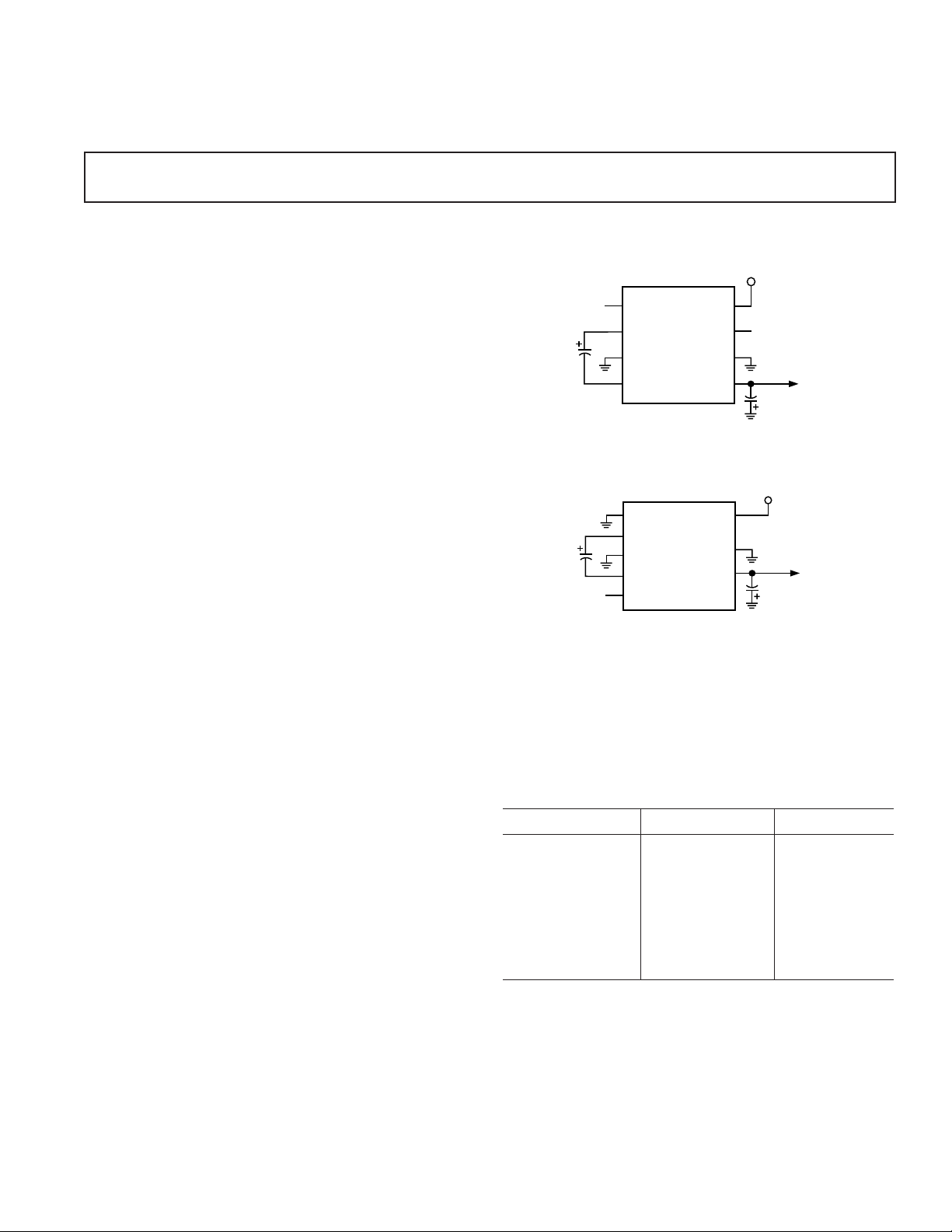
TYPICAL CIRCUIT CONFIGURATIONS
+1.5V TO +7V
INPUT
FC
ADM660
CAP+
10µF
C1
GND
CAP–
Voltage Inverter Configuration (ADM660)
FC
ADM8660
CAP+
C1
10µF
SHUTDOWN
CONTROL
GND
CAP–
SD
Voltage Inverter Configuration with Shutdown (ADM8660)
The ADM660 is a pin compatible upgrade for the MAX660,
MAX665, ICL7660 and LTC1046.
The ADM660/ADM8660 is available in 8-pin DIP and narrowbody SOIC. The ADM660 is also available in a 16-lead TSSOP
package.
ADM660/ADM8660 Options
Option ADM660 ADM8660
Inverting Mode Y Y
Doubling Mode Y N
External Oscillator Y N
Shutdown N Y
Package Options
SO-8 Y Y
N-8 Y Y
RU-16 Y N
V+
OSC
LV
OUT
V+
LV
OUT
C2
10µF
+1.5V TO +7V
INPUT
C2
10µF
INVERTED
NEGATIVE
OUTPUT
INVERTED
NEGATIVE
OUTPUT
REV. A
Information furnished by Analog Devices is believed to be accurate and
reliable. However, no responsibility is assumed by Analog Devices for its
use, nor for any infringements of patents or other rights of third parties
which may result from its use. No license is granted by implication or
otherwise under any patent or patent rights of Analog Devices.
One Technology Way, P.O. Box 9106, Norwood, MA 02062-9106, U.S.A.
Tel: 617/329-4700 World Wide Web Site: http://www.analog.com
Fax: 617/326-8703 © Analog Devices, Inc., 1997

ADM660/ADM8660–SPECIFICATIONS
(V+ = +5 V, C1, C2 = 10 mF,1 TA = T
noted)
MIN
to T
unless otherwise
MAX
Parameter Min Typ Max Units Test Conditions/Comments
Input Voltage, V+ R
= 1 kΩ
L
3.5 7.0 V Inverting Mode, LV = Open
1.5 7.0 V Inverting Mode, LV = GND
2.5 7.0 V Doubling Mode, LV = OUT
Supply Current No Load
0.6 1 mA FC = Open (ADM660), GND (ADM8660)
2.5 4.5 mA FC = V+, LV = Open
Output Current 100 mA
Output Resistance 9 15 Ω IL = 100 mA
Charge-Pump Frequency 25 kHz FC = Open (ADM660), GND (ADM8660)
120 kHz FC = V+
OSC Input Current ±5 µA FC = Open (ADM660), GND (ADM8660)
±25 µA FC = V+
Power Efficiency (FC = Open) 90 94 % R
90 93 % R
81.5 % I
= 1 kΩ Connected from V+ to OUT
L
= 500 Ω Connected from OUT to GND
L
= 100 mA to GND
L
Voltage Conversion Efficiency 99 99.96 % No Load
Shutdown Supply Current, I
Shutdown Input Voltage, V
SHDN
SHDN
2.4 V SHDN High = Disabled
0.3 5 µA ADM8660, SHDN = V+
0.8 V SHDN Low = Enabled
Shutdown Exit Time 500 µsI
NOTES
1
C1 and C2 are low ESR (<0.2 Ω) electrolytic capacitors. High ESR will degrade performance.
Specifications subject to change without notice.
= 100 mA
L
ABSOLUTE MAXIMUM RATINGS*
(TA = +25°C unless otherwise noted)
Input Voltage (V+ to GND, GND to OUT) . . . . . . . . +7.5 V
LV Input Voltage . . . . . . . . . . (OUT – 0.3 V) to (V+, +0.3 V)
FC and OSC Input Voltage
. . . . . . . . . . . (OUT – 0.3 V) or (V+, –6 V) to (V+, +0.3 V)
OUT, V+ Output Current (Continuous) . . . . . . . . . . . 120 mA
Output Short Circuit Duration to GND . . . . . . . . . . . 10 secs
Power Dissipation, N-8 . . . . . . . . . . . . . . . . . . . . . . . 625 mW
(Derate 8.3 mW/°C above +50°C)
θ
, Thermal Impedance . . . . . . . . . . . . . . . . . . . . 120°C/W
JA
Power Dissipation R-8 . . . . . . . . . . . . . . . . . . . . . . . . 450 mW
(Derate 6 mW/°C above +50°C)
θ
, Thermal Impedance . . . . . . . . . . . . . . . . . . . . 170°C/W
JA
Power Dissipation RU-16 . . . . . . . . . . . . . . . . . . . . . 500 mW
(Derate 6 mW/°C above +50°C)
θ
, Thermal Impedance . . . . . . . . . . . . . . . . . . . . 158°C/W
JA
Operating Temperature Range
Industrial (A Version) . . . . . . . . . . . . . . . . –40°C to +85°C
Storage Temperature Range . . . . . . . . . . . –65°C to +150°C
Lead Temperature Range (Soldering 10 sec) . . . . . . . . +300°C
Vapor Phase (60 sec) . . . . . . . . . . . . . . . . . . . . . . . . +215°C
Infrared (15 sec) . . . . . . . . . . . . . . . . . . . . . . . . . . . . +220°C
ESD Rating . . . . . . . . . . . . . . . . . . . . . . . . . . . . . . . . >2000 V
*This is a stress rating only; functional operation of the device at these or any other
conditions above those indicated in the operation section of this specification is not
implied. Exposure to absolute maximum rating conditions for extended periods
may affect device reliability.
ORDERING GUIDE
Temperature Package
Model Range Options*
ADM660AN –40°C to +85°C N-8
ADM660AR –40°C to +85°C SO-8
ADM660ARU –40°C to +85°C RU-16
ADM8660AN –40°C to +85°C N-8
ADM8660AR –40°C to +85°C SO-8
*N = Plastic DIP; RU = Thin Shrink Small Outline; SO = Small Outline.
–2–
REV. A

PIN FUNCTION DESCRIPTIONS
ADM660/ADM8660
Inverter Configuration
Mnemonic Function
FC Frequency Control Input for Internal Oscillator
and Charge Pump. With FC = Open (ADM660)
or connected to GND (ADM8660), f
with FC = V+, f
= 120 kHz
CP
= 25 kHz;
CP
CAP+ Positive Charge-Pump Capacitor Terminal.
GND Power Supply Ground.
CAP– Negative Charge-Pump Capacitor Terminal.
OUT Output, Negative Voltage.
LV Low Voltage Operation Input. Connect to GND
when input voltage is less than 3.5 V. Above
3.5 V, LV may be connected to GND or left
unconnected.
OSC ADM660: Oscillator Control Input. OSC is
connected to an internal 15 pF capacitor. An
external capacitor may be connected to slow the
oscillator. An external oscillator may also be
used to overdrive OSC. The charge-pump
frequency is equal to 1/2 the oscillator frequency.
SD ADM8660: Shutdown Control Input. This in-
put, when high, is used to disable the charge
pump thereby reducing the power consumption.
V+ Positive Power Supply Input.
Doubler Configuration (ADM660 Only)
Mnemonic Function
FC Frequency Control Input for Internal Oscillator
and Charge Pump. With FC = Open, f
25 kHz; with FC = V+, f
= 120 kHz.
CP
CP
=
CAP+ Positive Charge-Pump Capacitor Terminal.
GND Positive Input Supply.
CAP– Negative Charge-Pump Capacitor Terminal.
OUT Ground.
LV Low Voltage Operation Input. Connect to OUT.
OSC Must be left unconnected in this mode.
V+ Doubled Positive Output.
CAP+
GND
CAP–
FC
1
ADM660
2
TOP VIEW
3
(Not to Scale)
4
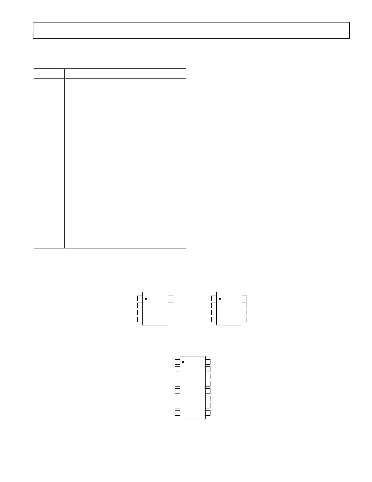
PIN CONNECTIONS
8-Lead
8
V+
7
OSC
6
LV
5
OUT
CAP+
GND
CAP–
1
FC
2
3
4
16-Lead
1
NC
2
NC
3
FC
4
CAP+
5
6
CAP–
7
NC
8
NC
NC = NO CONNECT
ADM660
RU-16
TOP VIEW
(Not to Scale)
16
NC
15
NC
14
V+
13
OSC
12
LVGND
11
OUT
NC
10
NC
9
ADM8660
TOP VIEW
(Not to Scale)
V+
8
7
SD
6
LV
5
OUT
REV. A
–3–
 Loading...