

www.BDTIC.com/ADI
Low Voltage Supervisory Circuits
FEATURES
Precision 1.8 V to 5 V power supply monitoring
RESET
9
4
3 watchdog timeout options
RESET
Low power consumption (5 μA)
Guaranteed reset output valid to V
Power supply glitch immunity
Specified over −40°C t
4-lead SC70 package
APPLICATIONS
Microprocessor systems
Computers
Controllers
Intelligent instruments
Portable equipment
threshold options
1.58 V to 4.63 V
RESET
timeout options
1 ms, 20 ms, 140 ms, 1120 ms
6.3 ms, 102 ms, 1.6 sec
output stages
Push-pull active-low (ADM8616)
Open-drain active-low (ADM8617)
o +85°C temperature range
= 1 V
CC
with Watchdog in 4-Lead SC70
ADM8616/ADM8617
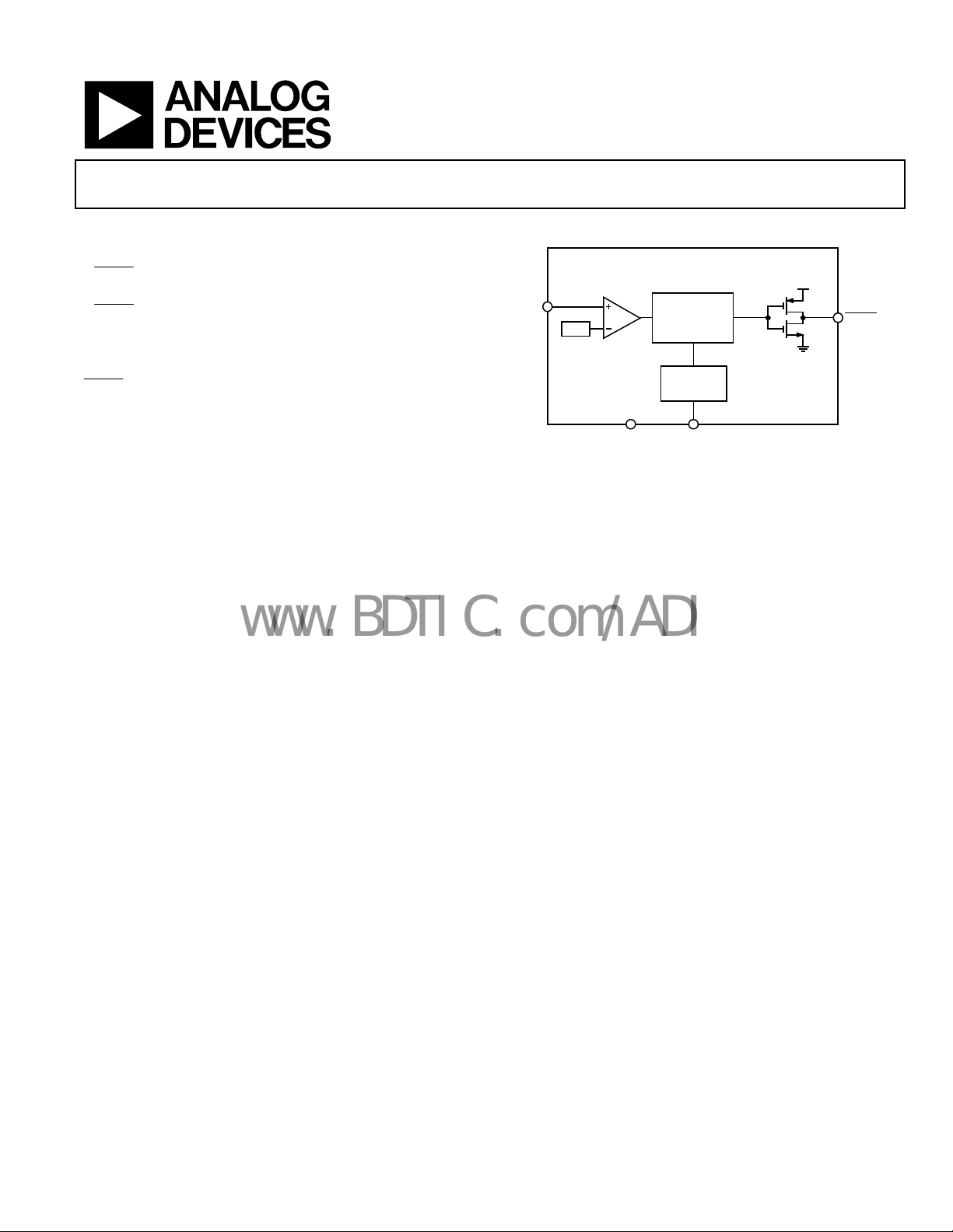
FUNCTIONAL BLOCK DIAGRAM
V
CC
ADM8616
V
REF
RESET
GENERATOR
WATCHDOG
DETECT OR
GND WDI
Figure 1.
V
CC
RESET
4795-001
GENERAL DESCRIPTION
The ADM8616/ADM8617 are supervisory circuits that monitor
power supply voltage levels and code execution integrity in
microprocessor-based systems. A power-on reset signal is
generated when the supply voltage rises to a preset threshold
level. The ADM8616/ADM8617 have an on-chip watchdog
timer that can reset the microprocessor if it fails to strobe
within a preset timeout period.
Each part is available in the following nine reset threshold
ptions: 1.58 V, 1.67 V, 2.19 V, 2.32 V, 2.63 V, 2.93 V, 3.08 V,
o
4.38 V, and 4.63 V. There are four reset timeout options: 1 ms,
20 ms, 140 ms, and 1120 ms. There are also three possible
watchdog timeouts available: 6.3 ms, 102 ms, and 1.6 sec.
Rev. B
Information furnished by Analog Devices is believed to be accurate and reliable. However, no
responsibility is assumed by Anal og Devices for its use, nor for any infringements of patents or ot her
rights of third parties that may result from its use. Specifications subject to change without notice. No
license is granted by implication or otherwise under any patent or patent rights of Analog Devices.
Trademarks and registered trademarks are the property of their respective owners.
The parts differ in terms of reset output configuration. The
AD
M8616 is active-low with a push-pull output, while the
ADM8617 is active-low with an open-drain output.
The ADM8616/ADM8617 are available in 4-lead SC70 packages
nd typically consume only 5 μA, making them suitable for use
a
in low power, portable applications.
One Technology Way, P.O. Box 9106, Norwood, MA 02062-9106, U.S.A.
Tel: 781.329.4700 www.analog.com
Fax: 781.461.3113 ©2007 Analog Devices, Inc. All rights reserved.

ADM8616/ADM8617
www.BDTIC.com/ADI
TABLE OF CONTENTS
Features.............................................................................................. 1
Applications....................................................................................... 1
Functional Block Diagram .............................................................. 1
General Description ......................................................................... 1
Revision History ............................................................................... 2
Specifications..................................................................................... 3
Absolute Maximum Ratings............................................................ 4
ESD Caution.................................................................................. 4
Pin Configuration and Function Descriptions............................. 5
Typical Performance Characteristics ............................................. 6
REVISION HISTORY
1/07—Rev. A to Rev. B
Changes to Functional Block Diagram.......................................... 1
11/06—Rev. 0 to Rev. A
Changes to Ordering Guide.......................................................... 10
6/05—Revision 0: Initial Version
Circuit Description............................................................................8
RESET Output ...............................................................................8
Watchdog Input.............................................................................8
Application Information...................................................................9
Watchdog Input Current ..............................................................9
Negative-Going V
Ensuring RESET Valid to V
Watchdog Software Considerations............................................9
Outline Dimensions....................................................................... 10
Ordering Guide .......................................................................... 10
Transients...................................................9
CC
= 0 V...........................................9
CC
Rev. B | Page 2 of 12
ADM8616/ADM8617
www.BDTIC.com/ADI
SPECIFICATIONS
VCC = full operating range, TA = −40oC to +85oC, unless otherwise noted.
Table 1.
Parameter Min Typ Max Unit Test Conditions/Comments
SUPPLY
VCC Operating Voltage Range 1 5.5 V
Supply Current 10 20 μA VCC = 5.5 V
5 12 μA VCC = 3.6 V
RESET THRESHOLD VOLTAGE
ADM861xL
ADM861xM
ADM861xT
ADM861xS
ADM861xR
ADM861xZ
ADM861xY
ADM861xW
ADM861xV
RESET THRESHOLD TEMPERATURE COEFFICIENT
RESET THRESHOLD HYSTERESIS
RESET TIMEOUT PERIOD
ADM861xxA 1 1.4 2 ms
ADM861xxB 20 28 40 ms
ADM861xxC 140 200 280 ms
ADM861xxD 1120 1600 2240 ms
VCC TO RESET DELAY
RESET OUTPUT VOLTAGE
VOL (Open-Drain and Push-Pull) 0.3 V VCC ≥ 1.0 V, I
0.3 V VCC ≥ 1.2 V, I
0.3 V VCC ≥ 2.7 V, I
0.4 V VCC ≥ 4.5 V, I
VOH (Push-Pull Only) 0.8 × VCC V VCC ≥ 2.7 V, I
RESET Rise Time
Open-Drain RESET Output Leakage Current
WATCHDOG INPUT
Watchdog Timeout Period
ADM861xxxW 4.3 6.3 9.3 ms
ADM861xxxX 71 102 153 ms
ADM861xxxY 1.12 1.6 2.4 sec
WDI Pulse Width 50 ns VIL = 0.3 × VCC, V
WDI Input Threshold V
VIL 0.3 × VCC
VIH 0.7 × VCC V
WDI Input Current 120 160 μA V
4.50 4.63 4.75 V
4.25 4.38 4.50 V
3.00 3.08 3.15 V
2.85 2.93 3.00 V
2.55 2.63 2.70 V
2.25 2.32 2.38 V
2.12 2.19 2.25 V
1.62 1.67 1.71 V
1.52 1.58 1.62 V
40 ppm/°C
2 × V
mV
TH
40 μs V
falling at 1 mV/μs
CC
= 50 μA
SINK
= 100 μA
SINK
= 1.2 mA
SINK
= 3.2 mA
SINK
= 500 μA
SOURCE
VCC − 1.5
V VCC ≥ 4.5 V, I
5 25 ns From 10% to 90% V
SOURCE
= 800 μA
, CL = 5 pF, VCC = 3.3 V
CC
1 μA
= 0.7 × VCC
IH
= VCC
WDI
−20 −15
μA V
WDI
= 0
Rev. B | Page 3 of 12
ADM8616/ADM8617
www.BDTIC.com/ADI
ABSOLUTE MAXIMUM RATINGS
TA = 25°C, unless otherwise noted.
Table 2.
Parameter Rating
VCC
RESET
Output Current (RESET)
Operating Temperature Range
Storage Temperature Range
θJA Thermal Impedance, SC70 146°C/W
Soldering Temperature
Sn/Pb 240°C, 30 sec
Pb-Free 260°C, 40 sec
−0.3 V to +6 V
−0.3 V to +6 V
20 mA
−40°C to +85°C
−65°C to +150°C
Stresses above those listed under Absolute Maximum Ratings
ma
y cause permanent damage to the device. This is a stress
rating only; functional operation of the device at these or any
other conditions above those indicated in the operational
section of this specification is not implied. Exposure to absolute
maximum rating conditions for extended periods may affect
device reliability.
ESD CAUTION
Rev. B | Page 4 of 12

ADM8616/ADM8617
www.BDTIC.com/ADI
PIN CONFIGURATION AND FUNCTION DESCRIPTIONS
GND
1
2
RESET
Figure 2. Pin Configuration
Table 3. Pin Function Descriptions
Pin No. Mnemonic Description
1 GND Ground.
2
RESET
Active-Low RESET Output. Asserted whenever VCC is below the reset threshold (VTH).
Push-Pull Output Stage for ADM8616.
Open-Drain Output Stage for ADM8617.
3 WDI
Watchdog Input. Generates a RESET
if the logic level on the pin remains low or high for the duration of the
watchdog timeout. The timer is cleared if a logic transition occurs on this pin, or if a reset is generated. Leave
floating to disable the watchdog timer.
4 VCC Power Supply Voltage Being Monitored.
ADM8616/
ADM8617
TOP VIEW
(Not to Scale)
V
4
CC
WDI
3
04795-002
Rev. B | Page 5 of 12
ADM8616/ADM8617
www.BDTIC.com/ADI
TYPICAL PERFORMANCE CHARACTERISTICS
10.0
9.5
9.0
8.5
8.0
7.5
7.0
(µA)
6.5
CC
I
6.0
5.5
5.0
4.5
4.0
3.5
1.20
1.15
1.10
1.05
1.00
0.95
0.90
NORMALIZE D RESET TI MEOUT
0.85
0.80
Figure 4. Normalized
100
90
80
70
60
50
40
30
TO RESET DELAY (µs)
CC
V
20
10
0
VCC = 5V
VCC = 3.3V
VCC = 1.5V
TEMPERATURE ( °C)
Figure 3. Supply Current vs. Temperature
TEMPERATURE ( °C)
RESET
Timeout Period vs. Temperature
TEMPERATURE ( °C)
RESET
to
Figure 5. V
CC
Output Delay vs. Temperature
120–40 –20 0 20 40 60 80 100
04795-003
120–40 0–20 4020 1008060
04795-004
120–40 0–20 4020 1008060
04795-005
1.20
1.15
1.10
1.05
1.00
0.95
NORMALIZE D WATCHDOG T IMEOUT
0.90
TEMPERATURE ( °C)
Figure 6. Normalized Watchdog Timeout Period vs. Temperature
1.05
1.04
1.03
1.02
1.01
1.00
0.99
0.98
0.97
NORMALIZE D RESET THRES HOLD
0.96
0.95
TEMPERATURE ( °C)
RESET
Figure 7. Normalized
160
140
120
100
80
60
40
MINIMUM PUL SE WIDTH (µs)
20
VCC = 2.93V
0
Figure 8. Maximum V
RESET THRESHO LD OVERDRI VE (mV)
Transient Duration vs.
CC
Threshold vs. Temperature
VCC = 4.63V
RESET
Threshold Overdrive
120–40 0–20 4020 1008060
04795-006
120–40 0–20 4020 1008060
04795-007
100010 100
04795-008
Rev. B | Page 6 of 12

ADM8616/ADM8617
www.BDTIC.com/ADI
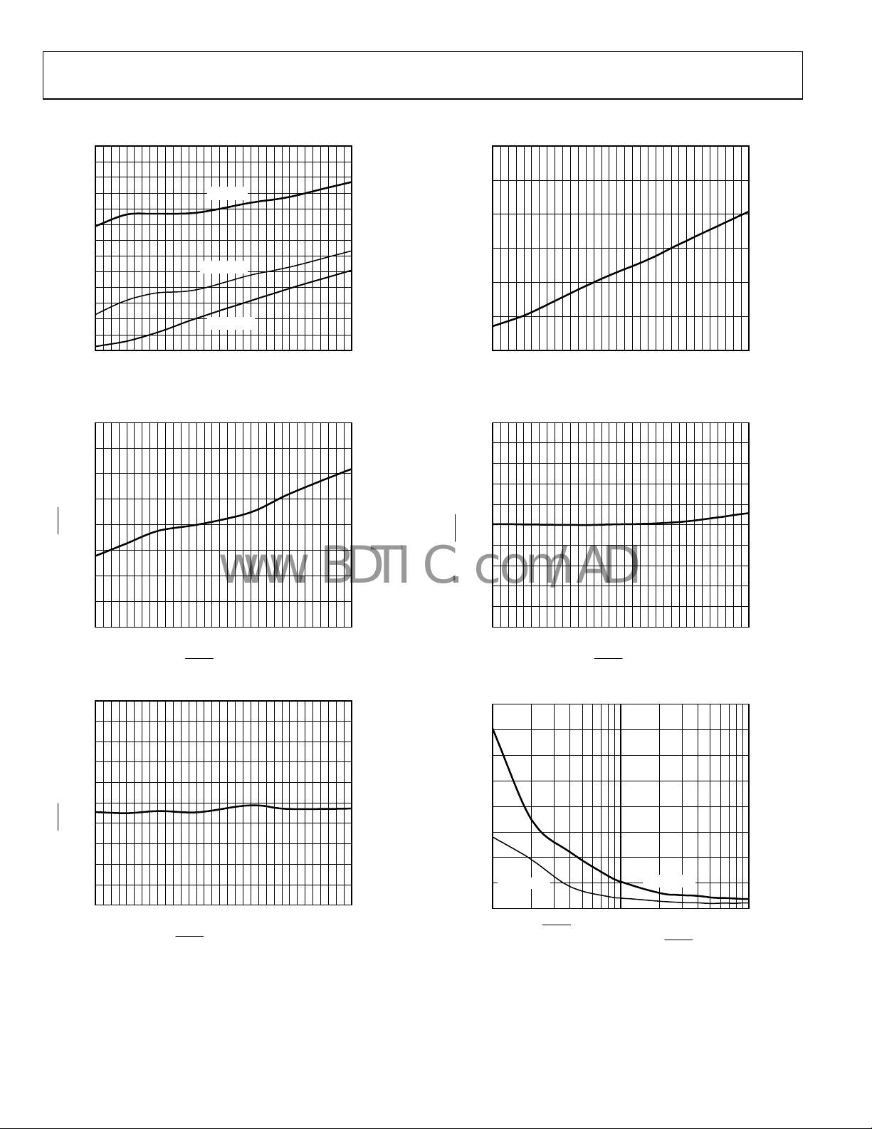
0.20
VCC = 2.9V
2.92
VCC = 2.9V
0.15
(V)
0.10
OUT
V
0.05
0
I
(mA)
SINK
Figure 9. Voltage Output Low vs. I
SINK
75603412
04795-009
2.90
2.88
(V)
OUT
V
2.86
2.84
2.82
I
(mA)
SOURCE
Figure 10. Voltage Output High vs. I
8
SOURCE
1.000.60.0.2 0.4
04795-010
Rev. B | Page 7 of 12

ADM8616/ADM8617
www.BDTIC.com/ADI
CIRCUIT DESCRIPTION
The ADM8616/ADM8617 provide microprocessor supply
voltage supervision by controlling the microprocessors
RESET
input. Code execution errors are avoided during power-up,
power-down, and brownout conditions by asserting a
RESET
signal when the supply voltage is below a preset threshold and
by allowing supply voltage stabilization with a fixed timeout
RESET
after the supply voltage rises above the threshold. In
addition, problems with microprocessor code execution can be
monitored and corrected with a watchdog timer. By including
watchdog strobe instructions in microprocessor code, a watchdog timer can detect if the microprocessor code breaks down or
becomes stuck in an infinite loop. If this happens, the watchdog
timer asserts a
RESET
pulse that restarts the microprocessor in
a known state.
RESET OUTPUT
The ADM8616 features an active-low, push-pull
while the ADM8617 features an active-low, open-drain
output. The
logic high, respectively, for V
The
threshold (V
watchdog timeout period (t
duration of the
above the
RESET
signal is guaranteed to be logic low and
down to 1 V.
CC
RESET
output is asserted when VCC is below the
), or when WDI is not serviced within the
TH
RESET
).
WD
RESET
active timeout period (tRP) after VCC rises
RESET
threshold or after the watchdog timer times
remains asserted for the
out. Figure 11 illustrates the behavior of the
V
V
RESET
CC
CC
1V
0V
V
CC
0V
V
TH
Figure 11.
t
RP
RESET
Timing Diagram
RESET
RESET
V
TH
output,
RESET
RESET
outputs.
t
RD
04795-011
WATCHDOG INPUT
The ADM8616/ADM8617 feature a watchdog timer that
monitors microprocessor activity. A timer circuit is cleared with
every low-to-high or high-to-low logic transition on the watchdog input pin (WDI), which detects pulses as short as 50 ns.
If the timer counts through the preset watchdog timeout period
RESET
(t
),
WD
toggle the WDI pin to avoid being reset. Failure of the microprocessor to toggle WDI within the timeout period, therefore,
indicates a code execution error, and the
restarts the microprocessor in a known state.
In addition to logic transitions on WDI, the watchdog timer
lso cleared by a
is a
condition on V
is cleared and does not begin counting again until
serts. The watchdog timer can be disabled by leaving WDI
floating or by three-stating the WDI driver.
V
RESET
WDI
is asserted. The microprocessor is required to
RESET
RESET
assertion due to an undervoltage
RESET
. When
CC
V
CC
CC
1V
0V
V
CC
0V
V
CC
0V
V
TH
t
RP
Figure 12. Watchdog Timing Diagram
is asserted, the watchdog timer
t
WD
pulse generated
RESET
deas-
t
RD
04795-012
Rev. B | Page 8 of 12

ADM8616/ADM8617
V
V
www.BDTIC.com/ADI
APPLICATION INFORMATION
WATCHDOG INPUT CURRENT
To minimize watchdog input current (and minimize overall
power consumption), leave WDI low for the majority of the
watchdog timeout period. When driven high, WDI can draw as
much as 160 μA. Pulsing WDI low-high-low at a low duty cycle
reduces the effect of the large input current. When WDI is
unconnected, a window comparator disconnects the watchdog
timer from the
RESET
output circuitry so that
RESET
is not asserted when the watchdog timer times out.
NEGATIVE-GOING VCC TRANSIENTS
To avoid unnecessary resets caused by fast power supply
transients, the ADM8616/ADM8617 are equipped with glitch
rejection circuitry. The typical performance characteristic in
Figure 8 plots V
transient duration vs. transient magnitude.
CC
The curve shows combinations of transient magnitude and
duration for which a
RESET
is not generated for 4.63 V and
2.93 V reset threshold parts. For example, with the 2.93 V
threshold, a transient that goes 100 mV below the threshold
and lasts 8 μs typically does not cause a
transient is any bigger in magnitude or duration, a
RESET
, but if the
RESET
is
generated. An optional 0.1 μF bypass capacitor mounted close
to V
provides additional glitch rejection.
CC
ENSURING RESET VALID TO VCC = 0 V
The active-low
as low as 1 V. However, by using an external resistor,
V
CC
valid outputs for V
connected between
when it is unable to sink current. A large resistance, such as
100 kΩ, should be used so that it does not overload the
output when V
RESET
output is guaranteed to be valid for
as low as 0 V are possible. The resistor,
CC
RESET
and ground, pulls the output low
is above 1 V.
CC
CC
RESET
WATCHDOG SOFTWARE CONSIDERATIONS
In implementing the microprocessors watchdog strobe
code, quickly switching WDI low to high and then high to
low (minimizing WDI high time) is desirable for current
consumption reasons. However, a more effective way of
using the watchdog function can be considered.
A low-high-low WDI pulse within a given subroutine prevents
he watchdog from timing out. However, if the subroutine
t
becomes stuck in an infinite loop, the watchdog does not detect
this because the subroutine continues to toggle WDI. A more
effective coding scheme for detecting this error involves using a
slightly longer watchdog timeout. In the program that calls
the subroutine, WDI is set high. The subroutine sets WDI low
when it is called. If the program executes without error, WDI is
toggled high and low with every loop of the program. If the
subroutine enters an infinite loop, WDI is kept low, the watchdog times out, and the microprocessor is reset.
START
SET WDI
HIGH
PROGRAM
CODE
SUBROUTINE
SET WDI
LOW
RETURN
Figure 14. Watchdog Flow Diagram
CC
RESET
INFINITE LOOP:
WATCHDOG
TIMES OUT
04795-014
ADM8616/
ADM8617
Figure 13. Ensuring
RESET
RESET
Valid to VCC = 0 V
100kΩ
4795-013
Rev. B | Page 9 of 12
RESET RESET
ADM8616/
ADM8617
WDI I/O
Figure 15. Typical Application Circuit
µP
04795-015
ADM8616/ADM8617
7
www.BDTIC.com/ADI
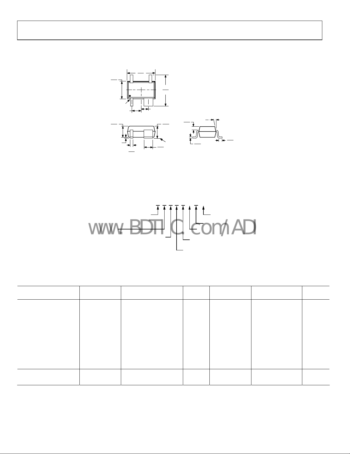
OUTLINE DIMENSIONS
2.20
1.35
1.15
PIN 1
0.65 BSC
1.00
0.80
1.80
4
1
3
2
0.50 BSC
2.40
1.80
1.10
0.80
0.40
0.10
12°
8°
0.30
0.10
0.10 MAX
0.30
0.15
0.10 COPLANARITY
*
PACKAGE OUTLINE CORRESPONDS IN FULL TO EIAJ SC82
EXCEPT FOR WIDTH OF PIN 2 AS SHOWN.
*
0.70
0.50
SEATING
PLANE
0.18
0.10
Figure 16. 4-Lead Thin Shrink Small Outline Transistor Package [SC70]
(K
S-4)
Dimensions shown in millimeters
RESET THRESHO LD
L: 4.63V
M: 4.38V
T: 3.08V
S: 2.93V
R: 2.63V
Z: 2.32V
Y: 2.19V
W: 1.67V
V: 1.58V
ADM861 KS -RL
GENERIC NUMBER
RESET TIMEOUT PERIOD
D: 1120ms (MIN)
Figure 17. Ordering Code Structure
xxxxx x
(6/7)
A: 1ms (MIN)
B: 20ms (MIN)
C: 140ms (MIN)
ORDERING QUANT ITY
RL7: 3,000 PIE CE REEL
Z: LEAD FREE
PACKAGE CODE
KS: 4-LEAD SC70
TEMPERATURE RANG E
A: –40°C TO + 85°C
WATCHDOG TIMEOUT PERIOD
W: 6.3ms (TYP)
X: 102ms (TYP)
Y: 1.6s (T YP)
04795-016
ORDERING GUIDE
1
Model
ADM8616LCYAKSZ-RL7
ADM8616MCYAKSZ-RL724.38
ADM8616TCYAKSZ-RL7
ADM8616SCYAKSZ-RL7
ADM8616RCYAKSZ-RL7
ADM8616ZCYAKSZ-RL7
ADM8616YCYAKSZ-RL7
ADM8616WCYAKSZ-RL721.67
ADM8616VCYAKSZ-RL7
ADM8617SAYAKSZ-RL7
ADM8617RCYAKSZ-RL7
1
If ordering nonstandard models, complete the ordering code shown in Figure 17 by inserting reset threshold, reset timeout, and watchdog timeout suffixes. Contact
Sales for availability of nonstandard models.
2
Z = Pb-free part.
Reset
Threshold (V) Temperature Range Quantity
2
4.63
−40°C to +85°C
−40°C to +85°C
2
3.08
2
2.93
2
2.63
2
2.32
2
2.19
−40°C to +85°C
−40°C to +85°C
−40°C to +85°C
−40°C to +85°C
−40°C to +85°C
−40°C to +85°C
2
1.58
2
2.93
2
2.63
−40°C to +85°C
−40°C to +85°C
−40°C to +85°C
3,000 4-Lead SC70 KS-4 N0F
3,000 4-Lead SC70 KS-4 N0F
3,000 4-Lead SC70 KS-4 N0F
3,000 4-Lead SC70 KS-4 N0F
3,000 4-Lead SC70 KS-4 N0F
3,000 4-Lead SC70 KS-4 N0F
3,000 4-Lead SC70 KS-4 N0F
3,000 4-Lead SC70 KS-4 N0F
3,000 4-Lead SC70 KS-4 N0F
3,000 4-Lead SC70 KS-4 M4X
3,000 4-Lead SC70 KS-4 M4X
Package
Description Package Option Branding
Rev. B | Page 10 of 12

ADM8616/ADM8617
www.BDTIC.com/ADI
NOTES
Rev. B | Page 11 of 12

ADM8616/ADM8617
www.BDTIC.com/ADI
NOTES
©2007 Analog Devices, Inc. All rights reserved. Trademarks and
registered trademarks are the property of their respective owners.
D04795-0-1/07(B)
Rev. B | Page 12 of 12
 Loading...