Low-Voltage Manual Reset & Watchdog
Preliminary Technical Data
ADM8611/ADM8616/ADM8617/ADM8618
FEATURES
Precision 1.8V to 5V Power Supply Monitoring
9 Reset Threshold Options:
1.58V to 4.63V
140ms (Min) Reset Timeout
Manual Reset Input (ADM8611)
Watchdog Timer (ADM8616–ADM8618)
Reset Output Stages
Push-Pull Active-Low
Open-Drain Active-Low
Push-Pull Active-High
Low Power Consumption (3µA)
Guaranteed Reset Output valid to V
CC
=1V
Power Supply Glitch Immunity
Specified Over -40°C to +85°C Temperature Range
4-Lead SC70 Package
APPLICATIONS
Microprocessor Systems
Computers
Controllers
Intelligent Instruments
Portable Equipment
GENERAL DESCRIPTION
The ADM8611/ADM8616/ADM8617/ADM8618 are
supervisory circuits which monitor power supply voltage levels
and code execution integrity in microprocessor-based systems.
A power-on-reset signal is generated when the supply voltage
rises to a preset threshold level. The ADM8611’s debounced
manual reset input can be used to initiate a reset by means of an
external push-button or logic signal. The ADM8616–ADM8618
have an on-chip watchdog timer which can reset the
microprocessor if it fails to strobe within a preset timeout
period.
Table 1. Selection Table
Part No. Manual Reset Watchdog
ADM8611 Yes - Push-Pull
ADM8616 - Yes Push-Pull
ADM8617 - Yes Open-Drain
ADM8618 - Yes Push-Pull
Supervisory Circuits in 4-Lead SC70
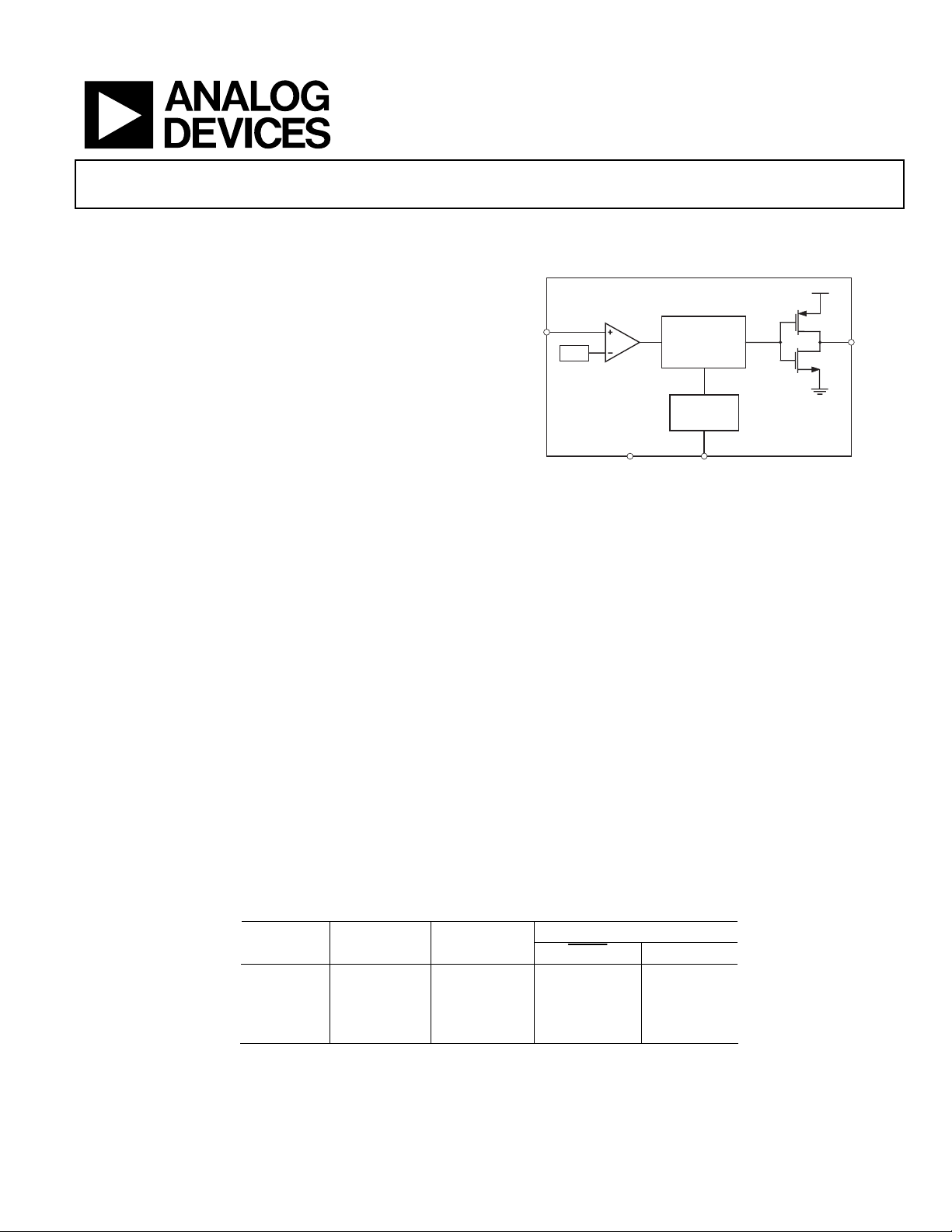
FUNCTIONAL BLOCK DIAGRAMS
V
ADM8616
V
CC
V
REF
GND
RESET
GENERATOR
WATCHDOG
DETECTOR
WDI
Figure 1.
Each part is available in a choice of the following 9 reset
threshold options: 1.58V, 1.67V, 2.19V, 2.32V, 2.63V, 2.93V,
3.08V, 4.38V and 4.63V. The reset timeout periods are 20ms
(min) and 140ms (min) for the ADM8611 and ADM8616–
ADM8618, respectively. The watchdog timeout period is 1.6s
(typ). The parts differ in terms of reset output configuration, as
indicated in table 1.
The ADM8611/ADM8616/ADM8617/ADM8618 are available
in 4-lead SC70 packages and typically consume only 3µA,
making them suitable for use in low power portable
applications.
Output Stage
RESET
RESET
CC
RESET
Rev. PrB
Information furnished by Analog Devices is believed to be accurate and reliable.
However, no responsibility is assumed by Analog Devices for its use, nor for any
infringements of patents or other rights of third parties that may result from its use.
Specifications subject to change without notice. No license is granted by implication
or otherwise under any patent or patent rights of Analog Devices. Trademarks and
registered trademarks are the property of their respective companies.
One Technology Way, P.O. Box 9106, Norwood, MA 02062-9106, U.S.A.
Tel: 781.329.4700
Fax: 781.326.8703 © 2004 Analog Devices, Inc. All rights reserved.
www.analog.com

ADM8611/ADM8616/ADM8617/ADM8618 Preliminary Technical Data
ADM8611/ADM8616/ADM8617/ADM8618—SPECIFICATIONS
Table 2. VCC=Full Operating Range, TA=T
Parameter Min Typ Max Units Test Conditions/Comments
SUPPLY
VCC Operating Voltage Range 1 5.5 V
Supply Current 10 20 µA VCC=5.5V
5 12 µA VCC=3.6V
RESET THRESHOLD VOLTAGE
ADM861_L
ADM861_M
ADM861_T
ADM861_S
ADM861_R
ADM861_Z
ADM861_Y
ADM861_W
ADM861_V
RESET THRESHOLD TEMPERATURE COEFFICIENT 40 ppm/°C
RESET THRESHOLD HYSTERESIS 3 mV
RESET TIMEOUT PERIOD 20 30 40 ms ADM8611
140 200 280 ms ADM8616–ADM8618
VCC TO RESET DELAY 40 µs V
PUSH-PULL OUTPUT (ADM8611, ADM8616, ADM8618)
RESET
Output Voltage
0.3 V VCC>=1.2V, I
0.3 V VCC>=2.7V, I
0.4 V VCC>=4.5V, I
0.8x VCC V VCC>=2.7V, I
V
RESET
Rise Time
RESET Output Voltage 0.3 V VCC>=2.7V, I
0.4 V VCC>=4.5V, I
0.8x VCC V VCC>=1.8V, I
0.8x VCC V VCC>=2.7V, I
V
OPEN-DRAIN OUTPUT (ADM8617)
RESET
Output Voltage
0.3 V VCC>=1.2V, I
0.3 V VCC>=2.7V, I
0.4 V VCC>=4.5V, I
Open-Drain Reset Output Leakage Current 1 µA
MIN
to T
, unless otherwise noted
MAX
4.50 4.63 4.75 V TA=-40°C to +85°C
4.25 4.38 4.50 V TA=-40°C to +85°C
3.00 3.08 3.15 V TA=-40°C to +85°C
2.85 2.93 3.00 V TA=-40°C to +85°C
2.55 2.63 2.70 V TA=-40°C to +85°C
2.25 2.32 2.38 V TA=-40°C to +85°C
2.12 2.19 2.25 V TA=-40°C to +85°C
1.62 1.67 1.71 V TA=-40°C to +85°C
1.52 1.58 1.62 V TA=-40°C to +85°C
0.3 V VCC>=1.0V, I
-1.5 V VCC>=4.5V, I
CC
5 25 ns
-1.5 VCC>=4.5V, I
CC
0.3 V V
falling at 1mV/µs
CC
=50µA
SINK
=100µA
SINK
=1.2mA
SINK
=3.2mA
SINK
=500µA
SOURCE
=800µA
SOURCE
From 10% to 90% V
=3.3V
V
CC
=1.2mA
SINK
=3.2mA
SINK
=150µA
SOURCE
=500µA
SOURCE
=800µA
SOURCE
>=1.0V, I
CC
=50µA
SINK
=100µA
SINK
=1.2mA
SINK
=3.2mA
SINK
, CL=5pF,
CC
Rev. PrB | Page 2 of 7

Preliminary Technical Data ADM8611/ADM8616/ADM8617/ADM8618
Parameter Min Typ Max Units Test Conditions/Comments
MANUAL RESET INPUT (ADM8611)
MR Input Threshold
0.7xVCC V
MR Input Pulse Width
MR Glitch Rejection
MR Pull-up Resistance
MR to Reset Delay
WATCHDOG INPUT (ADM8616, ADM8617, ADM8618)
Watchdog Timeout Period 4.3 6.3 9.3 ms ADM86___W
71 102 153 ms ADM86___X
1.12 1.6 2.4 s ADM86___Y
17.9 25.6 38.4 s ADM86___Z
WDI Pulse Width 50 ns VIL=0.3xVCC, VIH=0.7xVCC,
WDI Input Threshold 0.3xVCC V
0.7xVCC V
WDI Input Current 120 160 µA V
0.3xVCC V
1 µs
100 ns
25 50 75
200 ns
-20 -15 µA V
k⍀
= VCC, time average
WDI
=0, time average
WDI
ABSOLUTE MAXIMUM RATINGS
Table 3. TA = 25°C unless otherwise noted.
Parameter Rating
VCC -0.3V to +6V
RESET
/RESET
Output Current (RESET,
Operating Temperature Range -40°C to +85°C
Storage Temperature Range -65°C to +150°C
θJA Thermal Impedance, SC70
Lead Temperature
Soldering (10 sec) 300°C
Vapour Phase (60 sec) 215°C
Infrared (15 sec) 220°C
RESET
)
-0.3V to +6V
20mA
146°C/W
Stresses above those listed under Absolute Maximum Ratings
may cause permanent damage to the device. This is a stress
rating only and functional operation of the device at these or
any other conditions above those indicated in the operational
section of this specification is not implied. Exposure to absolute
maximum rating conditions for extended periods may affect
device reliability.
Rev. PrB | Page 3 of 7
 Loading...