

Supervisory Circuits with Watchdog and
FEATURES
Manual Reset in 5-Lead SC70 and SOT-23
ADM823/ADM824/ADM825
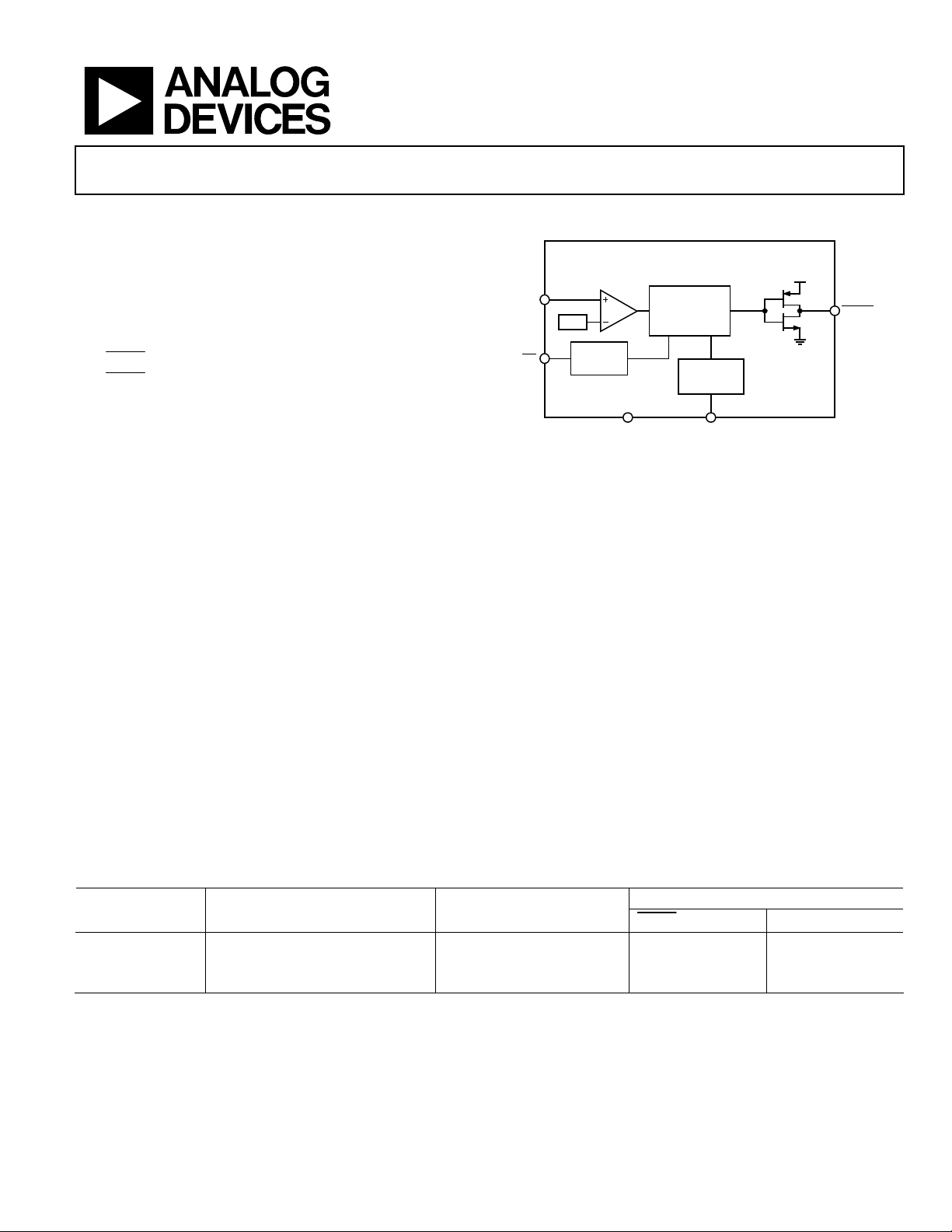
FUNCTIONAL BLOCK DIAGRAM
Precision 2.5 V to 5 V power supply monitor
7 reset threshold options: 2.19 V to 4.63 V
140 ms (min) reset timeout
Watchdog timer with 1.6s timeout (ADM823, ADM824)
Manual reset input (ADM823, ADM825)
V
CC
ADM823
V
REF
RESET
GENERATOR
V
CC
RESET
Push-pull output stages:
(ADM823)
RESET
, RESET (ADM824/ADM825)
RESET
MR
DEBOUNCE
WATCHDOG
DETECTOR
Low power consumption (5 µA)
Guaranteed reset output valid to V
Power supply glitch immunity
Specified over automotive temperature range
5-lead SC70 and SOT-23 packages
= 1 V
CC
GND WDI
Figure 1.
04534-0-001
APPLICATIONS
Microprocessor systems
Computers
Controllers
Intelligent instruments
Portable equipment
GENERAL DESCRIPTION
The ADM823/ADM824/ADM825 are supervisory circuits
which monitor power supply voltage levels and code execution
integrity in microprocessor-based systems. As well as providing
power on reset signals, an on-chip watchdog timer can reset the
microprocessor if it fails to strobe within a preset timeout
period. A reset signal can also be asserted by an external pushbutton, through a manual reset input. The three parts feature
Each part is available in a choice of seven reset threshold
options ranging from 2.19 V to 4.63 V. The reset and watchdog
timeout periods are fixed at 140 ms (min) and 1.6s (typ),
respectively.
The ADM823/ADM824/ADM825 are available in 5-lead SC70
and SOT-23 packages and typically consume only 3 µA, making
them suitable for use in low power portable applications.
different combinations of watchdog input, manual reset input
and output stage configuration, as shown in Table 1.
Table 1. Selection Table
Output Stage
Part No. Watchdog Timer Manual Reset
RESET
RESET
ADM823 Yes Yes Push-Pull –
ADM824 Yes – Push-Pull Push-Pull
ADM825 – Yes Push-Pull Push-Pull
Rev. 0
Information furnished by Analog Devices is believed to be accurate and reliable.
However, no responsibility is assumed by Analog Devices for its use, nor for any
infringements of patents or other rights of third parties that may result from its use.
Specifications subject to change without notice. No license is granted by implication
or otherwise under any patent or patent rights of Analog Devices. Trademarks and
registered trademarks are the property of their respective owners.
One Technology Way, P.O. Box 9106, Norwood, MA 02062-9106, U.S.A.
Tel: 781.329.4700
Fax: 781.326.8703 © 2004 Analog Devices, Inc. All rights reserved.
www.analog.com

ADM823/ADM824/ADM825
TABLE OF CONTENTS
Specifications..................................................................................... 3
Watch d og I nput .............................................................................9
Absolute Maximum Ratings............................................................ 5
ESD Caution.................................................................................. 5
Pin Configurations and Function Descriptions ........................... 6
Typical Performance Characteristics ............................................. 7
Circuit Description........................................................................... 9
Reset Output ................................................................................. 9
Manual Reset Input ...................................................................... 9
REVISION HISTORY
10/04—Revision 0: Initial Version
Application Information................................................................ 10
Watch d og I nput C ur r ent ........................................................... 10
Negative-Going V
Ensuring Reset Valid to V
Watchdog Software Considerations......................................... 10
Outline Dimensions ....................................................................... 11
Ordering Guides......................................................................... 11
Transie n t s ................................................ 10
CC
= 0 V........................................... 10
CC
Rev. 0 | Page 2 of 12

ADM823/ADM824/ADM825
SPECIFICATIONS
VCC = 4.75 V to 5.5 V for ADM82_L, VCC = 4.5 V to 5.5 V for ADM82_M, VCC = 3.15 V to 3.6 V for ADM82_T,
= 3 V to 3.6 V for ADM82_S, VCC = 2.7 V to 3.6 V for ADM82_R, VCC = 2.38 V to 2.75 V for ADM82_Z,
V
CC
V
= 2.25 V to 2.75 V for ADM82_Y, TA = T
CC
Table 2.
Parameter Min Typ Max Unit Test Conditions/Comments
SUPPLY
VCC Operating Voltage Range 1 5.5 V TA = 0°C to +70°C
1.2 V TA = T
Supply Current 10 24 µA
5 12 µA
RESET THRESHOLD VOLTAGE
ADM82_L
4.50 4.75 V TA = T
ADM82_M
4.25 4.50 V TA = T
ADM82_T
3.00 3.15 V TA = T
ADM82_S
2.85 3.00 V TA = T
ADM82_R
2.55 2.70 V TA = T
ADM82_Z (SC70 only)
2.25 2.38 V TA = T
ADM82_Y (SC70 only)
2.13 2.25 V TA = T
RESET THRESHOLD TEMPERATURE COEFFICIENT 40 ppm/°C
RESET THRESHOLD HYSTERESIS 10 mV ADM82_L/M
5 mV ADM82_T/S/R/Z/Y
RESET TIMEOUT PERIOD 140 200 280 ms
VCC TO RESET DELAY 40 µs VTH – VCC = 100 mV
RESET Output Voltage
0.3 V
0.3 V
V
0.8 × V
RESET Output Voltage 0.4 V
0.3 V
0.8 × V
MIN
to T
, unless otherwise noted.
MAX
WDI and
ADM82_L/M
WDI and
ADM82_T/S/R/Z/Y
4.56 4.63 4.70 V TA = 25°C
4.31 4.38 4.45 V TA = 25°C
3.04 3.08 3.11 V TA = 25°C
2.89 2.93 2.96 V TA = 25°C
2.59 2.63 2.66 V TA = 25°C
2.28 2.32 2.35 V TA = 25°C
2.16 2.19 2.22 V TA = 25°C
0.4 V
V
CC
ADM82_L/M
V
CC
ADM82_T/S/R/Z/Y
= 0°C to 70°C, VCC = 1 V,
T
A
V
CC
− 1.5 V
CC
V
CC
ADM82_L/M
V
CC
V
CC
ADM82_T/S/R/Z/Y
V
CC
ADM824L/M, ADM825L/M
V
CC
ADM824T/S/R/Z/Y,
ADM825T/S/R/Z/Y
V
CC
V
CC
to T
MIN
MAX
MR unconnected
MR unconnected
to T
MIN
MAX
to T
MIN
MAX
to T
MIN
MAX
to T
MIN
MAX
to T
MIN
MAX
to T
MIN
MAX
to T
MIN
MAX
= VTH min, I
= VTH min, I
falling, I
SINK
= VTH max, I
= VTH max, I
= VTH max, I
= VTH max, I
≥ 1.8 V, I
SOURCE
= 3.2 mA,
SINK
= 1.2 mA,
SINK
= 50 µA
= 120 µA,
SOURCE
= 30 µA,
SOURCE
= 3.2 mA,
SINK
= 1.2 mA,
SINK
= 150 µA
Rev. 0 | Page 3 of 12
ADM823/ADM824/ADM825
Parameter Min Typ Max Unit Test Conditions/Comments
WATCHDOG INPUT (ADM823, ADM824)
Watchdog Timeout Period 1.12 1.6 2.40 s
WDI Pulse Width 50 ns VIL = 0.4 V, V
WDI Input Threshold
V
IL
WDI Input Current 120 160 µA V
MANUAL RESET INPUT (ADM823, ADM825)
MR Input Threshold
0.7 × V
MR Input Pulse Width
MR Glitch Rejection
MR Pull-Up Resistance
MR to Reset Delay
0.7 × V
−20 −15 µA V
0.3 × V
0.3 × V
CC
V
CC
V
CC
V
CC
= VCC, time average
WDI
= 0, time average
WDI
= 0.8 × V
IH
CC
1 µs
100 ns
35 52 75 kΩ
500 ns
Rev. 0 | Page 4 of 12

ADM823/ADM824/ADM825
ABSOLUTE MAXIMUM RATINGS
TA = 25°C, unless otherwise noted.
Table 3.
Parameter Rating
V
CC
Output Current (RESET, RESET)
All Other Pins –0.3 V to (VCC + 0.3 V)
Operating Temperature Range –40°C to +125°C
Storage Temperature Range –65°C to +150°C
θJA Thermal Impedance
SC70 146°C/W
SOT-23 270°C/W
Lead Temperature
Soldering (10 s) 300°C
Vapor Phase (60 s) 215°C
Infrared (15 s) 220°C
–0.3 V to +6 V
20 mA
ESD CAUTION
ESD (electrostatic discharge) sensitive device. Electrostatic charges as high as 4000 V readily accumulate on
the human body and test equipment and can discharge without detection. Although this product features
proprietary ESD protection circuitry, permanent damage may occur on devices subjected to high energy
electrostatic discharges. Therefore, proper ESD precautions are recommended to avoid performance
degradation or loss of functionality.
Stresses above those listed under Absolute Maximum Ratings
may cause permanent damage to the device. This is a stress
rating only and functional operation of the device at these or
any other conditions above those indicated in the operational
section of this specification is not implied. Exposure to absolute
maximum rating conditions for extended periods may affect
device reliability.
Rev. 0 | Page 5 of 12

ADM823/ADM824/ADM825
PIN CONFIGURATIONS AND FUNCTION DESCRIPTIONS
RESET
GND
MR
1
ADM823
2
TOP VIEW
(Not to Scale)
3
V
5
CC
4
WDI
Figure 2. ADM823 Pin Configuration
04534-0-002
RESET
GND
RESET
1
ADM824
2
TOP VIEW
(Not to Scale)
3
5
4
Figure 3. ADM824 Pin Configuration
Table 4. Pin Function Descriptions
Pin. No. Mnemonic Description
1
RESET
Push-Pull Active-Low Reset Output. Asserted whenever VCC is below the reset threshold, VTH.
2 GND Ground.
3
MR (ADM823) Manual Reset Input. This is an active-low input which, when forced low for at least 1 µs, generates
a reset. It features a 52 kV internal pull-up.
RESET (ADM824/ADM825) Active-High, Push-Pull Reset Output.
4 WDI (ADM823/ADM824)
Watchdog Input. Generates a reset if the voltage on the pin remains low or high for the duration
of the watchdog timeout. The timer is cleared if a logic transition occurs on this pin or if a reset is
generated.
5 V
MR (ADM825)
CC
Manual Reset Input.
Power Supply Voltage Being Monitored.
V
WDI
RESET
GND
RESET
1
ADM825
2
TOP VIEW
(Not to Scale)
3
CC
04534-0-003
V
5
CC
4
MR
04534-0-004
Figure 4. ADM825 Pin Configuration
Rev. 0 | Page 6 of 12

ADM823/ADM824/ADM825
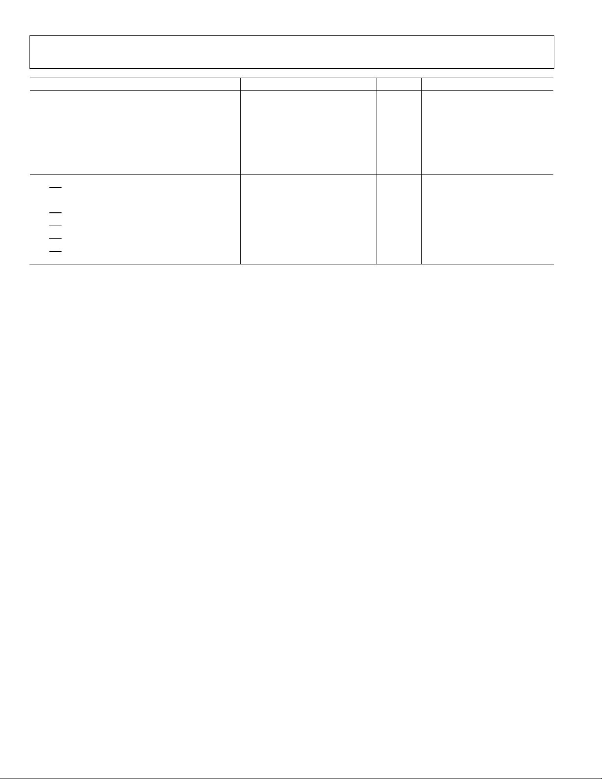
TYPICAL PERFORMANCE CHARACTERISTICS
10.0
9.5
9.0
8.5
ADM823L
8.0
7.5
7.0
(µA)
6.5
CC
I
6.0
ADM824Y
5.5
5.0
4.5
4.0
3.5
ADM825R
TEMPERATURE (°C)
120–40–200 20406080100
04534-0-005
Figure 5. Supply Current vs. Temperature
100
90
80
70
60
50
40
30
TO RESET DELAY (µs)
CC
V
20
10
0
TEMPERATURE (°C)
Figure 8. Reset Comparator Propagation Delay vs. Temperature (V
120–40 40200–20 60 80 100
CC
04534-0-008
Falling)
80
75
70
65
60
55
50
45
40
(µA)
35
CC
I
30
25
20
15
10
5
0
VCC (V)
Figure 6. Supply Current vs. Supply Voltage
1.05
1.04
1.03
1.02
1.01
1.00
0.99
0.98
0.97
NORMALIZED RESET THRESHOLD
0.96
0.95
TEMPERATURE (°C)
Figure 7. Normalized Reset Threshold vs. Temperature
340
320
300
280
260
240
220
200
180
160
140
MANUAL RESET TO RESET DELAY (ns)
120
5.50 2.01.51.00.5 2.5 3.0 3.5 4.0 4.5 5.0
04534-0-006
100
TEMPERATURE (°C)
Figure 9. Manual Reset to Reset Propagation Delay vs. Temperature
120–40 40200–20 60 80 100
04534-0-009
(ADM823/ADM825)
250
240
230
220
210
200
RESET TIMEOUT
190
180
120–40 40200–20 60 80 100
04534-0-007
170
TEMPERATURE (°C)
120–40 40200–20 60 80 100
04534-0-010
Figure 10. Reset Timeout Period vs. Temperature
Rev. 0 | Page 7 of 12
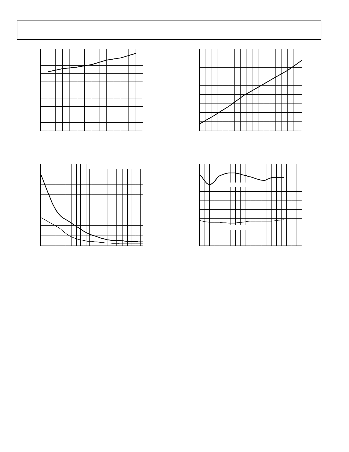
ADM823/ADM824/ADM825
2.0
1.8
1.6
1.4
1.2
1.0
0.8
0.6
TIMEOUT PERIOD (s)
0.4
0.2
0
TEMPERATURE (°C)
Figure 11. Watchdog Timeout Period vs. Temperature
160
140
120
100
MAXIMUM TRANSIENT DURATION (µs)
VTH = 4.63V
80
60
40
20
VTH = 2.93V
0
Figure 12. Maximum V
(ADM823/ADM824)
RESET OCCURS ABOVE GRAPH
OVERDRIVE VOD (mV)
Transient Duration vs. Reset Threshold Overdrive
CC
190
180
170
160
150
140
130
120
MR MINIMUM PULSE WIDTH (ns)
110
125–40 60 85250–20
04534-0-011
100
TEMPERATURE (°C)
100–50 0 50
04534-0-013
Figure 13. Manual Reset Minimum Pulse Width vs. Temperature
(ADM823/ADM825)
3.8
3.6
3.4
3.2
3.0
2.8
2.6
2.4
MINIMUM PULSE WIDTH (ns)
2.2
100010 100
04534-0-012
2.0
NEGATIVE PULSE
POSITIVE PULSE
TEMPERATURE (°C)
160–40 10 11060
04534-0-014
Figure 14. Watchdog Input Minimum Pulse Width vs. Temperature
(ADM823/ADM824)
Rev. 0 | Page 8 of 12
ADM823/ADM824/ADM825
CIRCUIT DESCRIPTION
The ADM823/ADM824/ADM825 provide microprocessor
supply voltage supervision by controlling the microprocessor’s
reset input. Code-execution errors are avoided during powerup, power-down, and brownout conditions by asserting a reset
signal when the supply voltage is below a preset threshold. They
are also avoided by allowing supply voltage stabilization with a
fixed-timeout reset pulse after the supply voltage rises above the
threshold. In addition, problems with microprocessor code
execution can be monitored and corrected with a watchdog
timer (ADM823/ ADM824). By including watchdog strobe
instructions in microprocessor code, a watchdog timer can detect
if the microprocessor code breaks down or becomes stuck in an
infinite loop. If this happens, the watchdog timer asserts a reset
pulse that restarts the microprocessor in a known state. If the
user detects a problem with the system’s operation, a manual
reset input is available (ADM823/ADM825) to reset the
microprocessor with an external push-button, for example.
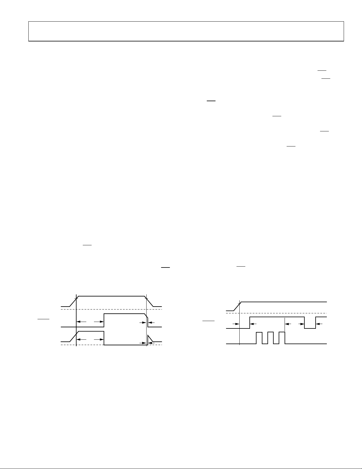
RESET OUTPUT
The ADM823 features an active-low, push-pull reset output
while the ADM824/ADM825 feature dual active-low and
active-high push-pull reset outputs. For active-low and activehigh outputs, the reset signal is guaranteed to be logic low and
logic high, respectively, for V
The reset output is asserted when V
threshold (V
), when MR is driven low, or when WDI is not
TH
serviced within the watchdog timeout period (t
remains asserted for the duration of the reset active timeout
period (t
) after VCC rises above the reset threshold, after MR
RP
transitions from low-to-high, or after the watchdog timer times
out. Figure 15 illustrates the behavior of the reset outputs.
V
V
RESET
RESET
CC
CC
1V
0V
V
CC
0V
V
CC
1V
0V
V
TH
Figure 15. Reset Timing Diagram
CC
t
RP
t
RP
down to 1 V.
is below the reset
CC
t
RD
). Reset
WD
V
TH
t
RD
04534-0-018
MANUAL RESET INPUT
The ADM823/ADM825 feature a manual reset input (MR)
which, when driven low, asserts the reset output. When
MR
transitions from low to high, reset remains asserted for the
duration of the reset active timeout period before deasserting.
The
input has a 52 kV internal pull-up so that the input is
MR
always high when unconnected. An external push-button
switch can be connected between
and ground so that the
MR
user can generate a reset. Debounce circuitry for this purpose is
integrated on-chip. Noise immunity is provided on the
MR
input and fast, negative-going transients of up to 100 ns (typ)
are ignored. A 0.1 µF capacitor between
and ground
MR
provides additional noise immunity.
WATCHDOG INPUT
The ADM823/ADM824 feature a watchdog timer which
monitors microprocessor activity. A timer circuit is cleared with
every low-to-high or high-to-low logic transition on the watchdog input pin (WDI), which detects pulses as short as 50 ns. If
the timer counts through the preset watchdog timeout period
), reset is asserted. The microprocessor is required to toggle
(t
WD
the WDI pin to avoid being reset. Failure of the microprocessor
to toggle WDI within the timeout period therefore indicates a
code execution error, and the reset pulse generated restarts the
microprocessor in a known state.
In addition to logic transitions on WDI, the watchdog timer is
also cleared by a reset assertion due to an undervoltage condition on V
the watchdog timer is cleared and does not begin counting
again until reset deassserts. The watchdog timer can be disabled
by leaving WDI floating or by three-stating the WDI driver.
RESET
or by MR being pulled low. When reset is asserted,
CC
V
WDI
V
CC
CC
1V
0V
V
CC
0V
V
CC
0V
V
TH
t
RP
Figure 16. Watchdog Timing Diagram
t
WD
t
RD
04534-0-021
Rev. 0 | Page 9 of 12
ADM823/ADM824/ADM825
APPLICATION INFORMATION
WATCHDOG INPUT CURRENT
In order to minimize watchdog input current (and minimize
overall power consumption), leave WDI low for the majority of
the watchdog timeout period. When driven high, WDI can
draw as much as 160 µA. Pulsing WDI low-high-low at a low
duty cycle reduces the effect of the large input current. When
WDI is unconnected, a window comparator disconnects the
watchdog timer from the reset output circuitry so that reset is
not asserted when the watchdog timer times out.
NEGATIVE-GOING VCC TRANSIENTS
To avoid unnecessary resets caused by fast power supply
transients, the ADM823/ADM824/ADM825 are equipped with
glitch rejection circuitry. The typical performance characteristic
in Figure 12 plots V
nitude. The curves show combinations of transient magnitude
and duration for which a reset is not generated for 4.63 V and
2.93 V reset threshold parts. For example, with the 2.93 V
threshold, a transient that goes 100 mV below the threshold and
lasts 8 µs typically does not cause a reset, but if the transient is
any bigger in magnitude or duration, a reset is generated. An
optional 0.1 µF bypass capacitor mounted close to V
additional glitch rejection.
ENSURING RESET VALID TO VCC = 0 V
Both active-low and active-high reset outputs are guaranteed to
be valid for V
resistor with push-pull configured reset outputs, valid outputs
for V
CC
output, a resistor connected between
the output low when it is unable to sink current. For the activehigh case, a resistor connected between RESET and V
the output high when it is unable to source current. A large
resistance such as 100 kΩ should be used so that it does not
overload the reset output when V
CC
as low as 0 V are possible. For an active-low reset
V
CC
transient duration vs. the transient mag-
CC
provides
CC
as low as 1 V. However, by using an external
and ground pulls
RESET
pulls
CC
is above 1 V.
CC
V
CC
WATCHDOG SOFTWARE CONSIDERATIONS
In implementing the microprocessor’s watchdog strobe code,
quickly switching WDI low-high and then high-low (minimizing
WDI high time) is desirable for current consumption reasons.
However, a more effective way of using the watchdog function
can be considered.
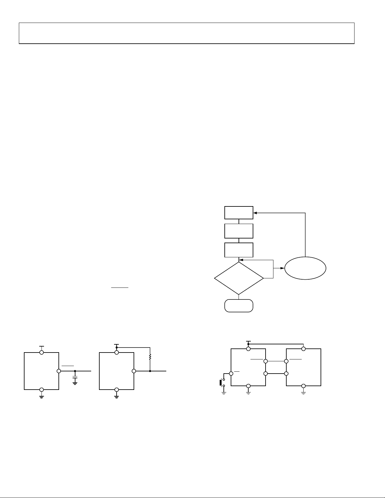
A low-high-low WDI pulse within a given subroutine prevents
the watchdog timing out. However, if the subroutine becomes
stuck in an infinite loop, the watchdog cannot detect this because
the subroutine continues to toggle WDI. A more effective coding
scheme for detecting this error involves using a slightly longer
watchdog timeout. In the program that calls the subroutine,
WDI is set high. The subroutine sets WDI low when it is called.
If the program executes without error, WDI is toggled high and
low with every loop of the program. If the subroutine enters an
infinite loop, WDI is kept low, the watchdog times out, and the
microprocessor is reset.
START
SET WDI
HIGH
PROGRAM
CODE
SUBROUTINE
SET WDI
LOW
RETURN
Figure 18. Watchdog Flow Diagram
V
CC
RESET
INFINITE LOOP:
WATCHDOG
TIMES OUT
04534-0-020
ADM823/
ADM824/
ADM825
RESET
100kΩ
Figure 17. Ensuring Reset Valid to V
ADM824/
ADM825
= 0 V
CC
RESET
100kΩ
04534-0-017
Rev. 0 | Page 10 of 12
RESET RESET
ADM823
WDI I/OMR
Figure 19. Typical Application Circuit
µP
04534-0-019

ADM823/ADM824/ADM825
Y
OUTLINE DIMENSIONS
2.00 BSC
0.30
0.15
4
3
0.65 BSC
2.10 BSC
1.10 MAX
SEATING
PLANE
0.22
0.08
1.25 BSC
1.00
0.90
0.70
0
.
1
0
5
12
PIN 1
A
M
X
0.10 COPLANARIT
COMPLIANT TO JEDEC STANDARDS MO-203AA
Figure 20. 5-Lead Plastic Surface-Mount Package [SC-70]
(KS-5)
Dimensions shown in millimeters
2.90 BSC
4 5
0.50
0.30
3
2.80 BSC
0.95 BSC
1.45 MAX
SEATING
PLANE
0.22
0.08
1.60 BSC
1.30
1.15
0.90
0.15MAX
1
2
PIN 1
1.90
BSC
COMPLIANT TO JEDEC STANDARDS MO-178AA
Figure 21. 5-Lead Small Outline Transistor Package [SOT-23]
(RJ-5)
Dimensions shown in millimeters
8°
4°
0°
0.46
0.36
0.26
10°
5°
0°
0.60
0.45
0.30
ORDERING GUIDES
Table 5. ADM823 Ordering Guide
Model Reset Threshold (V) Temperature Range Quantity Package Type Branding
ADM823LYKS-R7 4.63 –40°C to +125°C 3k SC70-5 N07
ADM823LYRJ-R7 4.63 –40°C to +125°C 3k SOT-23-5 N07
ADM823MYKS-R7 4.38 –40°C to +125°C 3k SC70-5 N07
ADM823MYRJ-R7 4.38 –40°C to +125°C 3k SOT-23-5 N07
ADM823TYKS-R7 3.08 –40°C to +125°C 3k SC70-5 N07
ADM823TYRJ-R7 3.08 –40°C to +125°C 3k SOT-23-5 N07
ADM823SYKS-R7 2.93 –40°C to +125°C 3k SC70-5 N07
ADM823SYRJ-R7 2.93 –40°C to +125°C 3k SOT-23-5 N07
ADM823RYKS-R7 2.63 –40°C to +125°C 3k SC70-5 N07
ADM823RYRJ-R7 2.63 –40°C to +125°C 3k SOT-23-5 N07
ADM823ZYKS-R7 2.32 –40°C to +125°C 3k SC70-5 N07
ADM823YYKS-R7 2.19 –40°C to +125°C 3k SC70-5 N07
Rev. 0 | Page 11 of 12

ADM823/ADM824/ADM825
Table 6. ADM824 Ordering Guide
1
Model
ADM824LYKS-R7 4.63 –40°C to +125°C 3k SC70-5 N08
ADM824LYRJ-R7 4.63 –40°C to +125°C 3k SOT-23-5 N08
ADM824MYKS-R7 4.38 –40°C to +125°C 3k SC70-5 N08
ADM824MYRJ-R7 4.38 –40°C to +125°C 3k SOT-23-5 N08
ADM824TYKS-R7 3.08 –40°C to +125°C 3k SC70-5 N08
ADM824TYRJ-R7 3.08 –40°C to +125°C 3k SOT-23-5 N08
ADM824SYKS-R7 2.93 –40°C to +125°C 3k SC70-5 N08
ADM824SYRJ-R7 2.93 –40°C to +125°C 3k SOT-23-5 N08
ADM824RYKS-R7 2.63 –40°C to +125°C 3k SC70-5 N08
ADM824RYRJ-R7 2.63 –40°C to +125°C 3k SOT-23-5 N08
ADM824ZYKS-R7 2.32 –40°C to +125°C 3k SC70-5 N08
ADM824YYKS-R7 2.19 –40°C to +125°C 3k SC70-5 N08
1
All of the ADM824 models are nonstandard. For availability of alternate versions, contact Sales.
Table 7. ADM825 Ordering Guide
Model Reset Threshold (V) Temperature Range Quantity Package Type Branding
ADM825LYKS-R7 4.63 –40°C to +125°C 3k SC70-5 N09
ADM825LYRJ-R7 4.63 –40°C to +125°C 3k SOT-23-5 N09
ADM825MYKS-R7 4.38 –40°C to +125°C 3k SC70-5 N09
ADM825MYRJ-R7 4.38 –40°C to +125°C 3k SOT-23-5 N09
ADM825TYKS-R7 3.08 –40°C to +125°C 3k SC70-5 N09
ADM825TYRJ-R7 3.08 –40°C to +125°C 3k SOT-23-5 N09
ADM825SYKS-R7 2.93 –40°C to +125°C 3k SC70-5 N09
ADM825SYRJ-R7 2.93 –40°C to +125°C 3k SOT-23-5 N09
ADM825RYKS-R7 2.63 –40°C to +125°C 3k SC70-5 N09
ADM825RYRJ-R7 2.63 –40°C to +125°C 3k SOT-23-5 N09
ADM825ZYKS-R7 2.32 –40°C to +125°C 3k SC70-5 N09
ADM825YYKS-R7 2.19 –40°C to +125°C 3k SC70-5 N09
Reset Threshold (V) Temperature Range Quantity Package Type Branding
© 2004 Analog Devices, Inc. All rights reserved. Trademarks and
registered trademarks are the property of their respective owners.
D04534–0–10/04(0)
Rev. 0 | Page 12 of 12
 Loading...