

Microprocessor Supervisory
V
FEATURES
Superior upgrade for MAX811/MAX812
Specified over temperature
Low power consumption: 5 μA typical
Precision voltage monitor: 2.5 V, 3 V, 3.3 V, 5 V options
Reset assertion down to 1 V
Power-on reset: 140 ms minimum
Logic low
RESET
output (ADM811)
Logic high RESET output (ADM812)
Built-in manual reset
APPLICATIONS
Microprocessor systems
Controllers
Intelligent instruments
Automotive systems
Safety systems
Portable instruments
CC
Circuit in 4-Lead SOT-143 with DSP
ADM811/ADM812
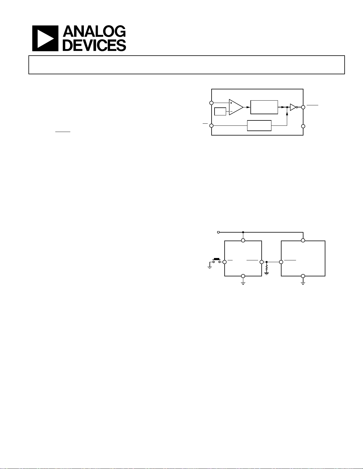
FUNCTIONAL BLOCK DIAGRAM
ADM811/ADM812
CC
V
REF
MR
RESET
GENERATOR
DEBOUNCE
Figure 1.
RESET/RESE T
GND
0092-001
GENERAL DESCRIPTION
The ADM811/ADM812 are reliable voltage monitoring devices
suitable for use in most voltage monitoring applications. The
ADM811/ADM812 are designed to monitor six different
voltages, each allowing a 5% or 10% degradation of standard
PSU voltages before a reset occurs. These voltages have been
selected for the effective monitoring of 2.5 V, 3 V, 3.3 V, and 5 V
supply voltage levels.
Included in this circuit is a debounced manual reset input.
Reset can be activated using an electrical switch (or an input
from another digital device) or by a degradation of the supply
voltage. The manual reset function is very useful, especially if
the circuit in which the ADM811/ADM812 are operating enters
into a state that can only be detected by the user. Allowing the
user to reset a system manually can reduce the damage or
danger that could otherwise be caused by an out-of-control
or locked system.
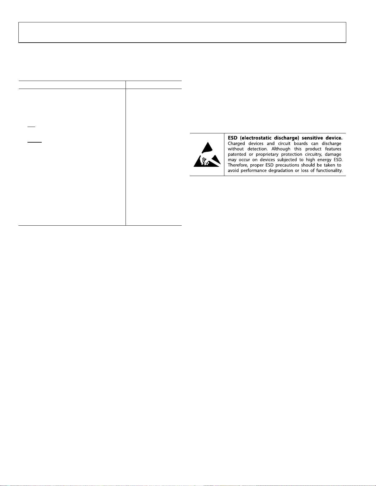
V
CC
ADM811
MR RESET
GND
Figure 2. Typical ADM811 Operating Circuit
100kΩ
V
CC
MICROPROCESSOR
SYSTEM
RESET
GND
0092-002
Rev. F
Information furnished by Analog Devices is believed to be accurate and reliable. However, no
responsibility is assumed by Analog Devices for its use, nor for any infringements of patents or other
rights of third parties that may result from its use. Specifications subject to change without notice. No
license is granted by implication or otherwise under any patent or patent rights of Analog Devices.
Trademarks and registered trademarks are the property of their respective owners.
One Technology Way, P.O. Box 9106, Norwood, MA 02062-9106, U.S.A.
Tel: 781.329.4700 www.analog.com
Fax: 781.461.3113 ©2009 Analog Devices, Inc. All rights reserved.

ADM811/ADM812
TABLE OF CONTENTS
Features .............................................................................................. 1
Applications ....................................................................................... 1
Functional Block Diagram .............................................................. 1
General Description ......................................................................... 1
Revision History ............................................................................... 2
Specifications ..................................................................................... 3
Absolute Maximum Ratings ............................................................ 4
ESD Caution .................................................................................. 4
Pin Configuration and Function Descriptions ............................. 5
Typical Performance Characteristics ............................................. 6
Circuit Information .......................................................................... 7
REVISION HISTORY
8/09—Rev. E to Rev. F
Changes to Ordering Guide .......................................................... 10
5/08—Rev. D to Rev. E
Changes to Table 2 ............................................................................ 4
Changes to Outline Dimensions ..................................................... 9
Changes to Ordering Guide .......................................................... 10
5/06—Rev. C to Rev. D
Changes to Ordering Guide ............................................................ 9
2/03—Rev. B to Rev. C
Changes Features .............................................................................. 1
Changes to General Description .................................................... 1
Changes to Specifications ................................................................ 2
Removed Note 2 from Ordering Guide ......................................... 3
Reset Thresholds ...........................................................................7
Reset Output ..................................................................................7
Manual Reset ..................................................................................7
Glitch Immunity ............................................................................7
Interfacing to Other Devices ............................................................8
Output .............................................................................................8
Benefits of a Very Accurate Reset Threshold ............................8
Ensuring a Valid
Outline Dimensions ..........................................................................9
Ordering Guide .......................................................................... 10
Changes to Pin Function Descriptions ........................................... 4
Removed Note from Table I ............................................................ 6
1/03—Rev. A to Rev. B
Added ADM812 ................................................................. Universal
Changes to Specifications ................................................................. 2
Changes to Ordering Guide ............................................................. 3
Changes to Pin Configuration ......................................................... 4
Changes to Pin Function Description ............................................ 4
Additions to Table I ........................................................................... 6
Changes to Manual Reset section .................................................... 6
5/02—Rev. 0 to Rev. A
Deletion of ADM812.......................................................... Universal
RESET
/Reset Output Down to VCC = 0 V....8
Rev. F | Page 2 of 12

ADM811/ADM812
SPECIFICATIONS
VCC = full operating range; TA = T
models, unless otherwise noted.
Table 1.
Parameter Min Typ Max Unit Test Conditions/Comments
SUPPLY
Voltage 1.0 5.5 V TA = 0°C to 70°C
1.2 V TA = −40°C to +85°C
Current 8 15 μA VCC < 5.5 V, ADM81xL/M, I
5 10 μA VCC < 3.6 V, ADM81xR/S/T/Z, I
RESET VOLTAGE THRESHOLD
ADM81xL 4.54 4.63 4.72 V TA = 25°C
ADM81xL 4.50 4.75 V TA = −40°C to +85°C
ADM81xM 4.30 4.38 4.46 V TA = 25°C
ADM81xM 4.25 4.50 V TA = −40°C to +85°C
ADM81xT 3.03 3.08 3.14 V TA = 25°C
ADM81xT 3.00 3.15 V TA = −40°C to +85°C
ADM81xS 2.88 2.93 2.98 V TA = 25°C
ADM81xS 2.85 3.00 V TA = −40°C to +85°C
ADM81xR 2.58 2.63 2.68 V TA = 25°C
ADM81xR 2.55 2.70 V TA = −40°C to +85°C
ADM81xZ 2.28 2.32 2.35 V TA = 25°C
ADM81xZ 2.25 2.38 V TA = −40°C to +85°C
RESET THRESHOLD TEMPERATURE COEFFICIENT 30 ppm/°C
VCC TO RESET/RESET DELAY
20 μs VOD = 125 mV, ADM81xR/S/T/Z
RESET ACTIVE TIMEOUT PERIOD 140 560 ms VCC = V
300 700 ms ADM811-3T only
MANUAL RESET
Minimum Pulse Width 10 μs
Glitch Immunity 100 ns
RESET/RESET Propagation Delay
Pull-Up Resistance 10 20 30 kΩ
The Manual Reset Circuit Acts On
An Input Rising Above 2.3 V VCC > V
An Input Falling Below 0.8 V VCC > V
An Input Rising Above 0.7 × VCC V VCC > V
An Input Falling Below
RESET/RESET Output Voltage
Low (ADM812R/S/T/Z) 0.3 V VCC = V
Low (ADM812L/M) 0.4 V VCC = V
High (ADM812R/S/T/Z/L/M) 0.8 × VCC V 1.8 V < VCC < V
Low (ADM811R/S/T/Z) 0.3 V VCC = V
Low (ADM811L/M) 0.4 V VCC = V
Low (ADM811R/S/T/Z/L/M) 0.3 V VCC > 1.0 V, I
High (ADM811R/S/T/Z) 0.8 × VCC V VCC > V
High (ADM811L/M) VCC × 1.5 V VCC > V
MIN
to T
; VCC typical = 5 V for L/M models, 3.3 V for T/S models, 3 V for R model, 2.5 V for Z
MAX
OUT
40 μs V
= 125 mV, ADM81xL/M
OD
TH(MAX)
0.5 μs
, ADM81xL/M
TH(MAX)
, ADM81xL/M
TH(MAX)
, ADM81xR/S/T/Z
0.25 × VCC V VCC > V
TH(MAX)
, ADM81xR/S/T/Z
TH(MAX)
, I
SINK
, I
SINK
TH(MIN)
, I
SINK
= 50 μA
SINK
, I
SOURCE
, I
SOURCE
= 1.2 mA
= 3.2 mA
, I
SOURCE
= 1.2 mA
= 3.2 mA
= 500 μA
= 800 μA
TH(MAX)
TH(MAX)
TH(MIN), ISINK
TH(MIN)
TH(MAX)
TH(MAX)
= 0 mA
= 0 mA
OUT
= 150 μA
Rev. F | Page 3 of 12
ADM811/ADM812
ABSOLUTE MAXIMUM RATINGS
Typical values are at TA = 25°C, unless otherwise noted.
Table 2.
Parameter Rating
Terminal Voltage (With Respect to Ground)
V
−0.3 V to +6 V
CC
All Other Inputs −0.3 V to VCC + 0.3 V
Input Current
VCC 20 mA
MR
Output Current
RESET
Power Dissipation (TA = 70°C)
RA-4 (SOT-143) 200 mW
Derate by 4 mW/°C Above 70°C
θJA Thermal Impedance
Operating Temperature Range −40°C to +85°C
Storage Temperature Range −65°C to +160°C
Lead Temperature (Soldering, 10 sec) 300°C
Vapor Phase (60 sec) 215°C
Infrared (15 sec) 220°C
ESD Rating 3 kV
20 mA
20 mA
330°C/W
Stresses above those listed under Absolute Maximum Ratings
may cause permanent damage to the device. This is a stress
rating only; functional operation of the device at these or any
other conditions above those indicated in the operational
section of this specification is not implied. Exposure to absolute
maximum rating conditions for extended periods may affect
device reliability.
ESD CAUTION
Rev. F | Page 4 of 12
ADM811/ADM812
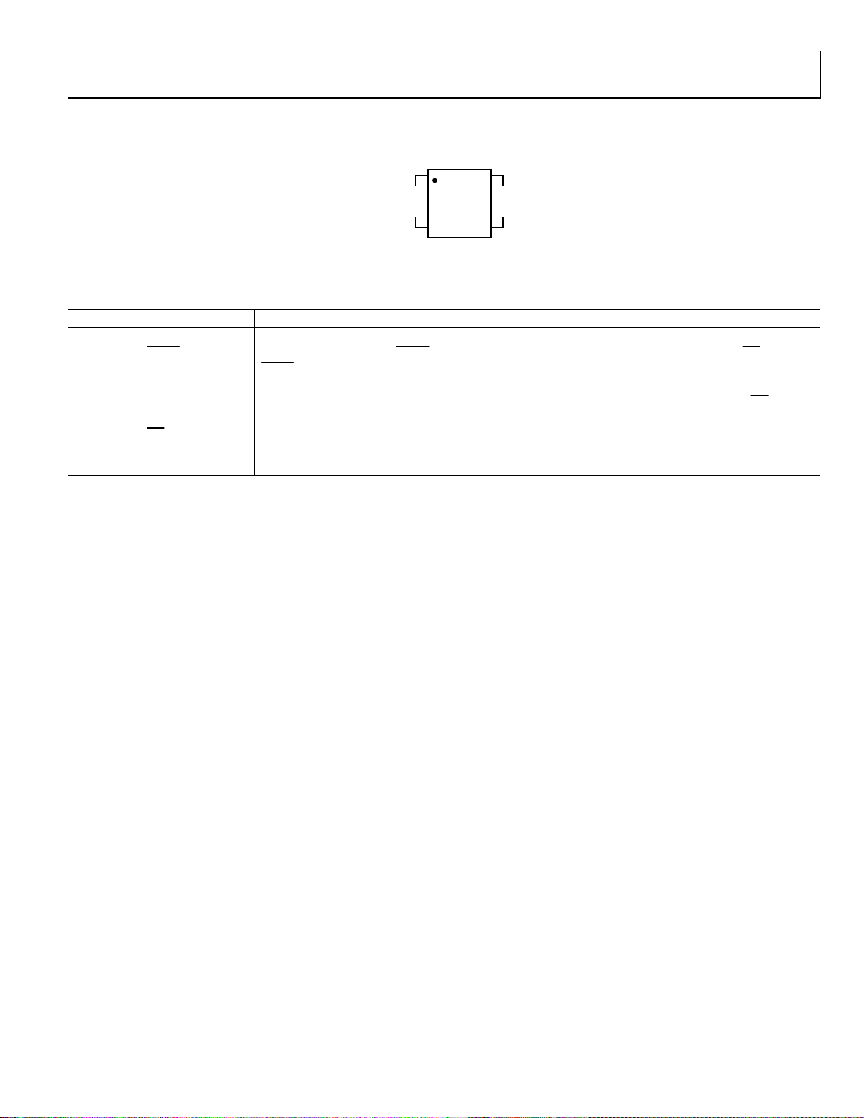
PIN CONFIGURATION AND FUNCTION DESCRIPTIONS
GND
1
ADM811/
ADM812
RESET/RESET
Figure 3. Pin Configuration
TOP VIEW
2
(Not to Scale)
Table 3. Pin Function Descriptions
Pin No. Mnemonic Description
1 GND Ground Reference For All Signals, 0 V.
2
RESET
(ADM811)
Active Low Logic Output. RESET
then remains low for at least 140 ms (at least 300 ms for the ADM811-3T) after VCC rises above the
RESET
remains low while VCC is below the reset threshold or when MR is low;
reset threshold.
RESET (ADM812)
Active High Logic Output. RESET remains high while V
RESET then remains high for 240 ms (typical) after VCC rises above the reset threshold.
3
MR
Manual Reset. This active low debounced input ignores input pulses of 100 ns or less (typical) and is
guaranteed to accept input pulses of greater than 10 μs. Leave floating when not used.
4 VCC Monitored Supply Voltage of 2.5 V, 3 V, 3.3 V, or 5 V.
V
4
CC
MR
3
00092-003
is below the reset threshold or when MR is low;
CC
Rev. F | Page 5 of 12

ADM811/ADM812
TYPICAL PERFORMANCE CHARACTERISTICS
12
IDD @ VCC = 5.5V
10
8
6
(µA)
DD
I
4
2
0
–40 –20 0 20 30 50 70 85 100 120
@ VCC = 3V
I
DD
@ VCC = 1V
I
DD
TEMPERATURE (° C)
00092-004
Figure 4. Supply Current vs. Temperature (ADM81xR/S/T/Z) Figure 7. Supply Current vs. Temperature (ADM81xL/M)
1000
900
800
700
600
500
400
300
200
V
POWER-DOW N RESET DEL AY (µs)
100
0
–40 –20 0 20 30 50 70 85 100 120
Figure 5. Power-Down
= 125mV
OD
VOD = 20mV
V
= 200mV
OD
RESET
TEMPERATURE ( °C)
00092-005
Delay vs. Temperature (ADM81xR/S/T/Z) Figure 8. Power-Down
299
294
279
274
269
264
259
254
POWER-UP RE SET TIM EOUT (ms)
249
244
–40 –20 0 20 30 50 70 85 100 120
ADM81xL/M
ADM81xR/S/T/Z
TEMPERATURE (° C)
00092-006
Figure 6. Power-Up RESET Timeout vs. Temperature
10
9
8
7
6
5
(µA)
DD
I
4
3
2
1
0
–40 –20 0 20 30 50 70 85 100 120
900
800
700
600
500
400
300
200
POWER-DOW N RESET DEL AY (µs)
1.007
1.006
1.005
1.004
1.003
1.002
1.002
1.001
1.000
0.999
0.998
NORMALIZE D RESET THRESHOLD
0.997
0.996
0.995
100
0
V
OD
= 200mV
V
OD
–40 –20 0 20 30 50 70 85 100 120
–40 –20 0 20 30 50 70 85 100 120
IDD @ VCC = 5.5V
TEMPERATURE (° C)
VOD = 20mV
= 125mV
TEMPERATURE (° C)
RESET
I
@ VCC = 3V
DD
@ VCC = 1V
I
DD
Delay vs. Temperature (ADM81xL/M)
TEMPERATURE (° C)
Figure 9. RESET Threshold Deviation vs. Temperature
00092-007
00092-008
00092-009
Rev. F | Page 6 of 12
ADM811/ADM812
CIRCUIT INFORMATION
RESET THRESHOLDS
A reset output is provided to the microprocessor whenever the
input is below the reset threshold. The actual reset threshold
V
CC
depends on whether an L, M, T, S, R, or Z suffix is used (see
Tabl e 4).
Table 4. Reset Threshold Options
Model Reset Threshold (V)
ADM811LART 4.63
ADM811MART 4.38
ADM811TART 3.08
ADM811-3TART 3.08
ADM811SART 2.93
ADM811RART 2.63
ADM811ZART 2.32
ADM812LART 4.63
ADM812MART 4.38
ADM812TART 3.08
ADM812SART 2.93
ADM812RART 2.63
ADM812ZART 2.32
RESET OUTPUT
On power-up and after VCC rises above the reset threshold, an
internal timer holds the reset output active for 240 ms (typical).
This is intended as a power-on reset signal for the processor. It
allows time for both the power supply and the microprocessor
to stabilize after power-up. If a power supply brownout or
interruption occurs, the reset output is similarly activated and
remains active for 240 ms (typical) after the supply recovers.
This allows time for the power supply and microprocessor to
stabilize.
The ADM811 provides an active low reset output (
RESET
)
while the ADM812 provides an active high output (RESET).
RESET
During power-down of the ADM811, the
remains valid (low) with V
as low as 1 V. This ensures that
CC
output
the microprocessor is held in a stable shutdown condition as
the supply falls and also ensures that no spurious activity can
occur via the microprocessor as it powers up.
MANUAL RESET
The ADM811/ADM812 are equipped with a manual reset
input. This input is designed to operate in a noisy environment
where unwanted glitches could be induced. These glitches could
be produced by the bouncing action of a switch contact, or where a
manual reset switch may be located some distance away from
the circuit (the cabling of which can pick up noise).
The manual reset input is guaranteed to ignore logically valid
inputs that are faster than 100 ns and to accept inputs longer in
duration than 10 μs.
GLITCH IMMUNITY
The ADM811/ADM812 contain internal filtering circuitry
providing glitch immunity from fast transient glitches on the
power supply line.
V
RESET
V
CC
t
= RESET TI ME = 250ms TYPICAL
1
V
= RESET VOLTAGE THRESHOLD
REF
V
REF
REF
t
1
Figure 10. Power Fall
V
REF
RESET
t
1
Timing
V
REF
00092-010
Rev. F | Page 7 of 12

ADM811/ADM812
V
INTERFACING TO OTHER DEVICES
OUTPUT
The ADM811/ADM812 are designed to integrate with as many
devices as possible. One feature of the ADM811/ADM812 is the
reset output, which is directly proportional to V
anteed only while V
is greater than 1 V). This enables the part
CC
(this is guar-
CC
to be used with both 3 V and 5 V, or any nominal voltage within
the minimum and maximum specifications for V
.
CC
BENEFITS OF A VERY ACCURATE RESET THRESHOLD
Because the ADM811/ADM812 can operate effectively even
when there are large degradations of the supply voltages, the
possibility of a malfunction during a power failure is greatly
reduced. Another advantage of the ADM811/ADM812 is its
very accurate internal voltage reference circuit. Combined,
these benefits produce an exceptionally reliable microprocessor
supervisory circuit.
Figure 11. Ensuring a Valid
ENSURING A VALID RESET/RESET
OUTPUT DOWN TO V
When VCC falls below 0.8 V, the
ADM812 no longer sinks current. Therefore, a high impedance
CMOS logic input connected to
undetermined logic levels. To eliminate this problem, a 100 kΩ
resistor should be connected from
CC
V
CC
ADM811
RESET
GND
CC
RESET
Output Down to VCC = 0 V
= 0 V
RESET
/RESET of the ADM811/
RESET
/RESET can drift to
RESET
/RESET to ground.
0092-011
Rev. F | Page 8 of 12

ADM811/ADM812
OUTLINE DIMENSIONS
3.04
2.90
2.80
0.20
BSC
1.40
1.30
1.20
1.22
0.80
4
12
1.92 BSC
0.89
0.76
COMPLIANT TO JEDEC STANDARDS TO-253-AA
2.64
3
2.10
1.07
0.90
0.75
0.20
0.08
0.54 REF
0.50
0.30
0.100
0.013
SEATING
PLANE
Figure 12. 4-Lead Small Outline Transistor Package [SOT-143]
(RA-4)
Dimensions shown in millimeters
0.60
0.50
0.40
8°
0°
073105-A
Rev. F | Page 9 of 12

ADM811/ADM812
ORDERING GUIDE
Reset
Threshold (V)
Model
1
ADM811LART-REEL 4.63 –40°C to +85°C 10,000 4-Lead SOT-143 RA-4 MBV
ADM811LART-REEL7 4.63 –40°C to +85°C 3,000 4-Lead SOT-143 RA-4 MBV
ADM811LARTZ-REEL
ADM811LARTZ-REEL7
2
4.63 –40°C to +85°C 10,000 4-Lead SOT-143 RA-4 M4J
2
4.63 –40°C to +85°C 3,000 4-Lead SOT-143 RA-4 M4J
ADM811MART-REEL7 4.38 –40°C to +85°C 3,000 4-Lead SOT-143 RA-4 MBT
2
ADM811MARTZ-REEL
ADM811MARTZ-REEL7
4.38 –40°C to +85°C 10,000 4-Lead SOT-143 RA-4 MBT #
2
4.38 –40°C to +85°C 3,000 4-Lead SOT-143 RA-4 MBT #
ADM811TART-REEL 3.08 –40°C to +85°C 10,000 4-Lead SOT-143 RA-4 MBG
ADM811TART-REEL7 3.08 –40°C to +85°C 3,000 4-Lead SOT-143 RA-4 MBG
ADM811TARTZ-REEL
ADM811TARTZ-REEL7
2
3.08 –40°C to +85°C 10,000 4-Lead SOT-143 RA-4 MBG #
2
3.08 –40°C to +85°C 3,000 4-Lead SOT-143 RA-4 MBG #
ADM811-3TART-REEL7 3.08 –40°C to +85°C 3,000 4-Lead SOT-143 RA-4 MB3
ADM811-3TARTZ-RL
ADM811-3TARTZ-RL7
2
3.08 –40°C to +85°C 10,000 4-Lead SOT-143 RA-4 M4E
2
3.08 –40°C to +85°C 3,000 4-Lead SOT-143 RA-4 M4E
ADM811SART-REEL 2.93 –40°C to +85°C 10,000 4-Lead SOT-143 RA-4 MBE
ADM811SART-REEL7 2.93 –40°C to +85°C 3,000 4-Lead SOT-143 RA-4 MBE
2
ADM811SARTZ-REEL
ADM811SARTZ-REEL7
2.93 –40°C to +85°C 10,000 4-Lead SOT-143 RA-4 MBE #
2
2.93 –40°C to +85°C 3,000 4-Lead SOT-143 RA-4 MBE #
ADM811RART-REEL7 2.63 –40°C to +85°C 3,000 4-Lead SOT-143 RA-4 MBB
2
ADM811RARTZ-REEL
ADM811RARTZ-REEL7
2.63 –40°C to +85°C 10,000 4-Lead SOT-143 RA-4 M4N
2
2.63 –40°C to +85°C 3,000 4-Lead SOT-143 RA-4 M4N
ADM811ZART-REEL 2.32 –40°C to +85°C 10,000 4-Lead SOT-143 RA-4 MBZ
ADM811ZART-REEL7 2.32 –40°C to +85°C 3,000 4-Lead SOT-143 RA-4 MBZ
2
ADM811ZARTZ-REEL
ADM811ZARTZ-REEL7
2.32 –40°C to +85°C 10,000 4-Lead SOT-143 RA-4 M6G
2
2.32 –40°C to +85°C 3,000 4-Lead SOT-143 RA-4 M6G
ADM812LART-REEL 4.63 –40°C to +85°C 10,000 4-Lead SOT-143 RA-4 MCV
ADM812LART-REEL7 4.63 –40°C to +85°C 3,000 4-Lead SOT-143 RA-4 MCV
2
ADM812LARTZ-REEL
ADM812LARTZ-REEL7
4.63 –40°C to +85°C 10,000 4-Lead SOT-143 RA-4 M5D
2
4.63 –40°C to +85°C 3,000 4-Lead SOT-143 RA-4 M5D
ADM812MART-REEL 4.38 –40°C to +85°C 10,000 4-Lead SOT-143 RA-4 MCT
ADM812MART-REEL7 4.38 –40°C to +85°C 3,000 4-Lead SOT-143 RA-4 MCT
2
ADM812MARTZ-REEL
ADM812MARTZ-REEL7
4.38 –40°C to +85°C 10,000 4-Lead SOT-143 RA-4 M6D
2
4.38 –40°C to +85°C 3,000 4-Lead SOT-143 RA-4 M6D
ADM812TART-REEL7 3.08 –40°C to +85°C 3,000 4-Lead SOT-143 RA-4 MCG
ADM812TARTZ-REEL
ADM812TARTZ-REEL7
2
3.08 –40°C to +85°C 10,000 4-Lead SOT-143 RA-4 M68
2
3.08 –40°C to +85°C 3,000 4-Lead SOT-143 RA-4 M68
ADM812SART-REEL 2.93 –40°C to +85°C 10,000 4-Lead SOT-143 RA-4 MCE
ADM812SART-REEL7 2.93 –40°C to +85°C 3,000 4-Lead SOT-143 RA-4 MCE
2
ADM812SARTZ-REEL
ADM812SARTZ-REEL7
2.93 –40°C to +85°C 10,000 4-Lead SOT-143 RA-4 M67
2
2.93 –40°C to +85°C 3,000 4-Lead SOT-143 RA-4 M67
ADM812RART-REEL 2.63 –40°C to +85°C 10,000 4-Lead SOT-143 RA-4 MCB
ADM812RART-REEL7 2.63 –40°C to +85°C 3,000 4-Lead SOT-143 RA-4 MCB
2
ADM812RARTZ-REEL
ADM812RARTZ-REEL7
2.63 –40°C to +85°C 10,000 4-Lead SOT-143 RA-4 M6F
2
2.63 –40°C to +85°C 3,000 4-Lead SOT-143 RA-4 M6F
ADM812ZART-REEL 2.32 –40°C to +85°C 10,000 4-Lead SOT-143 RA-4 MCZ
ADM812ZART-REEL7 2.32 –40°C to +85°C 3,000 4-Lead SOT-143 RA-4 MCZ
ADM812ZARTZ-REEL
ADM812ZARTZ-REEL7
1
Available only in reels.
2
Z = RoHS Compliant Part. RoHS-compliant parts may have # branded on either the top or bottom of the device.
2
2.32 –40°C to +85°C 10,000 4-Lead SOT-143 RA-4 M69
2
2.32 –40°C to +85°C 3,000 4-Lead SOT-143 RA-4 M69
Te mp e ra tu r e
Range
Ordering
Quantity
Package
Description
Package
Option Branding
Rev. F | Page 10 of 12

ADM811/ADM812
NOTES
Rev. F | Page 11 of 12

ADM811/ADM812
NOTES
©2009 Analog Devices, Inc. All rights reserved. Trademarks and
registered trademarks are the property of their respective owners.
D00092-0-8/09(F)
Rev. F | Page 12 of 12
 Loading...