Low Voltage, High Accuracy, Triple/Quad
V
www.BDTIC.com/ADI
Voltage Microprocessor Supervisory Circuit
FEATURES
Accurate monitoring of up to four power supply voltages
5 factory-set threshold options: 1.8 V, 2.5 V, 3.0 V, 3.3 V, 5 V
Adjustable input threshold voltage = 0.62 V (1.5% accuracy)
200 ms typical reset timeout
Open-drain
Reset output stage: active low, valid to IN
Low power consumption (35 μA)
Power supply glitch immunity
Specified from −40°C to +85°C
6-lead SOT-23 package
APPLICATIONS
Telecommunications
Microprocessor systems
Desktop and notebook computers
Data storage equipment
Servers/workstations
GENERAL DESCRIPTION
The ADM6710 is a low voltage, high accuracy supervisory
circuit. The device monitors up to four system supply voltages.
The ADM6710 incorporates a variety of internally pretrimmed
u
ndervoltage threshold options for monitoring 1.8 V, 2.5 V,
3.0 V, 3.3 V and 5.0 V supply voltages. The ADM6710Q offers
three adjustable thresholds for monitoring voltages down to
0.62 V. See the
o
f all available options.
If a monitored power supply voltage falls below the minimum
v
oltage threshold, a single active low output asserts, triggering a
system reset. The output is open drain with a weak internal
pull-up to the monitored IN
RESET
output (10 μA internal pull-up)
= 1 V or IN2 = 1 V
1
Ordering Guide section for a list and description
supply (or to VCC in the case of the
2
ADM6710
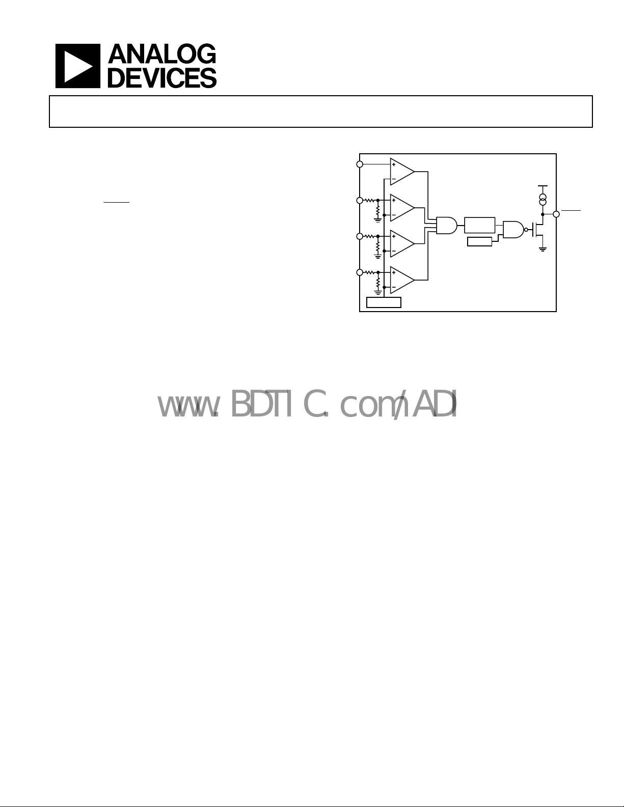
FUNCTIONAL BLOCK DIAGRAM
IN
1
IN2,
CC
IN
3
IN
4
0.62V REF
ADM6710Q) of typically 10 μA. Once all voltages rise above the
selected threshold level, the reset signal remains low for the
reset timeout period (200 ms typical).
The ADM6710 output remains valid as long as IN
exceeds 1 V, whereas for the ADM6710Q, the output remains
valid as long as V
exceeds 2 V.
CC
Unused monitored inputs should not be allowed to float or to
grounded, instead they should be connected to a supply
be
voltage greater than their specified threshold voltages.
The ADM6710 is available in a 6-lead SOT-23 package. The
de
vice operates over the extended temperature range of −40°C
to +85°C.
ADM6710
TIMEOUT
Figure 1.
200ms
UVLO
IN2, V
or IN2
1
CC
RESET
06626-001
Rev. 0
Information furnished by Analog Devices is believed to be accurate and reliable. However, no
responsibility is assumed by Anal og Devices for its use, nor for any infringements of patents or ot her
rights of third parties that may result from its use. Specifications subject to change without notice. No
license is granted by implication or otherwise under any patent or patent rights of Analog Devices.
Trademarks and registered trademarks are the property of their respective owners.
One Technology Way, P.O. Box 9106, Norwood, MA 02062-9106, U.S.A.
Tel: 781.329.4700 www.analog.com
Fax: 781.461.3113 ©2007 Analog Devices, Inc. All rights reserved.

ADM6710
www.BDTIC.com/ADI
TABLE OF CONTENTS
Features.............................................................................................. 1
Applications....................................................................................... 1
Functional Block Diagram .............................................................. 1
General Description ......................................................................... 1
Revision History ............................................................................... 2
Specifications..................................................................................... 3
Absolute Maximum Ratings............................................................ 4
ESD Caution.................................................................................. 4
Pin Configurations and Function Descriptions ........................... 5
REVISION HISTORY
6/07—Revision 0: Initial Version
Typical Performance Characteristics..............................................6
Theory of Operation .........................................................................8
Input Configuration......................................................................8
RESET
Output Configuration .....................................................8
Addition Of Manual Reset ...........................................................8
Outline Dimensions..........................................................................9
Ordering Guide .............................................................................9
Rev. 0 | Page 2 of 12

ADM6710
www.BDTIC.com/ADI
SPECIFICATIONS
V
= 1 V to 5.5 V, TA = −40°C to +85°C, unless otherwise noted. Typical values are V
IN2
Table 1.
Parameter Min Typ Max Units Test Conditions/Comments
OPERATING VOLTAGE RANGE
1
V
CC
2
V
IN2
2.0 5.5 V ADM6710Q only
1.0 5.5 V All devices except ADM6710Q; TA = 0°C to +85°C
1.2 5.5 V All devices except ADM6710Q; TA = −40°C to +85°C
INPUT CURRENT
INx Input Current
25 40 μA
IN
supplies)
55 115 μA
IN
The supply splits into 25 μA for the resistor divider and
30 μA for other circuits.
0.4 μA V
0.2 μA V
ICC Input Current
35 50 μA ADM6710Q only; VCC = 5.5 V
THRESHOLD VOLTAGE
Threshold Voltage (VTH) 4.50 4.63 4.75 V INX decreasing; 5 V (−5%)
4.25 4.38 4.50 V INX decreasing; 5 V (−10%)
3.00 3.08 3.15 V INX decreasing; 3.3 V (−5%)
2.85 2.93 3.00 V INX decreasing; 3.3 V (−10%)
2.70 2.78 2.85 V INX decreasing; 3.0 V (−5%)
2.55 2.63 2.70 V INX decreasing; 3.0 V (−10%)
2.25 2.32 2.38 V INX decreasing; 2.5 V (−5%)
2.13 2.19 2.25 V INX decreasing; 2.5 V (−10%)
1.62 1.67 1.71 V INX decreasing; 1.8 V (−5%)
1.53 1.58 1.62 V INX decreasing; 1.8 V (−10%)
Adjustable Threshold (VTH) 0.611 0.620 0.629 V INX decreasing
RESET THRESHOLD HYSTERESIS ( V
RESET THRESHOLD TEMPERATURE
COEFFICIENT (TCV
)
TH
) 0.3 %VTH INX increasing relative to INX decreasing
HYST
60 ppm/°C
INX to RESET DELAY (tRP) 30 μs VIN falling at 10 mV/μs from VTH to VTH − 50 mV
RESET TIMEOUT PERIOD (tRP) 140 200 280 ms
RESET OUTPUT LOW (VOL)
0.3 V
V
0.4 V V
RESET OUTPUT HIGH (VOH)
0.8 × V
RESET OUTPUT HIGH SOURCE
CURRENT (I
1
Note that the ADM6710Q is powered from VCC.
2
RESET
The
)
OH
output is guaranteed to be in the correct state for IN1 or IN2 down to 1 V.
0.3 V V
0.8 × V
V
CC
V
IN2
10 μA
V
V
V
= 3.0 V to 3.3 V, TA = 25°C.
IN2
= Nominal input voltage (for 1.8 V, 2.5 V and 5.0 V
X
= Nominal input voltage (for 3.0 V and 3.3 V supplies).
2
= 0 V to 0.85 V (for adjustable thresholds)
IN1
, V
= 0 V to 0.85 V (for adjustable thresholds)
IN3
IN4
, V
= 5 V, I
IN2
CC
, VCC = 2.5 V, I
IN2
= 1.0 , I
IN2
≥ 2.0 V, I
CC
≥ 2.0 V, I
IN2
≥ 2.0 V,
IN2
= 2 mA
SINK
= 1.2 mA
SINK
= 20 μA, TA = 0°C to +85°C
SINK
RESET
SOURCE
SOURCE
RESET
= 4 μA,
= 4 μA,
deasserted
deasserted (ADM6710Q only)
RESET
deasserted
Rev. 0 | Page 3 of 12

ADM6710
www.BDTIC.com/ADI
ABSOLUTE MAXIMUM RATINGS
Table 2.
Parameter Rating
RESET
VCC, INX,
Continuous
Storage Temperature Range −65°C to +125°C
Operating Temperature Range −40°C to +85°C
Lead Temperature (10 sec) 300°C
Junction Temperature 135°C
Table 3. Thermal Resistance
Package Type θJA Unit
6-lead SOT-23 169.5 °C/W
to GND
RESET
Current
−0.3 V to +6 V
20 mA
Stresses above those listed under Absolute Maximum Ratings
may cause permanent damage to the device. This is a stress
rating only and functional operation of the device at these or
any other conditions above those indicated in the operational
section of this specification is not implied. Exposure to absolute
maximum rating conditions for extended periods may affect
device reliability.
ESD CAUTION
Rev. 0 | Page 4 of 12
 Loading...