ANALOG DEVICES ADM206E, ADM207E, ADM208E, ADM211E, ADM213E Service Manual

EMI/EMC-Compliant, ±15 kV ESDProtected,
T
RS-232 Line Drivers/Receivers
ADM206E/ADM207E/ADM208E/ADM211E/ADM213E
FEATURES
Complies with 89/336/EEC EMC directive
ESD protection to IEC 1000-4-2 (801-2)
Contact discharge: ±8 kV
Air-gap discharge: ±15 kV
Human body model: ±15 kV
EFT/burst immunity (IEC 1000-4-4)
Low EMI emissions (EN 55022)
Eliminates need for TransZorb® suppressors
230 kbps data rate guaranteed
Single 5 V power supply
TTL/CMOS
INPUTS
Shutdown mode 1 μW
Plug-in upgrade for MAX2xxE
Space saving TSSOP package available
APPLICATIONS
Laptop computers
Notebook computers
Printers
Peripherals
Modems
GENERAL DESCRIPTION
The ADM2xxE is a family of robust RS-232 and V.28 interface
devices that operate from a single 5 V power supply. These products are suitable for operation in harsh electrical environments
and are compliant with the EU directive on electromagnetic
compatibility (EMC) (89/336/EEC). The level of emissions and
immunity are both in compliance. EM immunity includes ESD
protection in excess of ±15 kV on all I/O lines (IEC 1000-4-2),
fast transient burst protection (IEC 100044), and radiated
immunity (IEC 1000-4-3). EM emissions include radiated and
conducted emissions as required by Information Technology
Equipment EN 55022, CISPR 22.
All devices fully conform to the EIA-232-E and CCITT V.28
specifications and operate at data rates up to 230 kbps. Shutdown and enable control pins are provided on some of the
products (see
The shutdown function on the ADM211E disables the charge
pump and all transmitters and receivers. On the ADM213E the
Table 1. Selection Table
Model Supply Voltage Drivers Receivers ESD Protection Shutdown Enable Packages
ADM206E 5 V 4 3 ±15 kV Yes Yes RW-24
ADM207E 5 V 5 3 ±15 kV No No N-24-1, RW-24, RS-24, RU-24
ADM208E 5 V 4 4 ±15 kV No No N-24-1, RW-24, RS-24, RU-24
ADM211E 5 V 4 5 ±15 kV Yes Yes RW-28, RS-28, RU-28
ADM213E 5 V 4 5 ±15 kV
1
Two receivers active.
Rev. E
Information furnished by Analog Devices is believed to be accurate and reliable. However, no
responsibility is assumed by Anal og Devices for its use, nor for any infringements of patents or ot her
rights of third parties that may result from its use. Specifications subject to change without notice. No
license is granted by implication or otherwise under any patent or patent rights of Analog Devices.
Trademarks and registered trademarks are the property of their respective owners.
Table 1 ).
TL/CMOS
OUTPUTS
EN (ADM211E)
EN (ADM213E)
1
INTERNAL 400kΩ PULL-UP RESISTOR ON EACH TTL/CMOS INPUT.
2
INTERNAL 5kΩ PULL-DOWN RESISTOR ON EACH RS-232 INPUT.
charge pump, all transmitters, and three of the five receivers are
disabled. The remaining two receivers remain active, thereby
allowing monitoring of peripheral devices. This feature allows
the device to be shut down until a peripheral device begins
communication. The active receivers can alert the processor,
which can then take the ADM213E out of the shutdown mode.
Operating from a single 5 V supply, four external 0.1 μF
capacitors are required.
The ADM207E and ADM208E are available in 24-lead PDIP, SSOP,
available in 28-lead SSOP, TSSOP, and SOIC_W packages. All
products are backward compatible with earlier ADM2xx products,
facilitating easy upgrading of older designs.
SHDN
Yes (
One Technology Way, P.O. Box 9106, Norwood, MA 02062-9106, U.S.A.
Tel: 781.329.4700 www.analog.com
Fax: 781.461.3113 ©2006 Analog Devices, Inc. All rights reserved.
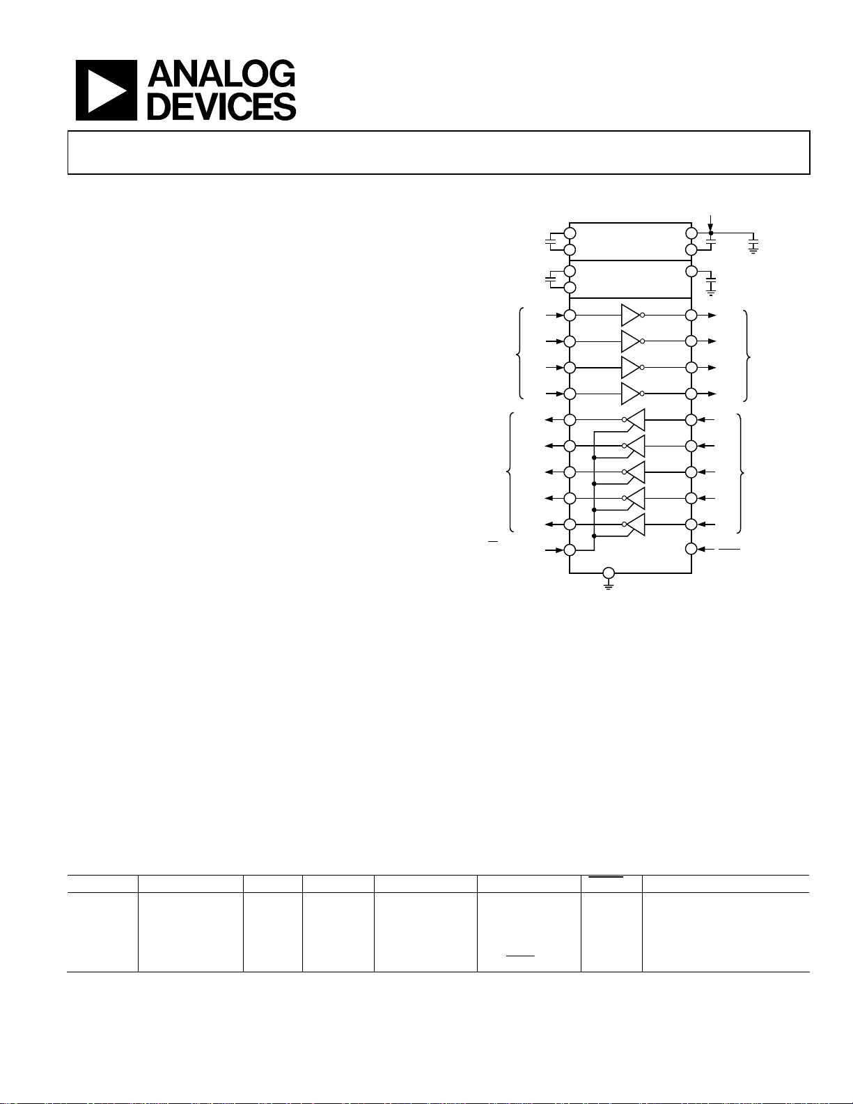
CONNECTION DIAGRAM
12
C1+
+
0.1µF
10V
+
0.1µF
10V
T1
IN
T2
IN
1
T3
IN
T4
IN
R1
OUT
R2
OUT
R3
OUT
R4
OUT
R5
OUT
)1
+5V TO +10V
C1–
C2+
C2–
VOLTAGE
DOUBLER
+10V TO –10V
VOLTAGE
INVERTER
GND
10
14
15
16
7
6
20
21
8
5
26
22
19
24
Figure 1.
Yes (EN) RW-28, RS-28, RU-28
T1
T2
T3
T4
R1
R2
R3
R4
R5
ADM211E/
ADM213E
V
CC
V+
V–
5VINPUT
11
13
17
2
3
1
28
9
4
27
23
18
25
+
+
+
0.1µF
0.1µF
6.3V
0.1µF
10V
T1
OUT
T2
OUT
RS-232
OUTPUTS
T3
OUT
T4
OUT
R1
IN
R2
IN
RS-232
R3
IN
INPUTS
R4
IN
R5
IN
SHDN (ADM211E)
SHDN (ADM213E)
2
0068-001

ADM206E/ADM207E/ADM208E/ADM211E/ADM213E
TABLE OF CONTENTS
Features.............................................................................................. 1
Applications....................................................................................... 1
General Description ......................................................................... 1
Connection Diagram ....................................................................... 1
Revision History ............................................................................... 2
Specifications..................................................................................... 3
Absolute Maximum Ratings............................................................ 4
ESD Caution.................................................................................. 4
Pin Configurations and Function Descriptions ........................... 5
Typical Performance Characteristics ............................................. 8
Theory of Operation ...................................................................... 10
Circuit Description..................................................................... 10
REVISION HISTORY
9/06—Rev. D to Rev. E
Updated Format..................................................................Universal
Changes to Figure 1 and Table 1..................................................... 1
Changes to Table 2............................................................................ 3
Changes to Figure 2, Figure 3, and Figure 5.................................. 5
Changes to Figure 7 and Figure 9................................................... 6
Changes to Figure 11........................................................................ 7
Changes to Figure 17........................................................................ 8
Updated Outline Dimensions....................................................... 16
Changes to Ordering Guide.......................................................... 19
4/05—Rev. C to Rev. D
Changes to Specifications Section.................................................. 2
Changes to Ordering Guide............................................................ 4
Updated Outline Dimensions......................................................... 6
Enable and Shutdown................................................................ 10
High Baud Rate........................................................................... 11
ESD/EFT Transient Protection Scheme .................................. 11
ESD Testing (IEC 100042) ..................................................... 11
EFT/Burst Testing (IEC 100044)........................................... 12
IEC 1000-4-3 Radiated Immunity ........................................... 13
Emissions/Interference.............................................................. 14
Conducted Emissions................................................................ 14
Radiated Emissions.................................................................... 14
Outline Dimensions....................................................................... 16
Ordering Guide .......................................................................... 19
3/01—Rev. B to Rev. C
Changes to Features Section ............................................................1
Changes to Specifications Table ......................................................2
Changes to Absolute Maximum Ratings........................................3
Changes to Figure 6 ..........................................................................5
Changes to Typical Performance Characteristics Section ...... 7, 8
Changes to Table V......................................................................... 11
Rev. E | Page 2 of 20

ADM206E/ADM207E/ADM208E/ADM211E/ADM213E
SPECIFICATIONS
VCC = 5.0 V ± 10%, C1 to C4 = 0.1 μF. All specifications T
Table 2.
Parameter Min Typ Max Unit Test Conditions/Comments
DC CHARACTERISTICS
Operating Voltage Range 4.5 5.0 5.5 V
VCC Power Supply Current 3.5 13 mA No load
SHUTDOWN SUPPLY CURRENT 0.2 10 μA
LOGIC
Input Pull-Up Current 10 25 μA TIN = GND
Input Logic Threshold Low, V
Input Logic Threshold High, V
Input Logic Threshold High, V
0.8 V
INL
2.0 V TIN
INH
2.0 V
INH
TTL/CMOS Output Voltage Low, VOL 0.4 V I
TTL/CMOS Output Voltage High, VOH 3.5 V I
TTL/CMOS Output Leakage Current +0.05 ±10 μA
RS-232 RECEIVER
Input Voltage Range
1
−30 +30 V
Input Threshold Low 0.8 1.3 V
Input Threshold High 2.0 2.4 V
Input Hysteresis 0.65 V
Input Resistance 3 5 7 kΩ TA = 0°C to 85°C
RS-232 TRANSMITTER
Output Voltage Swing ±5.0 ±9.0 V All transmitter outputs loaded with 3 kΩ to ground
Output Resistance 300 Ω VCC = 0 V, V
Output Short-Circuit Current ±6 ±20 ±60 mA
TIMING CHARACTERISTICS
Maximum Data Rate 230 kbps RL = 3 kΩ to 7 kΩ, CL = 50 pF to 2500 pF
Receiver Propagation Delay, TPHL, TPLH 0.4 2 μs CL = 150 pF
Receiver Output Enable Time, tER 120 ns
Receiver Output Disable Time, tDR 120 ns
Transmitter Propagation Delay, TPHL, TPLH 1 μs RL = 3 kΩ, CL = 2500 pF
Transition Region Slew Rate 8 V/μs
EM IMMUNITY
ESD Protection (I/O Pins) ±15 kV Human body model
±15 kV IEC 1000-4-2 air-gap discharge
±8 kV IEC 1000-4-2 contact discharge
Radiated Immunity 10 V/m IEC 1000-4-3
1
Guaranteed by design.
Table 3. ADM211E Truth Table
SHDN
0 0 Normal operation Enabled Enabled
0 1 Normal operation Enabled Disabled
1 X1 Shutdown Disabled Disabled
1
X = don’t care.
EN
Status T
1:4 R
OUT
OUT
MIN
1:5
to T
, unless otherwise noted.
MAX
T
EN,
OUT
OUT
EN = VCC, EN = GND, 0 V ≤ R
R
+3 V to −3 V or −3 V to +3 V
Table 4. ADM213E Truth Table
SHDN
0 0 Shutdown Disabled Disabled Disabled
0 1 Shutdown Disabled Disabled Enabled
1 0 Normal operation Enabled Disabled Disabled
1 1 Normal operation Enabled Enabled Enabled
EN Status T
, EN, EN, SHDN, SHDN
IN
EN, SHDN, SHDN
= 1.6 mA
= −40 μA
≤ VCC
OUT
= ±2 V
OUT
= 3 kΩ, CL = 50 pF to 2500 pF, measured from
L
1:4 R
OUT
1:3 R
OUT
OUT
4:5
Rev. E | Page 3 of 20

ADM206E/ADM207E/ADM208E/ADM211E/ADM213E
ABSOLUTE MAXIMUM RATINGS
TA = 25°C, unless otherwise noted.
Table 5.
Parameter Rating
VCC −0.3 V to +6 V
V+ (VCC – 0.3 V) to +14 V
V– +0.3 V to −14 V
Input Voltages
TIN −0.3 V to (V+ + 0.3 V)
RIN ±30 V
Output Voltages
T
±15 V
OUT
R
−0.3 V to (VCC + 0.3 V)
OUT
Short-Circuit Duration
T
Continuous
OUT
Power Dissipation
N-24-1 PDIP
(Derate 13.5 mW/°C above 70°C)
RW-24 SOIC_W
(Derate 12 mW/°C above 70°C)
RS-24 SSOP
(Derate 12 mW/°C above 70°C)
RU-24 TSSOP
(Derate 12 mW/°C above 70°C)
RW-28 SOIC_W
(Derate 12 mW/°C above 70°C)
RS-28 SSOP
(Derate 10 mW/°C above 70°C)
RU-28 TSSOP
(Derate 12 mW/°C above 70°C)
Operating Temperature Range −40°C to +85°C
Storage Temperature Range −65°C to +150°C
Lead Temperature, Soldering (10 sec) 300°C
ESD Rating
MIL-STD-883B (I/O Pins) ±15 kV
IEC 1000-4-2 Air-Gap (I/O Pins) ±15 kV
IEC 1000-4-2 Contact (I/O Pins) ±8 kV
1000 mW
900 mW
850 mW
900 mW
900 mW
900 mW
900 mW
Stresses above those listed under Absolute Maximum Ratings
may cause permanent damage to the device. This is a stress
rating only; functional operation of the device at these or any
other conditions above those indicated in the operational
section of this specification is not implied. Exposure to absolute
maximum rating conditions for extended periods may affect
device reliability.
ESD CAUTION
Rev. E | Page 4 of 20

ADM206E/ADM207E/ADM208E/ADM211E/ADM213E
T
T
T
T
PIN CONFIGURATIONS AND FUNCTION DESCRIPTIONS
TTL/CMOS
INPUTS
TL/CMOS
OUTPUTS
24
T4
OUT
23
R2
IN
22
R2
OUT
21
SHDN
20
EN
19
T4
IN
18
T3
IN
17
R3
OUT
16
R3
IN
15
V–
14
C2–
13
C2+
R1
T3
T1
T2
OUT
OUT
OUT
R1
OUT
T2
T1
GND
V
C1+
C1–
IN
IN
IN
CC
V+
1
2
3
4
5
ADM206E
6
TOP VIEW
(Not to Scale)
7
8
9
10
11
12
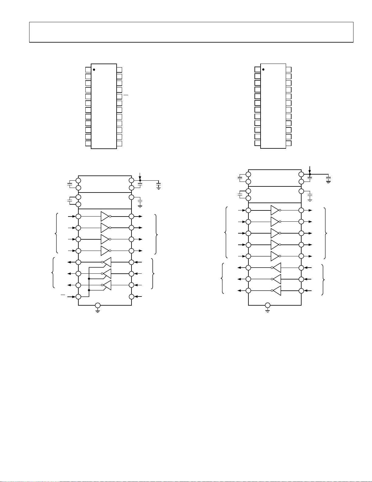
Figure 2. ADM206E Pin Configuration
1
T3
OUT
2
T1
OUT
3
T2
OUT
4
R1
IN
5
R1
OUT
ADM207E
6
T2
IN
TOP VIEW
(Not to Scale)
7
T1
IN
8
GND
9
V
CC
10
C1+
11
V+
12
00068-002
C1–
Figure 4. ADM207E Pin Configuration
24
T4
OUT
23
R2
IN
22
R2
OUT
21
T5
IN
20
T5
OUT
19
T4
IN
18
T3
IN
17
R3
OUT
16
R3
IN
15
V–
14
C2–
13
C2+
00068-004
5V INPU
5V INPU
V
10
C1+
12
13
14
7
6
18
19
5
22
17
20
C1–
C2+
C2–
+5V TO +10V
VOLTAGE
DOUBLER
+10V TO –10V
VOLTAGE
INVERTER
T1
T2
T3
T4
R1
R2
R3
ADM206E
GND
8
+
0.1µF
6.3V
+
0.1µF
16V
T1
IN
T2
IN
1
T3
IN
T4
IN
R1
OUT
R2
OUT
R3
OUT
EN
9
CC
11
V+
V–
15
2
3
1
24
4
23
16
21
0.1µF
+
6.3V
0.1µF
16V
+
T1
T2
T3
T4
R1
R2
R3
SHDN
OUT
OUT
OUT
OUT
IN
IN
IN
+
0.1µF
RS-232
OUTPUTS
RS-232
INPUTS
TTL/CMOS
INPUTS
2
TL/CMOS
OUTPUTS
0.1µF
0.1µF
1
R1
R2
R3
T1
T2
T3
T4
T5
10V
10V
OUT
OUT
OUT
10
C1+
12
13
14
7
6
18
19
21
5
22
17
C1–
C2+
C2–
+5V TO +10V
VOLTAGE
DOUBLER
+10V TO –10V
VOLTAGE
INVERTER
T1
T2
T3
T4
T5
+
+
IN
IN
IN
IN
IN
GND
8
R1
R2
R3
ADM207E
V
9
CC
+
11
V+
V–
15
+
2
3
1
24
20
4
23
16
0.1µF
6.3V
0.1µF
10V
T1
T2
T3
T4
T5
R1
R2
R3
OUT
OUT
OUT
OUT
OUT
IN
IN
IN
+
0.1µF
RS-232
OUTPUTS
RS-232
INPUTS
2
1
1
INTERNAL 400k Ω PULL-UP RESISTOR ON EACH TTL/CMOS INPUT.
2
INTERNAL 5kΩ PULL-DOWN RESISTOR ON EACH RS-232 INPUT.
Figure 3. ADM206E Typical Operating Circuit
0068-003
INTERNAL 400kΩ PULL-UP RESIST OR ON EACH TTL/CMOS INPUT.
2
INTERNAL 5kΩ PULL-DO WN RESIS TOR ON E ACH RS-232 INPUT .
Figure 5. ADM207E Typical Operating Circuit
00068-005
Rev. E | Page 5 of 20

ADM206E/ADM207E/ADM208E/ADM211E/ADM213E
T
T
TTL/CMOS
INPUTS
TTL/CMOS
OUTPUTS
1
T2
OUT
2
T1
OUT
3
R2
IN
4
R2
OUT
5
T1
IN
ADM208E
6
R1
OUT
TOP VIEW
(Not to Scale)
7
R1
IN
8
GND
9
V
CC
10
C1+
11
V+
12
C1–
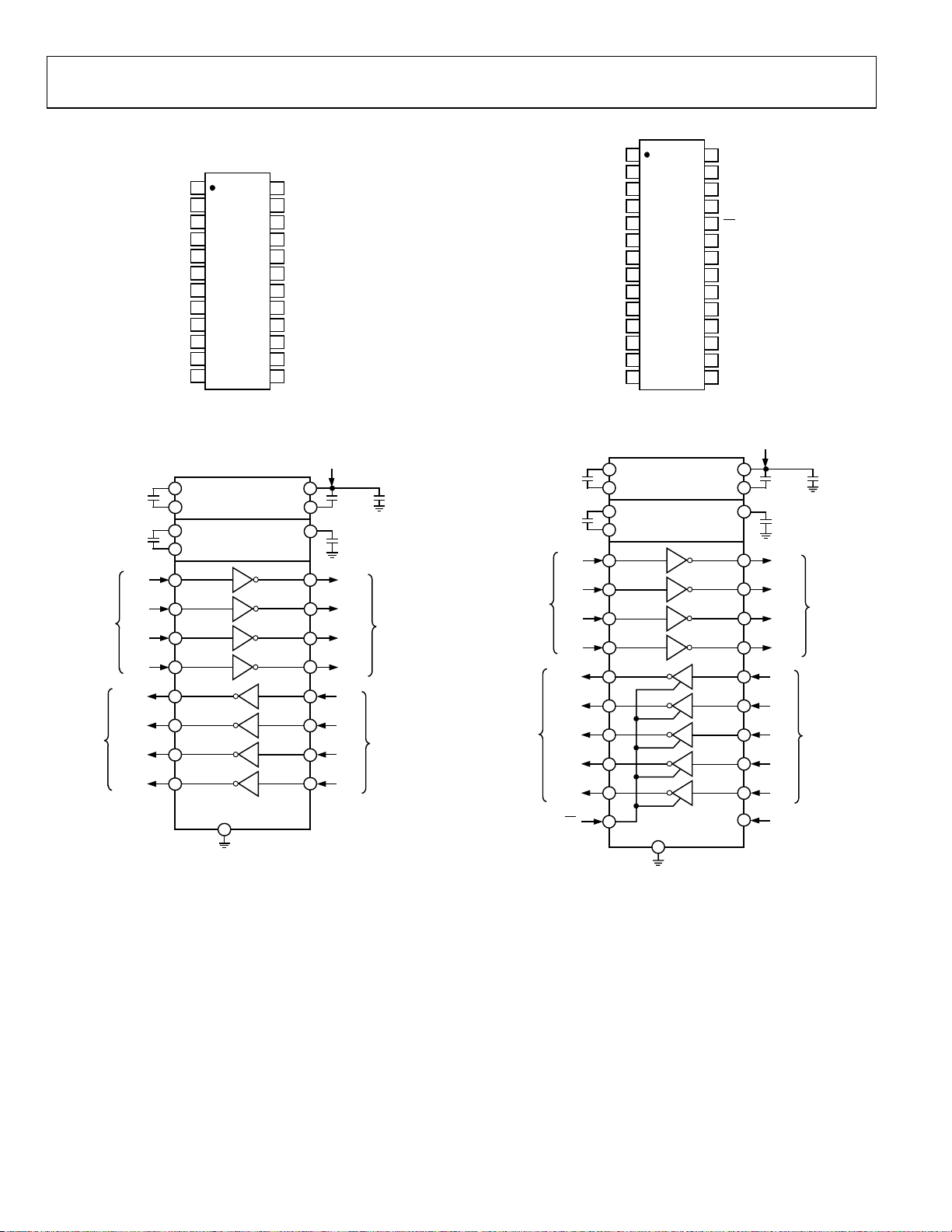
Figure 6. ADM208E Pin Configuration
10
C1+
12
13
14
5
18
19
21
6
4
22
17
C1–
C2+
C2–
+5V TO +10V
VOLTAGE
DOUBLER
+10V TO –10V
VOLTAGE
INVERTER
T1
T2
T3
T4
GND
8
+
0.1µF
10V
+
0.1µF
10V
T1
IN
T2
IN
1
T3
IN
T4
IN
R1
OUT
R2
OUT
R3
OUT
R4
OUT
24
23
22
21
20
19
18
17
16
15
14
13
V
R1
R2
R3
R4
ADM208E
T3
R3
R3
T4
T4
T3
T2
R4
R4
V–
C2–
C2+
CC
V+
V–
OUT
IN
OUT
IN
OUT
IN
IN
OUT
IN
11
15
24
20
23
16
5V INPU
9
2
1
7
3
00068-006
+
+
0.1µF
6.3V
0.1µF
10V
T1
OUT
T2
OUT
T3
OUT
T4
OUT
R1
IN
R2
IN
R3
IN
R4
IN
+
0.1µF
RS-232
OUTPUTS
RS-232
INPUTS
R2
R1
T3
T1
T2
OUT
OUT
OUT
R2
OUT
T2
T1
OUT
R1
GND
V
C1+
C1–
CC
V+
1
2
3
4
IN
5
6
IN
7
IN
8
9
IN
10
11
12
13
14
ADM211E
TOP V IEW
(Not to Scale)
28
T4
OUT
27
R3
IN
26
R3
OUT
25
SHDN
24
EN
23
R4
IN
R4
22
OUT
21
T4
IN
T3
20
IN
R5
19
OUT
R5
18
IN
17
V–
16
C2–
15
C2+
00068-008
Figure 8. ADM211E Pin Configuration
5V INPU
12
C1+
14
15
16
7
6
20
21
8
5
26
22
19
24
C1–
C2+
C2–
+5V TO +10V
VOLTAGE
DOUBLER
+10V TO –10V
VOLTAGE
INVERTER
T1
T2
T3
T4
GND
10
+
0.1µF
10V
+
0.1µF
10V
T1
IN
T2
TTL/CMOS
INPUTS
TTL/CMOS
2
OUTPUTS
IN
1
T3
IN
T4
IN
R1
OUT
R2
OUT
R3
OUT
R4
OUT
R5
OUT
EN
V
R1
R2
R3
R4
R5
ADM211E
11
CC
+
13
V+
V–
17
+
2
3
1
28
9
4
27
23
18
25
0.1µF
6.3V
0.1µF
10V
T1
OUT
T2
OUT
T3
OUT
T4
OUT
R1
IN
R2
IN
R3
IN
R4
IN
R5
IN
SHDN
+
0.1µF
RS-232
OUTPUTS
RS-232
INPUTS
2
1
INTERNAL 400k Ω PULL-UP RESISTO R ON EACH TTL /CMOS INPUT .
2
INTERNAL 5k Ω PULL-DOWN RESIST OR ON EACH RS- 232 INPUT.
Figure 7. ADM208E Typical Operating Circuit
0068-007
1
INTERNAL 400k Ω PULL-UP RESISTOR ON EACH TTL/CMOS INPUT.
2
INTERNAL 5k Ω PULL-DOW N RESISTOR O N EACH RS-232 INPUT.
Figure 9. ADM211E Typical Operating Circuit
00068-009
Rev. E | Page 6 of 20
 Loading...