Analog Devices ADM203, ADM202 Datasheet

0.1µF
6.3V
0.1µF
6.3V
0.1µF
16V
0.1µF
6.3V
+5V TO +10V
VOLTAGE
DOUBLER
+10V TO –10V
VOLTAGE
INVERTER
0.1µF
16V
+5V INPUT
V
CC
V+
V–
C1+
C1–
C2+
C2–
ADM202
6
GND
15
4
5
3
1
2
T1
IN
RS-232
OUTPUTS
TTL/CMOS
INPUTS
*
T1
OUT
T2
IN
R1
OUT
R2
OUT
T2
OUT
R1
IN
R2
IN
R1
R2
T2
T1
TTL/CMOS
OUTPUTS
RS-232
INPUTS
**
13
10
7
11
8
14
9
12
16
*
INTERNAL 400kΩ PULL-UP RESISTOR ON EACH TTL/CMOS INPUT
**INTERNAL 5kΩ PULL-DOWN RESISTOR ON EACH RS-232 INPUT
+5V INPUT
V
CC
V+
V–
C1+
C1–
C2+
C2–
GND
ADM203
7
T1
IN
RS-232
OUTPUTS
TTL/CMOS
INPUTS
*
T1
OUT
T2
IN
R1
OUT
R2
OUT
T2
OUT
R1
IN
R2
IN
R1
R2
T2
T1
TTL/CMOS
OUTPUTS
RS-232
INPUTS
**
4
1
18
2
19
5
20
3
8
13
12
17
14
11
15
10
16
V–
C2–
C2+
9
6
GND
DO NOT MAKE
CONNECTIONS TO
THESE PINS
INTERNAL
–10V POWER
SUPPLY
INTERNAL
+10V POWER
SUPPLY
High Speed, +5 V, 0.1 mF
a
FEATURES
120 kB Transmission Rate
ADM202: Small (0.1 mF) Charge Pump Capacitors
ADM203: No External Capacitors Required
Single 5 V Power Supply
Meets EIA-232-E and V.28 Specifications
Two Drivers and Two Receivers
On-Board DC-DC Converters
69 V Output Swing with +5 V Supply
Low Power BiCMOS: 2.0 mA I
630 V Receiver Input Levels
APPLICATIONS
Computers
Peripherals
Modems
Printers
Instruments
CC
CMOS RS-232 Driver/Receivers
ADM202/ADM203
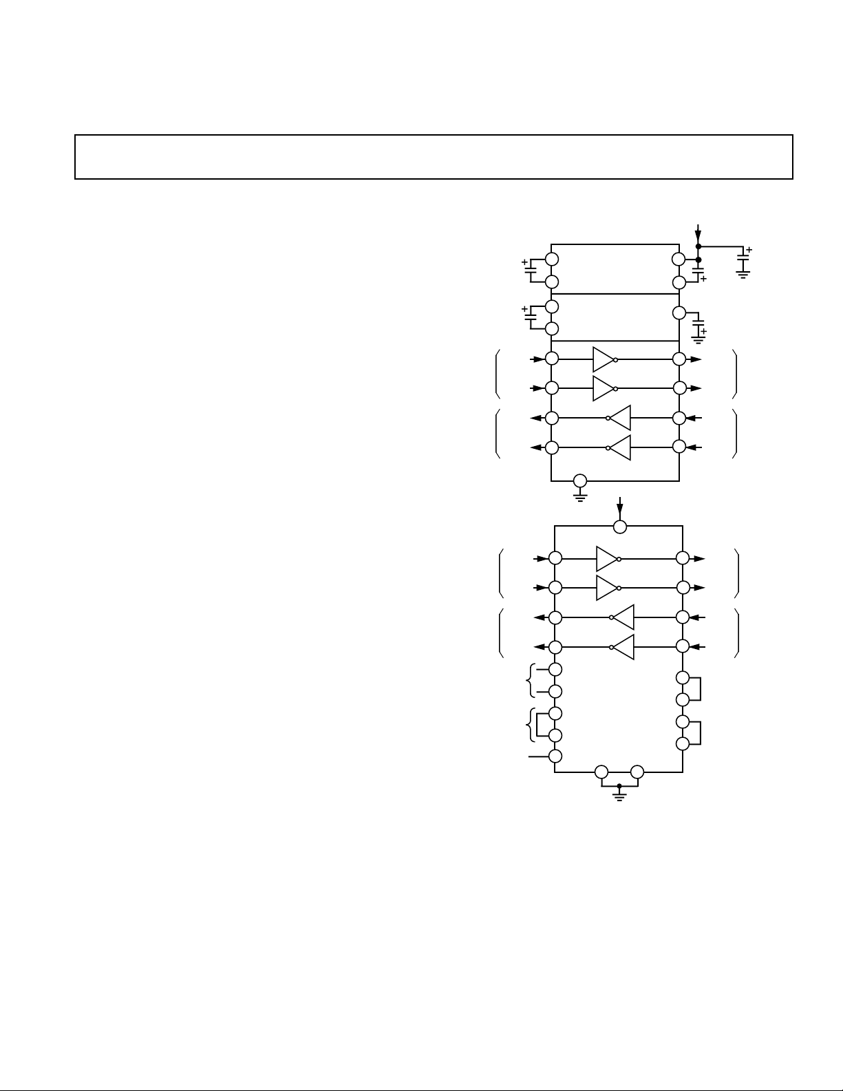
FUNCTIONAL BLOCK DIAGRAMS
GENERAL DESCRIPTION
The ADM202/ADM203 is a two-channel RS-232 line driver/
receiver pair designed to operate from a single +5 V power supply. A highly efficient on-chip charge pump design permits
RS-232 levels to be developed using charge pump capacitors as
small as 0.1 µF. The capacitors are internal to the package on
the ADM203 so no external capacitors are required. These converters generate ±10 V RS-232 output levels.
The ADM202/ADM203 meets or exceeds the EIA-232-E and
V.28 specifications. Fast driver slew rates permit operation up to
120 kB while high drive currents allows for extended cable
lengths.
An epitaxial BiCMOS construction minimizes power consumption to 10 mW and also guards against latch-up. Overvoltage
protection is provided allowing the receiver inputs to withstand
continuous voltages in excess of ± 30 V. In addition, all pins
contain ESD protection to levels greater than 2 kV.
The ADM202 is available in 16-lead DIP and both narrow and
wide SOIC packages. The ADM203 is available in a 20-pin DIP
package.
REV. 0
Information furnished by Analog Devices is believed to be accurate and
reliable. However, no responsibility is assumed by Analog Devices for its
use, nor for any infringements of patents or other rights of third parties
which may result from its use. No license is granted by implication or
otherwise under any patent or patent rights of Analog Devices.
One Technology Way, P.O. Box 9106, Norwood, MA 02062-9106, U.S.A.
Tel: 617/329-4700 Fax: 617/326-8703

(VCC = +5 V 6 10%, (ADM202 C1–C4 = 0.1 mF. All Specifications
T
to T
ADM202/ADM203–SPECIFICATIONS
MIN
Parameter Min Typ Max Units Conditions/Comments
, unless otherwise noted)
MAX
Output Voltage Swing ±5 ±9VV
= 5 V ± 5%, T1
CC
3 kΩ to GND
Output Voltage Swing ±5 ±9VV
= 5 V ± 10%, TA = +25°C, T1
CC
Loaded with 3 kΩ to GND
V
Power Supply Current. 1.5 2 mA No Load, T1IN, T2lN = V
CC
3.0 4 mA No Load, T1IN, T2IN = GND
Input Logic Threshold Low, V
Input Logic Threshold High, V
INL
INH
2.0 V T
Logic Pull-Up Current 10 25 µAT
0.8 V T
IN
IN
= 0 V
IN
RS-232 Input Voltage Range –30 +30 V
RS-232 Input Threshold Low 0.8 1.2 V
RS-232 Input Threshold High 1.7 2.4 V
RS-232 Input Hysteresis 0.2 0.5 1.0 V
RS-232 Input Resistance 3 5 7 kΩ
TTL/CMOS Output Voltage Low, V
TTL/CMOS Output Voltage High, V
Propagation Delay 0.5 5 µs RS-232 to TTL
Instantaneous Slew Rate
1
OL
3.5 V I
OH
25 30 V/µsC
Transition Region Slew Rate 5 V/µsR
0.4 V I
= 1.6 mA
OUT
= –1.0 mA
OUT
= 10 pF, R
L
= 3 kΩ, C
L
= 3–7 kΩ, TA = +25°C
L
= 2500 pF
L
Measured from +3 V to –3 V or –3 V to +3 V
Baud Rate 120 kB R
Output Resistance 300 Ω V
= 3 kΩ, C
L
= V+ = V– = 0 V, V
CC
= 1 nF
L
RS-232 Output Short Circuit Current ±10 ±60 mA
NOTE
1
Sample tested to ensure compliance.
Specifications subject to change without notice.
OUT
, T2
CC
OUT
Loaded with
OUT
OUT
= ±2 V
, T2
OUT
ABSOLUTE MAXIMUM RATINGS*
(TA = +25°C unless otherwise noted)
VCC . . . . . . . . . . . . . . . . . . . . . . . . . . . . . . . . . . . . . . . . . .+6 V
V+ . . . . . . . . . . . . . . . . . . . . . . . . . . . (VCC – 0.3 V) to +14 V
V– . . . . . . . . . . . . . . . . . . . . . . . . . . . . . . . . . . +0.3 V to –14 V
Input Voltages
T
. . . . . . . . . . . . . . . . . . . . . . . . . . –0.3 V to (VCC + 0.3 V)
IN
R
. . . . . . . . . . . . . . . . . . . . . . . . . . . . . . . . . . . . . . . .±30 V
IN
Output Voltages
T
. . . . . . . . . . . . . . . . . . . (V+, +0.3 V) to (V–, – 0.3 V)
OUT
R
. . . . . . . . . . . . . . . . . . . . . . . . –0.3 V to (VCC + 0.3 V)
OUT
Short Circuit Duration
T
. . . . . . . . . . . . . . . . . . . . . . . . . . . . . . . . . Continuous
OUT
Power Dissipation
N-16 DIP . . . . . . . . . . . . . . . . . . . . . . . . . . . . . . . . . 470 mW
R-16N SOIC . . . . . . . . . . . . . . . . . . . . . . . . . . . . . . 600 mW
R-16W SOIC . . . . . . . . . . . . . . . . . . . . . . . . . . . . . . 500 mW
N-20 DIP . . . . . . . . . . . . . . . . . . . . . . . . . . . . . . . . . 890 mW
Thermal Impedance
N-16 DIP . . . . . . . . . . . . . . . . . . . . . . . . . . . . . . . . 135°C/W
R-16N SOIC . . . . . . . . . . . . . . . . . . . . . . . . . . . . . 105°C/W
R-16W SOIC . . . . . . . . . . . . . . . . . . . . . . . . . . . . . 105°C/W
N-20 DIP . . . . . . . . . . . . . . . . . . . . . . . . . . . . . . . . 125°C/W
Operating Temperature Range
Commercial (J Version) . . . . . . . . . . . . . . . . . .0°C to +70°C
Storage Temperature Range . . . . . . . . . . . . . –65°C to +150°C
Lead Temperature Soldering
Vapor Phase (60 sec) . . . . . . . . . . . . . . . . . . . . . . . . +215°C
Infrared (15 sec) . . . . . . . . . . . . . . . . . . . . . . . . . . . . +220°C
ESD Rating . . . . . . . . . . . . . . . . . . . . . . . . . . . . . . . . .>2000 V
*This is a stress rating only and functional operation of the device at these or any
other conditions above those indicated in the operation sections of this specification is not implied. Exposure to absolute maximum rating conditions for extended
periods of time may affect reliability.
ORDERING GUIDE
Model Temperature Range Package Option
ADM202JN 0°C to +70°C N-16
ADM202JRN 0°C to +70°C R-16N
ADM202JRW 0°C to +70°C R-16W
ADM203JN 0°C to +70°C N-20
–2–
REV. 0
 Loading...