ANALOG DEVICES ADM1487 Service Manual

查询ADM1487供应商查询ADM1487供应商
PRELIMINARY TECHNICAL DATA
Ultra-Low Power RS-485/RS-422 Transceiver
a
Preliminary Technical Data
FEATURES
Low Power - 120µA Max ICC with Driver Disabled
High Input Impedance — Up to 256 Transceivers on Bus
Low-Current (1µA) Shutdown Mode
Slew Rate Control for Error-Free Data
Transmission and Low EMI
±10kV ESD Protection (Human Body Model) on
RS-485 I/O pins
Thermal Protection of Driver
Glitch-Free Driver Power-Up Allows Hot Connection
Driver Maintains High Output Impedance with Power
Off
Wide Common-Mode Range Allows ±7V Ground Differ-
ences Between Devices
Pin-Compatible with Industry Standard 75176
APPLICATIONS
Battery-Powered RS-485/RS-422 Systems
Level Translation
with Low EMI and +/-10kV ESD Protection
ADM1487
GENERAL DESCRIPTION
The ADM1487 is an ultra-low power RS-485/RS-422
transceiver consisting of one driver and one receiver per
package. Quiescent operating current is typically 80µA
and 1µA in shutdown mode. The driver and receiver both
have three-state outputs. This allows multiple drivers to be
connected to an RS-485/RS-422 bus, or several receiver
outputs to be connected to a serial data bus. The driver
will maintain a high-impedance output state even with
power off, while the receiver features fail-safe operation
that guarantees a logic high output if the inputs are left
open-circuit.
The device has slew-rate limited drivers to minimize electromagnetic interference (EMI) and reduce reflections
caused by incorrectly terminated cables.
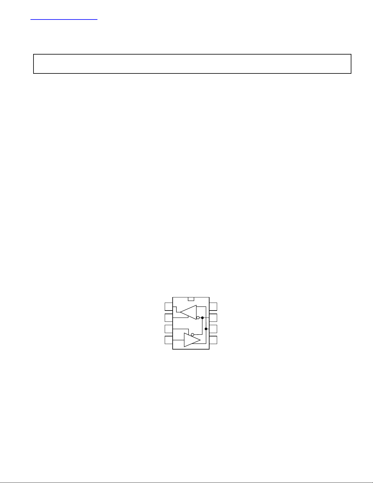
FUNCTIONAL BLOCK DIAGRAM
RO
1
2
RE
3
DE
4
DI
ADM1487
REV. PrC 08/02
Information furnished by Analog Devices is believed to be accurate and
reliable. However, no responsibility is assumed by Analog Devices for its
use, nor for any infringements of patents or other rights of third parties
which may result from its use. No license is granted by implication or
otherwise under any patent or patent rights of Analog Devices.
V
8
R
D
One Technology Way, P.O. Box 9106, Norwood, MA 02062-9106, U.S.A.
Tel: 781/329-4700 www.analog.com
Fax: 781/326-8703 Analog Devices, Inc., 2002
CC
7
B
6
A
GND
5
–1–

PRELIMINARY TECHNICAL DA T A
ADM1487
ADM1487 SPECIFICATIONS
DC ELECTRICAL CHARACTERISTICS
(VCC = +5V ±5%, TA = 0°C TO +70°C, UNLESS OTHERWISE NOTED)
Parameter Min Typ Max Units Test Conditions/Comments
Differential Driver Output Voltage,V
Differential Driver Output Voltage, V
OD1
OD2
2.0 V Figure 1, R = 50 (RS-422)
5 V Unloaded, IO = 0
1.5 5 V Figure 1, R = 27 (RS-485)
Change in Magnitude of Driver 0.2 V Figure 1, R = 27 or R = 50
Differential Output Voltage for
Complementary Output States,
VOD
Driver Common-Mode Output 3 V Figure 1, R = 27 or R = 50
Voltage, V
OC
Change in Magnitude of Driver 0.2 V R = 27 or R = 50
Common-Mode Output Voltage for
Complementary Output States, |VOC|
Input High Voltage (DE, DI, RE), V
Input Low Voltage (DE, DI, RE), V
Input Current (DE, DI, RE), I
Input Current (A, B), I
IN2
IN1
IH
IL
2V
0.8 V
±2 µA
0.30 mA DE = 0, VCC= 0V or 5.25V, VIN = 12V
-0.15 mA DE = 0, VCC = 0V or 5.25V, VIN = –7V
Differential Input Threshold Voltage -0.2 0.2 V –7V V
for Receiver, V
Receiver Input Hysteresis, V
Receiver Output High Voltage, V
Receiver Output Low Voltage, V
TH
TH
OL
OH
45 mV VCM = 0V
3.5 V IO =-4mA, VID = 200mV
0.4 V IO = 4mA, VID = –200mV
12V
CM
Three-State (High Impedance) Output ±1 µA VCC = Max, 0.4V Vo 2.4V
Current at Receive, I
Receiver Input Resistance, R
Supply Current, I
CC
OZR
IN
70 96 k –7V VCM 12V
120 200 µA No Load, Output Enabled
80 120 µA No Load, Output Disabled
Supply Current in Shutdown Mode, I
Driver Short-Circuit Ourrent, I
Driver Short-Circuit Ourrent, I
Receiver Short-Circuit Current, I
SHDN
OSD1
OSD2
OSR
1 10 µA DE = 0V, RE = V
35 250 mA V
35 250 mA V
= HIGH, –7V VO 12V
OUT
= LOW, –7V Vo 12V
OUT
7 85 mA 0V VO V
–2–
CC
OC
Rev. PrC

ADM1487 SPECIFICATIONS (continued)
ADM1487
ELECTRICAL CHARACTERISTICS
(VCC = +5V ±5%, TA = -40°C TO +85°C, UNLESS OTHERWISE NOTED)
Parameter Min Typ Max Units Test Conditions/Comments
Differential Driver Output Voltage, V
Differential Driver Output Voltage, V
OD1
OD2
2.0 V Figure 1, R = 50 (RS-422)
5 V Unloaded, IO = 0
1.5 5 V Figure 1, R = 27 (RS-485)
Driver Common-Mode 3 V Figure 1, R = 27 or R = 50
Output Voltage, V
OC
Differential Input Threshold –0.2 0.2 V –7V VCM 12V
Voltage for Receiver, V
Receiver Input Hysteresis, V
Supply Current, I
CC
TH
TH
45 mV VCM = 0V
120 200 µA No Load, Output Enabled
80 120 µA No Load, Output Disabled
Supply Current in Shutdown Mode, I
Driver Input to Output High, t
SHDN
DPLH
150 1200 ns Figures 2, 3, R
1 10 µ A DE = 0V, RE = V
DIFF
CC
= 54,
CL1 = CL2 = 100pF
Driver Input to Output Low, t
DPHL
150 1200 ns Figures 2, 3, R
DIFF
= 54,
CL1 = CL2 = 100pF
Driver Output to Output, t
SKEW
100 600 ns Figures 2, 3, R
DIFF
= 54,
CL1 = CL2 = 100pF
Driver Rise or Fall Time, t
DR
, t
DF
150 2000 ns Figures 2, 3, R
DIFF
= 54,
CL1 = CL2 = 100pF
Receiver Input to Output High, t
RPLH
30 140 250 ns Figures 2, 4, R
DIFF
= 54,
CL1 = CL2 = 100pF
Receiver Input to Output Low, t
RHL
30 140 250 ns Figures 2, 4, R
DIFF
= 54,
CL1 = CL2 = 100pF
Differential Receiver Skew, t
|t
RPLH-tRPHL
| CL1 = CL2 = 100pF
Maximum Data Rate, f
SWITCHING CHARACTERISTICS
SKD
MAX
(VCC = +5V ±5%, TA = -40°C TO +85°C, UNLESS OTHERWISE NOTED)
250 kbps
13 ns Figures 2, 4, R
DIFF
= 54,
Parameter Min Typ Max Units Test Conditions/Comments
Driver Input to Output High, t
DPLH
150 1200 ns Figures 2, 3, R
DIFF
= 54,
CL1 = CL2 = 100pF
Driver Input to Output, t
DPHL
150 1200 ns Figures 2, 3, R
DIFF
= 54,
CL1 = CL2 = 100pF
Driver Output to Output, t
SKEW
250 600 ns Figures 2, 3, R
DIFF
= 54,
CL1 = CL2 = 100pF
Driver Rise or Fall Time, t
DR
, t
DF
150 1200 ns Figures 2, 3, R
DIFF
= 54,
CL1 = CL2 = 100pF
Driver Enable to Output High, t
Driver Enable to Output Low, t
Driver Disable Time from Low, t
DZH
DZL
DLZ
100 1500 ns Figures 5, 6, CL = 100pF, S2 Closed
100 1500 ns Figures 5, 6, CL = 100pF, S1 Closed
150 1500 ns Figures 5, 6, CL = l5pF, S1 Closed
Rev. PrC –3–
 Loading...