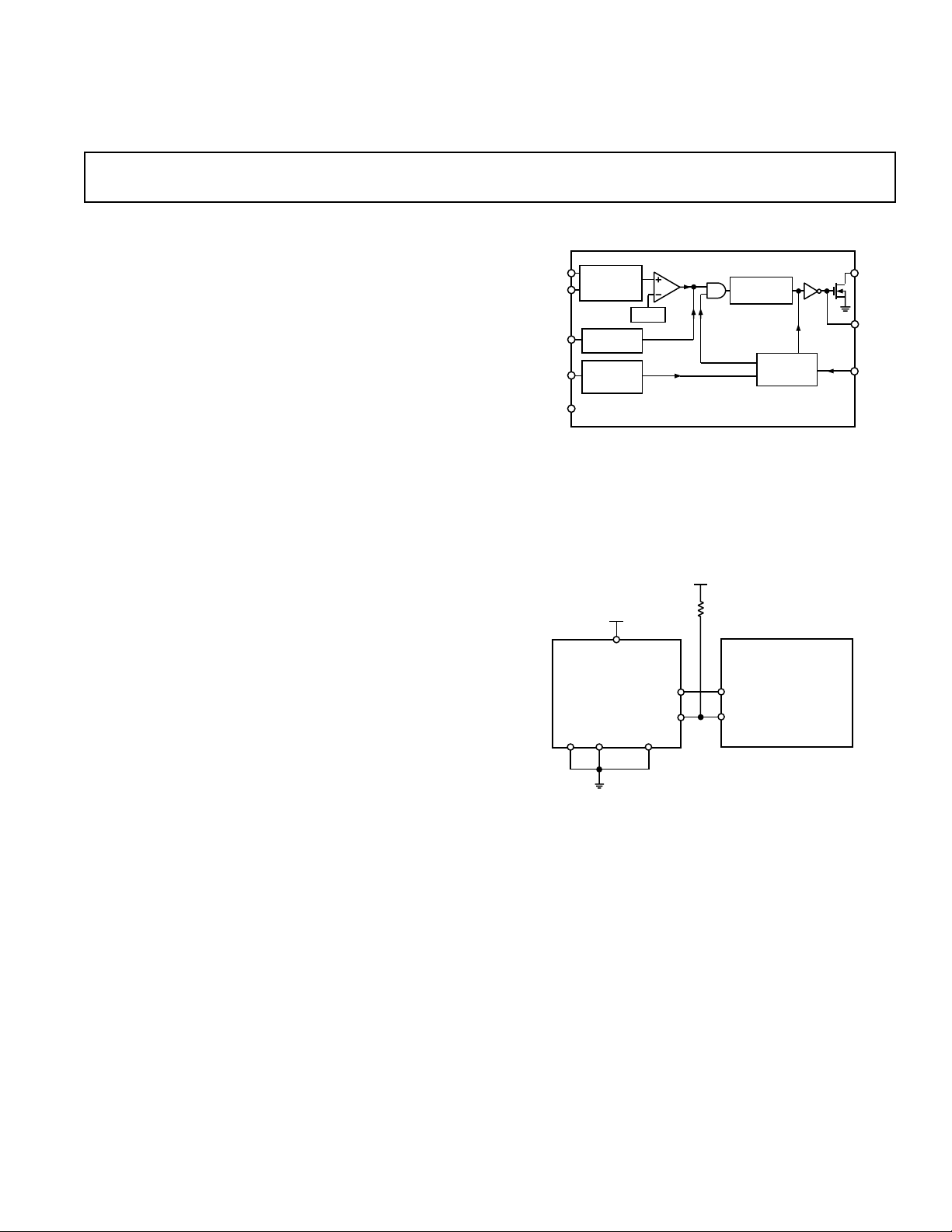
Microprocessor
GND
PB RESET
TOLERANCE
TD
RESET
STROBE
ADM1232A
RESET
GENERATOR
RESET
DEBOUNCE
WATCHDOG
TIMEBASE
SELECT
WATCHDOG
TIMER
V
CC
5%/10%
TOLERANCE
SELECT
VREF
ADM1232
ADM1232
STROBE
TOLERANCE
RESET
GND TD
ADM1232A
RESET
MICROPROCESSOR
STROBE
TOLERANCE
I/O
+5V
RESET
10kV
+5V
a
FEATURES
Superior Upgrade for MAX1232 and Dallas DS1232
Low Power Consumption (500 A max)
Adjustable Precision Voltage Monitor with +4.5 V and
+4.75 V Options
Adjustable STROBE Monitor with 150 ms, 600 ms or
1.2 sec Options
No External Components
Fast (20 ns) Strobe Pulsewidth
APPLICATIONS
Microprocessor Systems
Portable Equipment
Computers
Controllers
Intelligent Instruments
Automotive Systems
Protection Against Damage Caused by P Failure
Supervisory Circuit
ADM1232A
FUNCTIONAL BLOCK DIAGRAM
GENERAL DESCRIPTION
The ADM1232A is a superior, pin-compatible upgrade for the
MAX1232 and the DS1232LP and DS1232. The ADM1232A
can detect strobe pulsewidths as narrow as 20 ns, making it
compatible with high speed microprocessors. The Analog
Devices ADM1232A is a microprocessor monitoring circuit
that can monitor:
1. Microprocessor Supply Voltage.
2. Whether a Microprocessor has locked up.
3. An External Interrupt.
The ADM1232A is available in four different packages:
1. The ADM1232AARM in an 8-lead µSOIC (RM-8).
2. The ADM1232AAN in an 8-lead PDIP (N-8).
3. The ADM1232AARW in a 16-lead wide SOIC (R-16).
4. The ADM1232AARN is an 8-lead narrow SOIC (R-8).
Figure 1. Typical Supply Monitoring Application
REV. 0
Information furnished by Analog Devices is believed to be accurate and
reliable. However, no responsibility is assumed by Analog Devices for its
use, nor for any infringements of patents or other rights of third parties
which may result from its use. No license is granted by implication or
otherwise under any patent or patent rights of Analog Devices.
One Technology Way, P.O. Box 9106, Norwood, MA 02062-9106, U.S.A.
Tel: 781/329-4700 World Wide Web Site: http://www.analog.com
Fax: 781/326-8703 © Analog Devices, Inc., 1999

ADM1232A–SPECIFICATIONS
P
arameter Min Typ Max Units Test Conditions/Comments
(VCC = Full Operating Range, TA = T
TEMPERATURE –40 +85 °CT
MIN
= T
A
to T
unless otherwise noted)
MAX
to T
MIN
MAX
POWER SUPPLY
Voltage 4.5 5.0 5.5 V
Current 20 50 µAV
200 500 µAV
, VIH = CMOS Levels
IL
, VIH = TTL Levels
IL
STROBE AND PB RESET INPUTS
Input High Level 2.0 V
+ 0.3 V
CC
Input Low Level –0.3 +0.8 V
INPUT LEAKAGE CURRENT
(STROBE, TOLERANCE) –1.0 +1.0 µA
TD 1.6 µA
OUTPUT CURRENT
RESET 8 10 mA When V
Is at 4.5 V–5.5 V
CC
RESET, RESET –8 –12 mA When VCC Is at 4.5 V–5.5 V
OUTPUT VOLTAGE
RESET/RESET V
– 0.5 V
CC
– 0.1 V While sourcing less than 500 µA, RESET remains
CC
within 0.5 V of V
on power-down until V
CC
CC
drops below 2.0 V. While sinking less than
500 µA, RESET remains within 0.5 V of GND
on power-down until V
drops below 2.0 V.
CC
RESET/RESET High Level 0.4 V
RESET/RESET Low Level 2.4 V
1 V OPERATION
RESET Output Voltage V
– 0.1 V While Sourcing Less than 50 µA
CC
RESET Output Voltage 0.1 V While Sinking Less than 50 µA
TRIP POINT
V
CC
5% 4.5 4.62 4.74 V TOLERANCE = GND
10% 4.25 4.37 4.49 V TOLERANCE = V
CC
CAPACITANCE
Input (STROBE, TOLERANCE) 5 pF T
Output (RESET, RESET)7pFT
= +25°C
A
= +25°C
A
PB RESET
Time 20 ms PB RESET Must Be Held Low for a Minimum
Delay 1 4 20 ms of 20 ms to Guarantee a Reset
RESET ACTIVE TIME 250 610 1000 ms
STROBE
Pulsewidth 20 ns
Timeout Period 62.5 150 250 ms TD = 0 V
250 600 1000 ms TD = Floating
500 1200 2000 ms TD = V
V
CC
Fall Time 10 µ
Rise Time 0 µ
FAIL DETECT TO RESET OUTPUT DELAY
V
CC
S
S
RESET AND RESET Are Logically Correct 50 µs After V
CC
Guaranteed by Design
Guaranteed by Design
Falls Below the Set Tolerance Voltage
CC
(Figure 5)
250 610 1000 ms After VCC Rises Above the Set Tolerance Voltage
Specifications subject to change without notice.
–2–
REV. 0
 Loading...