

with Convert Pin and ALERTB Output
ADM1191
Rev. C
Trademarks and registered trademarks are the property of their respective owners.
Fax: 781.461.3113 ©2006–2012 Analog Devices, Inc. All rights reserved.
V
I
0
1
ADM1191
SENSE
SETV
VCC
CONV
MUX
I
2
C
ALERT
GND
COMPARATOR
CURRENT
SENSE
AMPLIFIER
A
SDA
SCL
A1
A0
ALERTB
05804-001
12-BIT
ADC
R
SENSE
P = VI
CONTROLLER
ADM1191
SENSEVCC
SDA
SCL
SDA
SCL
GND
ALERTB
CONV
CONV
A0
A1
3.15V TO 26V
SETV
INTERRUPT
05804-002
Data Sheet
FEATURES
Powered from 3.15 V to 26 V
Precision current sense amplifier
Precision voltage input
12-bit ADC for current and voltage readback
Convert (CONV) pin for commanding an ADC read
SETV input for setting overcurrent alert threshold
ALERTB output provides an overcurrent interrupt
2
I
C fast mode-compliant interface (400 kHz maximum)
2 address pins allow 16 devices on the same bus
10-lead MSOP
APPLICATIONS
Power monitoring/power budgeting
Central office equipment
Telecommunications and data communications equipment
PCs/servers
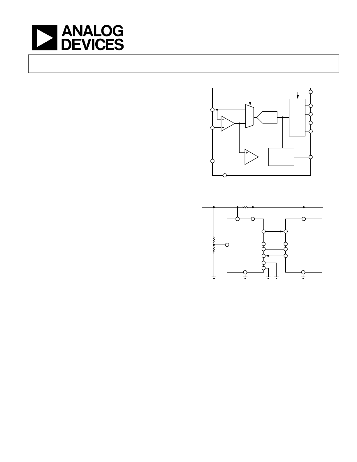
GENERAL DESCRIPTION
The ADM1191 is an integrated current sense amplifier that
offers digital current and voltage monitoring via an on-chip
12-bit analog-to-digital converter (ADC), communicated
through an I
An internal current sense amplifier measures voltage across the
sense resistor in the power path via the VCC pin and the SENSE pin.
A 12-bit ADC can measure the current seen in the sense
resistor, as well as the supply voltage on the VCC pin.
An industry-standard I
current and voltage data from the ADC. Measurements can be
initiated by an I
The CONV pin is especially useful for synchronizing reads on
multiple ADM1191 devices. Alternatively, the ADC can run
continuously, and the user can read the latest conversion data
whenever it is required. Up to 16 unique I
created, depending on the way the A0 pin and the A1 pin are
connected.
A SETV pin is also included. A voltage applied to this pin is
internally compared with the output voltage on the current
sense amplifier. The output of the SETV comparator asserts
when the current sense amplifier output exceeds the SETV
voltage. When this event occurs, the ALERTB output asserts.
Information furnished by Analog Devices is believed to be accurate and reliable. However, no
responsibility is assumed by Analog Devices for its use, nor for any infringements of patents or other
rights of third parties that may result from its use. Specifications subject to change without notice. No
license is granted by implication or otherwise under any patent or patent rights of Analog Devices.
2
C® interface.
2
C interface allows a controller to read
2
C command or via the convert (CONV) pin.
2
C addresses can be
The ALERTB output can be used as a flag to warn a microcontroller or field programmable gate array (FPGA) of an
overcurrent condition. ALERTB outputs of multiple ADM1191
devices can be tied together and used as a combined alert.
The ADM1191 is packaged in a 10-lead MSOP.
One Technology Way, P.O. Box 9106, Norwood, MA 02062-9106, U.S.A.
Tel: 781.329.4700
Digital Power Monitor
FUNCTIONAL BLOCK DIAGRAM
Figure 1.
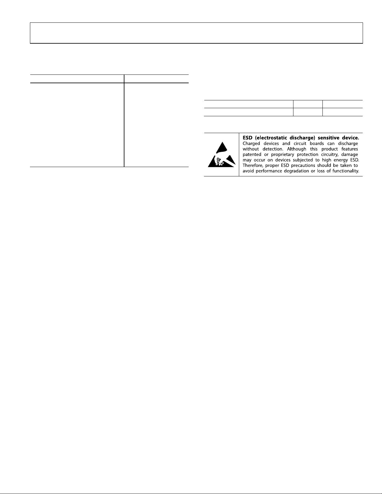
Figure 2. Applications Diagram
www.analog.com

ADM1191 Data Sheet
TABLE OF CONTENTS
Features .............................................................................................. 1
Applications ....................................................................................... 1
General Description ......................................................................... 1
Functional Block Diagram .............................................................. 1
Revision History ............................................................................... 2
Specifications ..................................................................................... 3
Absolute Maximum Ratings ............................................................ 5
Thermal Characteristics .............................................................. 5
ESD Caution .................................................................................. 5
Pin Configuration and Function Descriptions ............................. 6
Typical Performance Characteristics ............................................. 7
Voltage and Current Readback ....................................................... 9
Serial Bus Interface ....................................................................... 9
REVISION HISTORY
6/12—Rev. B to Rev. C
Added V
Changed SETV Pin Rating from 30 V to 6 V, Table 2 ................. 5
Changes to Pin 3, Pin 5, and Pin 10 Descriptions ........................ 6
Changes to Bit 2, Table 9 ................................................................ 12
Changes to ALERTB Output Section ........................................... 15
Changes to Kelvin Sense Resistor Connection Section ............. 15
Deleted Figure 27 ............................................................................ 15
Updated Outline Dimensions ....................................................... 16
2/08—Rev. A to Rev. B
Changed V
Added ADC Conversion Time Parameter .................................... 3
Changes to Input Current for 00 Decode, I
Changes to Input Current for 11 Decode, I
Added Endnote 2 .............................................................................. 4
Changes to Figure 6 .......................................................................... 7
Changes to Identifying the ADM1191 on the I
Changes to General I
Changes to Table 5 ............................................................................ 9
Changes to Figure 16 and Figure 17 ............................................. 10
Changes to Quick Command Section ......................................... 11
Changes to Figure 19 ...................................................................... 11
Changes to Table 7 .......................................................................... 11
Changes to Write Extended Command Byte Section ................ 12
Changes to Figure 21 ...................................................................... 12
Changes to Table 9 and Table 11 ................................................... 12
Changes to Converting ADC Codes to Voltage and
Current Readings Section ......................................................... 13
Changes to Figure 25 ...................................................................... 15
Change to SETV Pin Section ........................................................ 15
= 3.0 V to 5.5 V Condition to VIL and VIH, Table 1 .. 4
BUS
to VCC Throughout ................................................. 3
VCC
, Parameter ... 4
ADRL OW
, Parameter ... 4
ADRHIGH
2
2
C Timing Section, Step 3 ........................... 9
C Bus Section ......... 9
Identifying the ADM1191 on the I2C Bus ..................................9
General I2C Timing .......................................................................9
Write and Read Operations ........................................................... 11
Quick Command ........................................................................ 11
Write Command Byte ................................................................ 11
Write Extended Command Byte .............................................. 12
Read Voltage and/or Current Data Bytes ................................ 13
Applications Information .............................................................. 15
ALERTB Output ......................................................................... 15
SETV Pin ..................................................................................... 15
Kelvin Sense Resistor Connection ........................................... 15
Outline Dimensions ....................................................................... 16
Ordering Guide .......................................................................... 16
4/07—Rev. 0 to Rev. A
Changes to Table 1 ............................................................................. 3
Changes to Table 5 ............................................................................. 9
Changes to Figure 16 and Figure 17 ............................................ 10
Changes to Figure 21 ...................................................................... 12
Changes to Figure 23 and Figure 24 ............................................ 13
Added Applications Information Heading ................................. 15
9/06—Revision 0: Initial Version
Rev. C | Page 2 of 16

Data Sheet ADM1191
V
2 mA
%
−2.45
+2.45
%
V
= 50 mV
%
%
%
Low Range (VRANGE = 1)
6.65 V
High Range (VRANGE = 0)
26.52
V
µA
SPECIFICATIONS
VCC = 3.15 V to 26 V, TA = −40°C to +85°C, typical values at TA = 25°C, unless otherwise noted.
Table 1.
Parameter Min
VCC PIN
Operating Voltage Range, VCC 3.15
Supply Current, ICC 1.7
Undervoltage Lockout, V
Undervoltage Lockout Hysteresis, V
2.8
UVLO
80
UVLOHYST
CONV PIN
Input Current, I
Logic Low Threshold, V
Logic High Threshold, V
−2 +2 µA
CONV
1.2 V
CONVL
1.4 V
CONVH
MONITORING ACCURACY1
Current Sense Absolute Accuracy
0°C to +70°C −1.45
−1.8
−2.8
−5.7
0°C to +85°C −1.5
−1.8
−2.95
−6.1
−40°C to +85°C −1.95
−3.85
−6.7
V
for ADC Full Scale2 105.84
SENSE
Voltage Sense Accuracy
0°C to +70°C −0.85
−0.9 +0.9 % VCC = 10.8 V to 16.5 V (high range)
0°C to +85°C −0.85
−0.9 +0.9 % VCC = 10.8 V to 16.5 V (high range)
−40°C to +85°C −0.9
−1.15 +1.15 % VCC = 10.8 V to 16.5 V (high range)
VCC for ADC Full Scale3
Typ
Max
26
V
mV
+1.45 % V
+1.8 % V
+2.8 %
+5.7
+1.5 %
+1.8 %
+2.95 %
+6.1 %
+1.95 % V
+3.85 %
+6.7 %
mV
+0.85
+0.85
+0.9
Unit Conditions
VCC rising
= 75 mV
SENSE
= 50 mV
SENSE
V
= 25 mV
SENSE
V
= 12.5 mV
SENSE
V
= 75 mV
SENSE
V
= 50 mV
SENSE
V
= 25 mV
SENSE
V
= 12.5 mV
SENSE
= 75 mV
SENSE
SENSE
V
= 25 mV
SENSE
V
= 12.5 mV
SENSE
VCC = 3.0 V to 5.5 V (low range)
VCC = 3.0 V to 5.5 V (low range)
VCC = 3.0 V to 5.5 V (low range)
ADC Conversion Time4 150 µs
SENSE PIN
Input Current, I
SETV PIN
Overcurrent Trip Threshold 98 100 102 mV V
49.5 50 50.5 mV V
Overcurrent Trip Gain, V
Input Current, I
ALERTB PIN
Output Low Voltage, V
1 1.5 mA I
Input Current, I
−1
SENSE
/(VCC − V
SETV
−1 +1 µA V
SETVLEAK
0.05 0.1 V I
ALERTOL
ALERT
) 18 V
SENSE
−1 +1 µA V
+1
Rev. C | Page 3 of 16
V
= VCC
SENSE
= 1.8 V
SETV
= 0.9 V
SETV
= 0.9 V to 1.9 V
SETV
= 0.9 V to 1.9 V
SETV
= −100 µA
ALERT
= −2 mA
ALERT
= VCC; ALERTB not asserted
ALERT

ADM1191 Data Sheet
V
kΩ
V
Output Fall Time on SDA from V
to V
20 + 0.1 C
250
ns
C
= bus capacitance from SDA to GND
SCL Clock Frequency, f
400
kHz
Parameter Min
A0 PIN, A1 PIN
Set Address to 00, V
Set Address to 01, R
Set Address to 10, I
Set Address to 11, V
Input Current for 00 Decode, I
Input Current for 11 Decode, I
0
ADR LOWV
80
ADR LOWZ
−0.3 +0.3 µA Open state, maximum load allowed
ADRHIGHZ
2
ADRHIGHV
−40 −25
ADRLO W
ADRHIGH
I2C TIMING
Low Level Input Voltage, V
High Level Input Voltage, V
Low Level Output Voltage on SDA, V
IL
IH
OL
IHMIN
Maximum Width of Spikes Suppressed by
0.3 V
0.7 V
V V
BUS
0.4 V IOL = 3 mA
ILMAX
50 250 ns
Input Filtering on SDA and SCL Pins
Input Current, II, on SDA/SCL When Not
−10 +10 µA
Driving a Logic Low Output
Input Capacitance on SDA/SCL
SCL
Low Period of the SCL Clock
High Period of the SCL Clock
Setup Time for Repeated Start Condition, t
SDA Output Data Hold Time, t
Setup Time for a Stop Condition, t
HD ;DAT
SU;STO
Bus Free Time Between a Stop and a Start
Condition, t
BUF
Capacitive Load for Each Bus Line
1
Monitoring accuracy is a measure of the error in a code that is read back for a particular voltage/current. This is a combination of amplifier error, reference error, ADC
error, and error in ADC full-scale code conversion factor.
2
This is an absolute value to be used when converting ADC codes to current readings; any inaccuracy in this value is factored into absolute current accuracy values (see
the specifications for the Current Sense Absolute Accuracy parameter).
3
These are absolute values to be used when converting ADC codes to voltage readings; any inaccuracy in these values is factored into voltage accuracy values (see the
specifications for the Voltage Sense Accuracy parameter).
4
Time between the receipt of the command byte and the actual ADC result being placed in the register.
5 pF
600 ns
1300 ns
600 ns
SU;STA
100 900 ns
600 ns
1300 ns
400 pF
BUS
Typ
Max
0.8
120
160
5.5
3
6 µA
Unit Conditions
µA
V V
BUS
Low state
Resistor to ground state, load pin with
specified resistance for 01 decode
on the A0 pin or A1 pin for 10 decode
High state
V
= 0 V to 0.8 V
ADR
V
= 2.0 V to 5.5 V
ADR
= 3.0 V to 5.5 V
BUS
= 3.0 V to 5.5 V
BUS
BUS
Rev. C | Page 4 of 16
Data Sheet ADM1191
ABSOLUTE MAXIMUM RATINGS
Table 2.
Parameter Rating
VCC Pin 30 V
SENSE Pin 30 V
CONV Pin −0.3 V to +6 V
SETV Pin 6 V
ALERTB Pin 30 V
SDA Pin, SCL Pin −0.3 V to +6 V
A0 Pin, A1 Pin −0.3 V to +6 V
Storage Temperature Range −65°C to +125°C
Operating Temperature Range −40°C to +85°C
Lead Temperature (Soldering, 10 sec) 300°C
Junction Temperature 150°C
Stresses above those listed under Absolute Maximum Ratings
may cause permanent damage to the device. This is a stress
rating only; functional operation of the device at these or any
other conditions above those indicated in the operational
section of this specification is not implied. Exposure to absolute
maximum rating conditions for extended periods may affect
device reliability.
THERMAL CHARACTERISTICS
θJA is specified for the worst-case conditions, that is, a device
soldered in a circuit board for surface-mount packages.
Table 3. Thermal Resistance
Package Type θJA Unit
10-Lead MSOP 137.5 °C/W
ESD CAUTION
Rev. C | Page 5 of 16

ADM1191 Data Sheet
VCC
1
SENSE
2
CONV
3
GND
4
SETV
5
ALERTB
10
A1
9
A0
8
SDA
7
SCL
6
ADM1191
TOP VIEW
(Not to Scale)
05804-003
Convert Start Pin. A high level on this pin enables an ADC conversion. The state of an internal control register,
8
A0
I2C Address Pin. This pin can be tied low, tied high, left floating, or tied low through a resistor. Sixteen I2C
PIN CONFIGURATION AND FUNCTION DESCRIPTIONS
Figure 3. Pin Configuration
Table 4. Pin Function Descriptions
Pin No. Mnemonic Description
1 VCC Positive Supply Input Pin. The operating supply voltage range is from 3.15 V to 26 V. An undervoltage lockout
(UVLO) circuit resets the ADM1191 when a low supply voltage is detected.
2 SENSE Current Sense Input Pin. A sense resistor between the VCC pin and the SENSE pin generates a voltage across
a sense resistor. This voltage is proportional to the load current. A current sense amplifier amplifies this
voltage before it is digitized by the ADC.
3 CONV
which is set through the I2C interface, configures the part to convert current only, voltage only, or both
channels when the convert pin is asserted. If not required, this pin should be tied high to allow ADC to run.
4 GND Chip Ground Pin.
5 SETV Input Pin. The voltage driven onto this pin is compared with the output of the internal current sense amplifier.
The lower the voltage on the SETV, the lower the current level that causes the ALERTB output to assert.
Typical response time is 1 µs to 2 µs.
6 SCL I2C Clock Pin. Open-drain input; requires an external resistive pull-up.
7 SDA I2C Data I/O Pin. Open-drain input/output; requires an external resistive pull-up.
address options are available, depending on the external configuration of the A0 pin and the A1 pin.
9 A1 I2C Address Pin. This pin can be tied low, tied high, left floating, or tied low through a resistor. Sixteen I2C
address options are available, depending on the external configuration of the A0 pin and the A1 pin.
10 ALERTB Alert Output Pin. Active low, open-drain configuration. This pin asserts low when an overcurrent condition is
present. The level at which an overcurrent condition is detected depends on either the voltage on the SETV
pin or the value in the ALERT_TH register. The ALERT_EN register will determine which is used in the
comparison. This pin has a latching function and should be cleared manually using the ALERT_EN register.
Rev. C | Page 6 of 16

Data Sheet ADM1191
V
TYPICAL PERFORMANCE CHARACTERISTICS
2.0
1.8
1.6
1.4
1.2
1.0
(mA)
CC
I
0.8
0.6
0.4
0.2
0
0 4 8 1216202428
VCC (V)
Figure 4. Supply Current vs. Supply Voltage
05804-021
1000
900
800
700
600
500
400
300
HITS PER CO DE (1000 RE ADS)
200
100
0
2047 2048 2049 20502046
CODE
05804-060
Figure 7. ADC Noise with Current Channel, Midcode Input, and 1000 Reads
2.0
1.8
1.6
1.4
1.2
1.0
(mA)
CC
I
0.8
0.6
0.4
0.2
0
–40 806040200–20
TEMPERATURE (°C)
Figure 5. Supply Current vs. Temperature
00 DECODE 01 DECODE 10 DECODE 11 DECODE
3.2
3.0
2.8
2.6
2.4
2.2
2.0
1.8
(V)
A1
1.6
/
1.4
A0
V
1.2
1.0
0.8
0.6
0.4
0.2
0
–35 –30 –25 –20 –15 –10 –5 0 5 10
IA0/IA1 (µA)
Figure 6. Address Pin Voltage vs. Address Pin Current
for Four Addressing Options on Each Address Pin
1000
900
800
700
600
500
400
300
HITS PER CO DE (1000 RE ADS)
200
100
0
05804-022
780 781 782 783779
CODE
05804-061
Figure 8. ADC Noise with 14:1 Voltage Channel, 5 V Input, and 1000 Reads
1000
900
800
700
600
500
400
300
HITS PER CO DE (1000 RE ADS)
200
100
0
05804-026
3079 3080 3081 30823078
CODE
05804-062
Figure 9. ADC Noise with 7:1 Voltage Channel, 5 V Input, and 1000 Reads
Rev. C | Page 7 of 16

ADM1191 Data Sheet
4
3
2
1
0
–1
–2
–3
–4
0 40002500 3000 3500200015001000500
INL (LSB)
CODE
05804-023
4
3
2
1
0
–1
–2
–3
–4
0 40002500 3000 3500200015001000500
DNL (LSB)
CODE
05804-024
0
100
80
90
70
60
50
40
30
20
10
0 2.01.81.61.41.21.00.80.60.40.2
V
LIM
(mV)
V
SETV
(V)
05804-046
0
0.05
0.10
0.15
0.20
0.25
0.30
0.35
0.40
0.45
0.50
0.55
0.60
–40 806040200–20
ALERTB OUTPUT LOW (V)
TEMPERATURE (°C)
05804-047
05804-048
0
1.0
0.8
0.6
0.4
0.2
0 2 4 6 8 10 12 14 16 18 20 22 24 26 28
ALERTB OUTPUT LOW (V)
VCC (V)
0
2.0
1.6
1.2
0.8
0.4
1.8
1.4
1.0
0.6
0.2
0 3.02.82.62.42.22.01.81.61.41.21.00.80.60.40.2
ALERTB OUTPUT LOW (V)
I
LOAD
(mA)
05804-049
Figure 10. INL for ADC
Figure 11. DNL for ADC
Figure 13. ALERTB Output Low Voltage vs. Temperature @ 1 mA
Figure 14. ALERTB Output Low Voltage vs. Supply Voltage @ 1 mA
Figure 12. Overcurrent Limit Threshold vs. SETV Pin Voltage
Figure 15. ALERTB Output Low Voltage vs. Load Current
Rev. C | Page 8 of 16

Data Sheet ADM1191
Resistor to ground
Floating
01
10
0110110X
0x6C
Resistor to ground
High
01
11
0110111X
0x6E
VOLTAGE AND CURRENT READBACK
The ADM1191 contains the components to allow voltage and
current readback over an I
2
C bus. The voltage output of the
current sense amplifier and the voltage on the VCC pin are fed
into a 12-bit ADC via a multiplexer. The device can be instructed
to convert voltage and/or current at any time during operation
by issuing an I
2
C command or driving the CONV pin high. When
all conversions are complete, the voltage and/or current values
can be read back with 12-bit accuracy in two or three bytes.
SERIAL BUS INTERFACE
Control of the ADM1191 is carried out via the serial system
management bus (I
fast mode (400 kHz maximum). The ADM1191 is connected to
this bus as a slave device, under the control of a master device.
2
C). This interface is compatible with the I2C
IDENTIFYING THE ADM1191 ON THE I2C BUS
The ADM1191 has a 7-bit serial bus slave address. When the
device powers up, it does so with a default serial bus address.
The three MSBs of the address are set to 011; the four LSBs are
determined by the state of the A0 pin and the A1 pin. There are
16 configurations available on the A0 pin and A1 pin that correspond to 16 I
scheme allows 16 ADM1191 devices to operate on a single I
2
C addresses for the four LSBs (see Table 5). This
2
C bus.
GENERAL I2C TIMING
Figure 16 and Figure 17 show timing diagrams for general write
and read operations using the I
conditions for different types of read and write operations, which
are discussed in the Write and Read Operations section. The
general I
2
C protocol operates as follows:
1. The master initiates a data transfer by establishing a start
condition, defined as a high-to-low transition on the serial
data line, SDA, while the serial clock line, SCL, remains high.
This indicates that a data stream is to follow. All slave peripherals connected to the serial bus respond to the start condition
and shift in the next eight bits, consisting of a 7-bit slave
address (MSB first) plus an R/
direction of the data transfer, that is, whether data is written
to or read from the slave device (0 = write, 1 = read).
Table 5. Setting I
Base Address A1 Pin State A0 Pin State A1 Pin Logic State A0 Pin Logic State Address in Binary1 Address in Hex
011 Ground Ground 00 00 0110000X 0x60
Ground Resistor to ground 00 01 0110001X 0x62
Ground Floating 00 10 0110010X 0x64
Ground High 00 11 0110011X 0x66
Resistor to ground Ground 01 00 0110100X 0x68
Resistor to ground Resistor to ground 01 01 0110101X 0x6A
2
C Addresses via the A0 Pin and the A1 Pin
2
C. The I2C specification defines
W
bit that determines the
The peripheral whose address corresponds to the transmitted
address responds by pulling the data line low during the
low period before the ninth clock pulse, known as the
acknowledge bit, and holding it low during the high period
of this clock pulse. All other devices on the bus remain idle
while the selected device waits for data to be read from it
or written to it. If the R/
slave device. If the R/
W
bit is 0, the master writes to the
W
bit is 1, the master reads from the
slave device.
2. Data is sent over the serial bus in sequences of nine clock
pulses: eight bits of data followed by an acknowledge bit
from the slave device. Data transitions on the data line
must occur during the low period of the clock signal and
remain stable during the high period because a low-tohigh transition when the clock is high can be interpreted as
a stop signal.
If the operation is a write operation, the first data byte after
the slave address is a command byte. This tells the slave
device what to expect next. It can be an instruction, such as
telling the slave device to expect a block write, or it can be
a register address that tells the slave where subsequent data
is to be written.
Because data can flow in only one direction, as defined by
W
the R/
bit, it is not possible to send a command to a slave
device during a read operation. Before performing a read
operation, it may be necessary to first execute a write
operation to tell the slave what sort of read operation to
expect and/or the address from which data is to be read.
3. When all data bytes are read or written, stop conditions are
established. In write mode, the master pulls the data line
high during the 10
th
clock pulse to assert a stop condition.
In read mode, the master device releases the SDA line
during the SCL low period before the ninth clock pulse,
but the slave device does not pull it low. This is known as a no
acknowledge. The master then takes the data line low during
the SCL low period before the 10
during the 10
th
clock pulse to assert a stop condition.
th
clock pulse and then high
Floating Ground 10 00 0111000X 0x70
Floating Resistor to ground 10 01 0111001X 0x72
Rev. C | Page 9 of 16

ADM1191 Data Sheet
High
Floating
11
10
0111110X
0x7C
ACKNOWLEDGE BY
SLAVE
ACKNOWLEDGE BY
SLAVE
SCL
(CONTINUED)
D7 D6 D5 D4 D3 D2 D1 D0 D7 D6 D5 D4 D3 D2 D1 D0
1
9
1
9
STOP
BY
MASTER
SDA
(CONTINUED)
FRAME 3
DATA BYTE
FRAME N
DATA BYTE
SCL
START BY MASTER
1
9
1
9
D7
D6
D5
D4
D3
D2 D1
D0
ACKNOWLEDGE BY
SLAVE
ACKNOWLEDGE BY
SLAVE
FRAME 1
SLAVE ADDRESS
FRAME 2
COMMAND CODE
05804-004
SDA
A0A A0B
R/W
A1BA1A
1
1
0
SCL
START BY MASTER
1
9
1
9
D7
D6
D5
D4
D3
D2 D1
D0
ACKNOWLEDGE BY
SLAVE
ACKNOWLEDGE BY
MASTER
NO ACKNOWL E DGE
ACKNOWLEDGE BY
MASTER
FRAME 1
SLAVE ADDRESS
FRAME 2
DATA BYTE
SCL
(CONTINUED)
D7 D6 D5 D4 D3 D2 D1 D0 D7 D6 D5 D4 D3 D2 D1 D0
1
9
1
9
STOP
BY
MASTER
SDA
(CONTINUED)
FRAME 3
DATA BYTE
FRAME N
DATA BYTE
05804-005
SDA
A0A A0B
R/W
A1BA1A
1
1
0
SCLSCL
SDA
P
S
t
HD;STA
t
HD;DAT
t
HIGH
t
SU;DAT
t
SU;STA
t
HD;STA
t
F
t
R
t
LOW
t
BUF
t
SU;STO
P
S
05804-006
Base Address A1 Pin State A0 Pin State A1 Pin Logic State A0 Pin Logic State Address in Binary1 Address in Hex
Floating Floating 10 10 0111010X 0x74
Floating High 10 11 0111011X 0x76
High Ground 11 00 0111100X 0x78
High Resistor to ground 11 01 0111101X 0x7A
High High 11 11 0111111X 0x7E
1
X = don’t care.
Figure 16. General I
2
C Write Timing Diagram
Figure 17. General I
2
C Read Timing Diagram
Figure 18. Serial Bus Timing Diagram
Rev. C | Page 10 of 16

Data Sheet ADM1191
W
Write
05804-007
S
SLAVE
ADDRESS
W A
1 2 3
P
4
S
SLAVE
ADDRESS
W A
COMMAND
BYTE
A P
1 2 3 4 5 6
05804-008
divider. A 1 in C4 selects a 7:2 voltage divider. With an ADC full scale of 1.902 V, the voltage at the VCC pin for
WRITE AND READ OPERATIONS
The I2C specification defines several protocols for different
types of read and write operations. The operations used in the
ADM1191 are discussed in this section. Ta b l e 6 shows the
abbreviations used in the command diagrams (see Figure 19 to
Figure 24).
Table 6. I
2
C Abbreviations
Abbreviation Condition
S Start
P Stop
R Read
A Acknowledge
N No acknowledge
QUICK COMMAND
The quick command operation allows the master to check if the
slave is present on the bus, as follows:
1. The master device asserts a start condition on SDA.
2. The master sends the 7-bit slave address, followed by the
write bit (low).
3. The addressed slave device asserts an acknowledge on SDA.
4. The master asserts a stop condition on SDA to end the
transaction.
WRITE COMMAND BYTE
In the write command byte operation, the master device sends
a command byte to the slave device, as follows:
1. The master device asserts a start condition on SDA.
2. The master sends the 7-bit slave address, followed by the
write bit (low).
3. The addressed slave device asserts an acknowledge on SDA.
4. The master sends the command byte. The command byte
is identified by an MSB = 0. An MSB = 1 indicates an
extended register write (see the Write Extended Command
Byte section).
5. The slave asserts an acknowledge on SDA.
6. The master asserts a stop condition on SDA to end the
transaction.
Figure 20. Write Command Byte
The seven LSBs of the command byte are used to configure and
control the ADM1191. Table 7 provides details of the function
of each bit.
Figure 19. Quick Command
Table 7. Command Byte Operations
Bit Default Name Function
C0 0 V_CONT
LSB, set to convert voltage continuously. If readback is attempted before the first conversion is complete,
the ADM1191 asserts an acknowledge and returns all 0s in the returned data.
C1 0 V_ONCE Set to convert voltage once. Self-clears. I2C asserts a no acknowledge on attempted reads until the ADC
conversion is complete.
C2 0 I_CONT Set to convert current continuously. If readback is attempted before the first conversion is complete,
the ADM1191 asserts an acknowledge and returns all 0s in the returned data.
C3 0 I_ONCE Set to convert current once. Self-clears. I2C asserts a no acknowledge on attempted reads until the ADC
conversion is complete.
C4 0 VRANGE Selects different internal attenuation resistor networks for voltage readback. A 0 in C4 selects a 14:1 voltage
an ADC full-scale result is 26.52 V for VRANGE = 0 and 6.65 V for VRANGE = 1.
C5 0 N/A Unused.
C6 0 STATUS_RD Status Read. When this bit is set, the data byte read back from the ADM1191 is the status byte. It contains the
status of the device alerts. See Table 15 for full details of the status byte.
Rev. C | Page 11 of 16

ADM1191 Data Sheet
S
SLAVE
ADDRESS
W A
REGISTER
ADDRESS
A P
EXTENDED
COMMAND
BYTE
A
1 2 3 4 5 6 7 8
05804-009
1 0 EN_ADC_OC4
Enabled if four consecutive ADC conversions on the I channel exceed the threshold set in the
WRITE EXTENDED COMMAND BYTE
In the write extended command byte operation, the master
device writes to one of the three extended registers of the slave
device, as follows:
1. The master device asserts a start condition on SDA.
2. The master sends the 7-bit slave address, followed by the
write bit (low).
3. The addressed slave device asserts an acknowledge on SDA.
4. The master sends the register address byte. The MSB of
this byte is set to 1 to indicate an extended register write.
The two LSBs indicate which of the three extended registers is
to be written to (see Table 8). All other bits should be set to 0.
5. The slave asserts an acknowledge on SDA.
6. The master sends the extended command byte (refer to
Table 9, Table 10, and Table 11).
Table 9. ALERT_EN Register Operations
Bit Default Name Function
0 0 EN_ADC_OC1 LSB, enabled if a single ADC conversion on the I channel exceeds the threshold set in the ALERT_TH register.
7. The slave asserts an acknowledge on SDA.
8. The master asserts a stop condition on SDA to end the
transaction.
Figure 21. Write Extended Byte
Table 9, Table 10, and Table 11 provide the details of each
extended register.
Table 8. Extended Register Addresses
A6 A5 A4 A3 A2 A1 A0 Extended Register
0 0 0 0 0 0 1 ALERT_EN
0 0 0 0 0 1 0 ALERT_TH
0 0 0 0 0 1 1 CONTROL
ALERT_TH register.
2 0 EN_OC_ALERT Enables the OC_ALERT register. If an overcurrent condition is present compared to the SETV threshold,
the OC_ALERT register captures and latches this condition.
3 0 EN_OFF_ALERT Set this bit high to activate the SWOFF bit (see Table 11).
4 0 CLEAR Clears the OFF_ALERT, OC_ALERT, and ADC_ALERT status bits in the status register. The value of these bits
may immediately change if the source of the alert is not been cleared and the alert function is not disabled.
The CLEAR bit self-clears to 0 after the STATUS register bits have been cleared.
Table 10. ALERT_TH Register Operations
Bit Default Function
7:0 FF The ALERT_TH register sets the current level at which an alert occurs. Defaults to ADC full scale. The ALERT_TH 8-bit value
corresponds to the top eight bits of the current channel data.
Table 11. CONTROL Register Operations
Bit Default Name Function
0 0
SWOFF LSB, forces the ALERTB pin to deassert. Can be active only if the EN_OFF_ALERT bit is high (see Table 9).
Rev. C | Page 12 of 16

Data Sheet ADM1191
1
Voltage
V11
V10
V9
V8
V7
V6
V5
V4
S
SLAVE
ADDRESS
R A
DATA 1 DATA 2
N PDATA 3A
A
1 2 3 4 5 6 7 8 9 10
05804-010
S
SLAVE
ADDRESS
R A
DATA 1
N P
DATA 2
A
1 2 3 4 5
6 7 8
05804-011
05804-012
S
SLAVE
ADDRESS
STATUS
BYTE
R A
A
1 2 3 4 5
READ VOLTAGE AND/OR CURRENT DATA BYTES
Depending on how the device is configured, ADM1191 can be
set up to provide information in three ways after a conversion
(or conversions): voltage and current readback, voltage only
readback, and current only readback. See the Write Command
Byte section for more details.
Voltage and Current Readback
The ADM1191 digitizes both voltage and current. Three bytes
are read back in the format shown in Tabl e 12.
Table 12. Voltage and Current Readback
Byte Contents B7 B6 B5 B4 B3 B2 B1 B0
1 Voltage
V11 V10 V9 V8 V7 V6 V5 V4
MSBs
2 Current
I11 I10 I9 I8 I7 I6 I5 I4
MSBs
3 LSBs V3 V2 V1 V0 I3 I2 I1 I0
Voltage Readback
The ADM1191 digitizes voltage only. Two bytes are read back in
the format shown in Tab l e 13.
Table 13. Voltage Only Readback Format
Byte Contents B7 B6 B5 B4 B3 B2 B1 B0
MSBs
2 Voltage
V3 V2 V1 V0 0 0 0 0
LSBs
Current Readback
The ADM1191 digitizes current only. Two bytes are read back
in the format shown in Table 14.
Table 14. Current Only Readback Format
Byte Contents B7 B6 B5 B4 B3 B2 B1 B0
1 Current
I11 I10 I9 I8 I7 I6 I5 I4
MSBs
2 Current
I3 I2 I1 I0 0 0 0 0
LSBs
The following series of events occurs when the master receives
three bytes (voltage and current data) from the slave device:
1. The master device asserts a start condition on SDA.
2. The master sends the 7-bit slave address, followed by the
read bit (high).
3. The addressed slave device asserts an acknowledge on SDA.
4. The master receives the first data byte.
5. The master asserts an acknowledge on SDA.
6. The master receives the second data byte.
7. The master asserts an acknowledge on SDA.
8. The master receives the third data byte.
9. The master asserts a no acknowledge on SDA.
10. The master asserts a stop condition on SDA, and the
transaction ends.
For cases where the master is reading voltage only or current
only, two data bytes are read and Step 7 and Step 8 are not required.
Figure 22. Three-Byte Read from ADM1191
Figure 23. Two-Byte Read from ADM1191
Converting ADC Codes to Voltage and Current Readings
Equation 1 and Equation 2 can be used to convert ADC codes
representing voltage and current from the ADM1191 12-bit ADC
into actual voltage and current values.
Voltage = (V
/4096) × Code (1)
FULLSCALE
where:
V
= 6.65 V (7:2 range) or 26.52 V (14:1 range).
FULLSCALE
Code is the ADC voltage code read from the device
(Bit V11 to Bit V0).
Current = ((I
/4096) × Code)/Sense Resistor (2)
FULLSCALE
where:
I
FULLSCALE
= 105.84 mV.
Code is the ADC current code read from the device
(Bit I11 to Bit I0).
Read Status Register
A single register of status data can also be read from the
ADM1191 as follows:
1. The master device asserts a start condition on SDA.
2. The master sends the 7-bit slave address, followed by the
read bit (high).
3. The addressed slave device asserts an acknowledge on SDA.
4. The master receives the status byte.
5. The master asserts an acknowledge on SDA.
Figure 24. Status Read from ADM1191
Table 15 shows the ADM1191 STATUS registers in detail. Note
that Bit 1, Bit 3, and Bit 5 are cleared by writing to Bit 4 (the
CLEAR bit) of the ALERT_EN register.
Rev. C | Page 13 of 16

ADM1191 Data Sheet
Table 15. Status Byte Operations
Bit Name Function
0 ADC_OC An ADC-based overcurrent comparison is detected on the last three conversions.
1 ADC_ALERT An ADC-based overcurrent trip has occurred, causing the alert. Cleared by writing to Bit 4 of the ALERT_EN register.
2 OC An overcurrent condition is present (that is, the output of the current sense amplifier is greater than the voltage on the
SETV input).
3 OC_ALERT An overcurrent condition causes the ALERT block to latch a fault, and the ALERTB output asserts. Cleared by writing to
Bit 4 of the ALERT_EN register.
4 OFF_STATUS Set to 1 by writing to the SWOFF bit of the CONTROL register.
5 OFF_ALERT An alert has been caused by the SWOFF bit. Cleared by writing to Bit 4 of the ALERT_EN register.
Rev. C | Page 14 of 16

Data Sheet ADM1191
R
SENSE
P = VI
CONTROLLER
ADM1191
SENSEVCC
SDA
SCL
SDA
SCL
GND
ALERTB
CONV
CONV
A0
A1
3.15V TO 26V
SETV
INTERRUPT
05804-013
ADM1191
SETV
ALERT
CURRENT
SENSE
AMPLIFIER
A
ALERTB
R
SENSE
I
LOAD
APPLIED
VOLTAGE
SENSEVCC
COMPARATOR
05804-014
APPLICATIONS INFORMATION
ALERTB OUTPUT
The ALERTB output is an open-drain pin with 30 V tolerance.
This output can be used as an overcurrent flag by connecting it
to the general-purpose logic input of a controller. During normal
operation, this output is pulled high (an external pull-up resistor
should be used because this is an open-drain pin). When an
overcurrent condition occurs, the ADM1191 pulls this output low.
The ALERTB pin is disabled by default on power up. See the
ALERT_EN register to enable.
condition at a different current level, with a gain of 18. See
Figure 12 for an illustration of this relationship.
Figure 25. Using the ALERTB Output as an Interrupt
SETV PIN
The SETV pin allows the user to adjust the current level that
trips the ALERTB output. The output of the current sense amplifier
is compared with the voltage driven onto the SETV pin. If the
current sense amplifier output is higher than the SETV voltage,
the output of the comparator asserts. By driving a different
voltage onto the SETV pin, the ADM1191 detects an overcurrent
Figure 26. SETV Operation
KELVIN SENSE RESISTOR CONNECTION
When using a low value sense resistor for high current
measurement, the problem of parasitic series resistance can
arise. The pad and solder resistance can be a substantial fraction
of the rated resistance, making the total resistance larger than
expected. This error problem can be largely avoided by using a
Kelvin sense connection. This type of connection separates the
high current path through the resistor and the voltage drop
across the resistor. A 4-pad resistor may be used or a split pad
layout can be used with a 2-pad sense resistor to achieve Kelvin
sensing.
Rev. C | Page 15 of 16

ADM1191 Data Sheet
COMPLIANT TO JEDEC STANDARDS MO-187-BA
091709-A
6°
0°
0.70
0.55
0.40
5
10
1
6
0.50 BSC
0.30
0.15
1.10 MAX
3.10
3.00
2.90
COPLANARITY
0.10
0.23
0.13
3.10
3.00
2.90
5.15
4.90
4.65
PIN 1
IDENTIFIER
15° MAX
0.95
0.85
0.75
0.15
0.05
©2006–2012 Analog Devices, Inc. All rights reserved. Trademarks and
OUTLINE DIMENSIONS
ORDERING GUIDE
Model1 Temperature Range Package Description Package Option Branding
ADM1191-2ARMZ-R7 −40°C to +85°C 10-Lead MSOP RM-10 M5L
EVAL-ADM1191EBZ Evaluation Board
1
Z = RoHS Compliant Part.
Purchase of licensed I2C components of Analog Devices, Inc., or one of its sublicensed Associated Companies conveys a license for the purchaser under the Philips I2C
Patent Rights to use these components in an I
registered trademarks are the property of their respective owners.
D05804-0-6/12(C)
2
C system, provided that the system conforms to the I2C Standard Specification as defined by Philips.
Figure 27. 10-Lead Mini Small Outline Package [MSOP]
(RM-10)
Dimensions shown in millimeters
Rev. C | Page 16 of 16
 Loading...