

V
www.BDTIC.com/ADI
Quad Voltage Monitor and Sequencer
FEATURES
Powered from 2.7 V to 5.5 V on the VCC pin
Monitors 4 supplies via 0.8% accurate comparators
Logical core with internal timeouts provides power supply
sequencing an
4 inputs can be programmed to monitor different voltage
vels with resistor dividers
le
3 open-drain enable outputs
Open-drain power-good output (PWRGD)
10-lead MSOP
APPLICATIONS
Monitor and alarm functions
Power supply sequencing
Telecommunication and data communication equipment
PCs/servers
GENERAL DESCRIPTION
The ADM1185 is an integrated, 4-channel, voltage monitoring
and sequencing device. A 2.7 V to 5.5 V power supply is
required on the VCC pin to power the device.
Four precision comparators monitor four voltage rails.
Al
l comparators have a 0.6 V reference with a worst-case
accuracy of 0.8%. Resistor networks that are external to the
VIN1, VIN2, VIN3, and VIN4 pins set the trip points for
the monitored supply rails.
A digital core interprets the status of the comparator outputs.
d fault protection
ADM1185
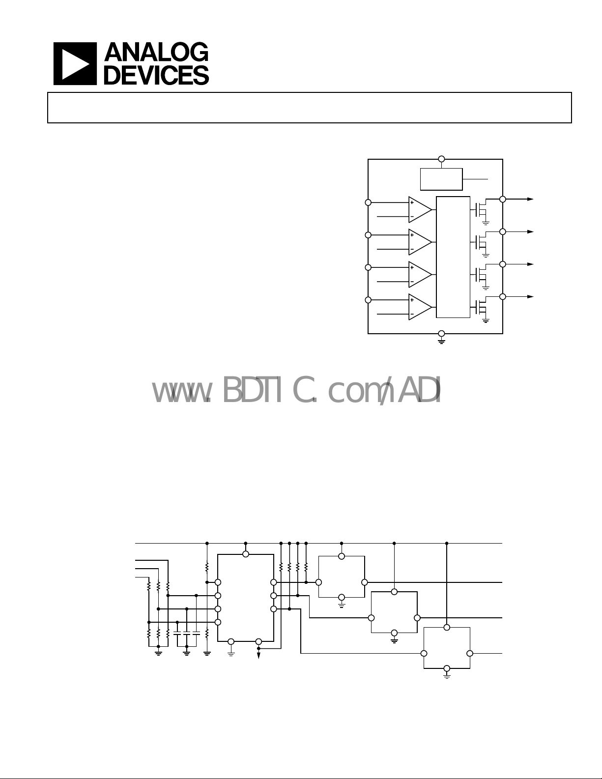
FUNCTIONAL BLOCK DIAGRAM
CC
POWER AND
ADM1185
VIN1
REF = 0.6V
VIN2
REF = 0.6V
VIN3
REF = 0.6V
VIN4
REF = 0.6V
REFERENCE
GENERATOR
GND
Figure 1.
Internal time delays can be used for sequencing the startup of
s
ubsequent power supplies enabled by the outputs. Supplies
falling out of range are also detected and, as a result, appropriate
outputs are disabled.
The ADM1185 has four open-drain outputs. In a typical
co
nfiguration, OUT1 to OUT3 are used to enable power
supplies, while PWRGD is a common power-good output,
indicating the status of all monitored supplies.
The ADM1185 is available in a 10-lead mini small outline
pa
ckage (MSOP).
STATE
MACHINE
CORE
REF = 0.6V
OUT1
OUT2
OUT3
PWRGD
06196-001
APPLICATIONS DIAGRAM
3.3V IN
2.5V OUT
1.8V OUT
1.2V OUT
Rev. A
Information furnished by Analog Devices is believed to be accurate and reliable. However, no
responsibility is assumed by Anal og Devices for its use, nor for any infringements of patents or ot her
rights of third parties that may result from its use. Specifications subject to change without notice. No
license is granted by implication or otherwise under any patent or patent rights of Analog Devices.
Trademarks and registered trademarks are the property of their respective owners.
VCC
ADM1185
OUT1VIN1
OUT2VIN2
OUT3VIN3
VIN4
GND PWRGD
POWER
GOOD
IN
REGULATOR1
EN OUT
GND
Figure 2.
One Technology Way, P.O. Box 9106, Norwood, MA 02062-9106, U.S.A.
Tel: 781.329.4700 www.analog.com
Fax: 781.461.3113 ©2007 Analog Devices, Inc. All rights reserved.
IN
REGULATOR2
EN OUT
GND
IN
REGULATOR3
EN OUT
GND
2.5V OUT
1.8V OUT
1.2V OUT
06196-002

ADM1185
www.BDTIC.com/ADI
TABLE OF CONTENTS
Features.............................................................................................. 1
Applications....................................................................................... 1
Functional Block Diagram .............................................................. 1
General Description ......................................................................... 1
Applications Diagram ......................................................................1
Revision History ............................................................................... 2
Specifications..................................................................................... 3
Absolute Maximum Ratings............................................................ 4
Thermal Resistance ...................................................................... 4
REVISION HISTORY
11/07—Rev. 0 to Rev. A
Changes to Table 5............................................................................ 9
Changes to Figure 20 and Figure 21............................................. 11
3/07—Revision 0: Initial Version
ESD Caution...................................................................................4
Pin Configuration and Function Descriptions..............................5
Typical Performance Characteristics..............................................6
Theory of Operation .........................................................................9
Power-On Sequencing and Monitoring.....................................9
Voltage Monitoring After Power-On....................................... 10
Cascading Multiple Devices...................................................... 12
Outline Dimensions....................................................................... 13
Ordering Guide .......................................................................... 13
Rev. A | Page 2 of 16

ADM1185
www.BDTIC.com/ADI
SPECIFICATIONS
V
= 2.7 V to 5.5 V, TA = −40°C to +85°C, unless otherwise noted.
CC
Table 1.
Parameter Min Typ Max Unit Conditions
VCC PIN
Operating Voltage Range, VCC 2.7 3.3 5.5 V
Supply Current, I
VIN1 TO VIN4 (VINx) PINS
Input Current, I
Input Rising Threshold, V
OUT1 TO OUT3 (OUTx), PWRGD PINS
Output Low Voltage, V
0.4 V VCC = 1 V, I
Leakage Current, I
VCC that Guarantees Valid Outputs 1 V
TIMING DELAYS
VIN1 to OUT1 Rising Delay 100 190 280 ms VCC = 3.3 V, see Figure 7
VIN4 to PWRGD Rising Delay 100 190 280 ms VCC = 3.3 V, see Figure 7
VIN2 to OUT2, VIN3 to OUT3
Low-to-High Propagation Delay 30 μs VCC = 3.3 V, see Figure 9
High-to-Low Propagation Delay, All Inputs 30 μs VCC = 3.3 V, see Figure 10
24 80 μA
VCC
−20 +20 nA V
VINLEAK
THR
0.4 V VCC = 2.7 V, I
OUTL
ALERT
0.5952 0.6000 0.604
8
−1 +1 μA
= 0.7 V
VINx
V
= 2 mA
SINK
= 100 μA
SINK
All outputs are guaranteed to be either low or giving
alid output level from V
a v
Delays only applicable to certain operations states;
fer to state diagram (Figure 19) for more details
re
= 1 V
CC
Rev. A | Page 3 of 16
ADM1185
www.BDTIC.com/ADI
ABSOLUTE MAXIMUM RATINGS
TA = 25°C, unless otherwise noted.
Table 2.
Parameter Rating
VCC Pin −0.3 V to +6 V
VINx Pins −0.3 V to +6 V
OUTx, PWRGD Pins −0.3 V to +6 V
Storage Temperature Range −65°C to +125°C
Operating Temperature Range −40°C to +85°C
Lead Temperature Soldering (10 sec) 300°C
Junction Temperature 150°C
Stresses above those listed under Absolute Maximum Ratings
may cause permanent damage to the device. This is a stress
rating only; functional operation of the device at these or any
other conditions above those indicated in the operational
section of this specification is not implied. Exposure to absolute
maximum rating conditions for extended periods may affect
device reliability.
THERMAL RESISTANCE
θJA is specified for the worst-case conditions, that is, a device
soldered in a circuit board for surface-mount packages.
Table 3. Thermal Resistance
Package Type θJA Unit
10-Lead MSOP 137.5 °C/W
ESD CAUTION
Rev. A | Page 4 of 16

ADM1185
V
V
V
V
www.BDTIC.com/ADI
PIN CONFIGURATION AND FUNCTION DESCRIPTIONS
GND
1
IN1
2
ADM1185
3
IN2
TOP VIEW
(Not to Scale)
4
IN3
IN4
5
Figure 3.
Table 4. Pin Function Descriptions
Pin No. Mnemonic Description
1 GND Chip Ground Pin.
2 VIN1
Noninverting Input of Comparator 1. The voltage on this pin is
monitor a voltage rail via a resistor divider. The output of this comparator is monitored by the state machine core.
This input can also be driven by a logic signal to initiate a power-up sequence.
3 VIN2
Noninverting Input of Comparator 2. The voltage on this pin is
monitor a voltage rail via a resistor divider. The output of this comparator is monitored by the state machine core.
4 VIN3
Noninverting Input of Comparator 3. The voltage on this pin is
monitor a voltage rail via a resistor divider. The output of this comparator is monitored by the state machine core.
5 VIN4
Noninverting Input of Comparator 4. The voltage on this pin is
monitor a voltage rail via a resistor divider. The output of this comparator is monitored by the state machine core.
6 PWRGD
Active-High, Open-Drain Output. This output is pulled low
exceeds 0.6 V, the state machine moves from STATE4 to STATE5, and PWRGD is asserted. Once in STATE5 (the
PWRGD state), this output is driven low if the voltage on VIN1, VIN2, VIN3, or VIN4 falls below 0.6 V.
7 OUT3
Active-High, Open-Drain Output. This output is pulled low onc
the state machine moves from STATE3 to STATE4, and OUT3 is asserted. Once the power-up sequence is complete
and STATE5 (the PWRGD state) is reached, this output is driven low if the voltage on VIN1 falls below 0.6 V.
8 OUT2
Active-High, Open-Drain Output. This output is pulled low onc
the state machine moves from STATE2 to STATE3, and OUT2 is asserted. Once the power-up sequence is complete
and STATE5 (the PWRGD state) is reached, this output is driven low if the voltage on VIN1 falls below 0.6 V.
9 OUT1
Active-High, Open-Drain Output. This output is pulled low onc
the state machine moves from STATE1 to STATE2, and OUT1 is asserted. A time delay of 190 ms (typical) is included
before the assertion of this pin. Once the power-up sequence is complete and STATE5 (the PWRGD state) is
reached, this output is driven low if the voltage on VIN1 falls below 0.6 V.
10 VCC Positive Supply Input Pin. The operating supply voltage range is 2.7 V to 5.5 V.
10
9
8
7
6
VCC
OUT1
OUT2
OUT3
PWRGD
06196-003
compared with a 0.6 V reference. Can be used to
compared with a 0.6 V reference. Can be used to
compared with a 0.6 V reference. Can be used to
compared with a 0.6 V reference. Can be used to
once VCC = 1 V. When the voltage on each VINx input
e VCC = 1 V. When the voltage on VIN3 exceeds 0.6 V,
e VCC = 1 V. When the voltage on VIN2 exceeds 0.6 V,
e VCC = 1 V. When the voltage on VIN1 exceeds 0.6 V,
Rev. A | Page 5 of 16
ADM1185
www.BDTIC.com/ADI
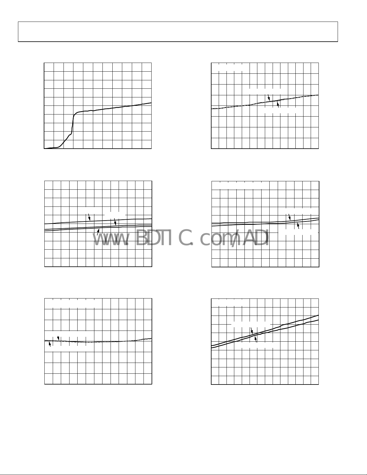
TYPICAL PERFORMANCE CHARACTERISTICS
50
45
40
35
30
25
20
15
SUPPLY CURRENT (µA)
10
5
0
05
SUPPLY VOLTAGE (V)
.5
5.04.54.03.53.02.52.01.51.00.5
06196-004
Figure 4. Supply Current vs. Supply Voltage
280
100mV OVERDRIVE
260
240
220
200
180
RISING DEL AY (ms)
160
140
120
2.7 5.55.35.14.94. 74.54.34.13.93.5 3.73.33.12.9
VIN4 TO PWRG D DELAY
VIN1 TO OUT1 DELAY
SUPPLY VOLTAGE (V)
Figure 7. VIN1/VIN4 to OUT1/PWRGD Rising Delay vs. Supply Voltage
06196-012
50
45
40
35
30
25
20
15
SUPPLY CURRENT (µA)
10
5
0
–40 9070 806050403020100–10–20–30
VCC = 5V
TEMPERATURE (°C)
VCC = 3.3V
VCC = 2.7V
Figure 5. Supply Current vs. Temperature
280
VCC = 3.3V, 100mV OVERDRIV E
260
240
220
VIN4 TO PW RGD DELAY
200
VIN1 TO OUT1 DELAY
180
RISING DEL AY (ms)
160
140
120
–40 –30 –20 –10 0 908070605040302010
TEMPERATURE (°C)
Figure 6. VIN1/VIN4 to OUT1/PWRGD Rising Delay vs. Temperature
50
VCC = 3.3V, 100mV OVERDRIVE
45
40
35
30
25
20
RISING DEL AY (µs)
15
10
5
0
–40 9080706050403020010–10–20–30
06196-005
TEMPERATURE (°C)
VIN3 TO O UT3 DELAY
VIN2 TO OUT2 DELAY
06196-013
Figure 8. VIN2/VIN3 to OUT2/OUT3 Rising Delay vs. Temperature
50
100mV OVERDRIVE
45
40
35
30
25
20
RISING DELAY (µs)
15
10
5
0
2.7 5.55.1 5.34.94.74.54.34. 13.93.5 3.73. 33.12.9
06196-011
VIN3 TO OUT3 DELAY
VIN2 TO OUT2 DELAY
SUPPLY VOLTAGE (V)
06196-014
Figure 9. VIN2/VIN3 to OUT2/OUT3 Rising Delay vs. Supply Voltage
Rev. A | Page 6 of 16

ADM1185
www.BDTIC.com/ADI
60
100mV OVERDRIVE
50
40
30
20
FALLING DELAY (µs)
10
0
2.7 5.55.1 5.34.94.74.54.34. 13.93.5 3.73. 33.12.9
VOLTAGE (V)
Figure 10. VIN1 to OUT1 Falling Delay vs. Supply Voltage
06196-016
180
160
140
120
100
80
60
40
MAXIMUM TRANSI ENT DURATIO N (µs)
20
0
019070 80605040302010
INPUT OVERDRI VE (mV)
00
06196-007
Figure 13. Trip Threshold Maximum Transient Duration vs. Input Overdrive
50
VCC = 3.3V, 100mV OVERDRIV E
40
30
20
FALLING DELAY (µs)
10
0
–40 –30 –20 –10 0 10 20 30 40 50 60 70 80 90
Figure 11. VINx to Output Fall
0.610
0.608
0.606
0.604
0.602
0.600
0.598
0.596
VINx TRIP THRESHOLD (V)
0.594
0.592
0.590
–40 9070 806050403020100–10–20–30
TEMPERATURE (°C)
ing Delay vs. Temperature
TEMPERATURE (°C)
Figure 12. VINx Trip Threshold vs. Temperature
200
180
160
140
120
100
80
60
PROPAGATI ON DELAY (µ s)
40
20
0
0 102030405060708090100
06196-015
INPUT OVERDRI VE (mV)
APPLICABLE ONLY TO
CHANNEL 2 AND CHANNEL 3
06196-017
Figure 14. Propagation Delay vs. Input Overdrive
400
350
300
250
200
150
100
OUTPUT LOW VOLTAGE (mV)
50
0
02222018161412108642
06196-006
OUTPUT SINK CURRENT (mA)
4
06196-018
Figure 15. Output Low Voltage vs. Output Sink Current
Rev. A | Page 7 of 16

ADM1185
www.BDTIC.com/ADI
100
90
80
70
60
50
40
1mA SINK
30
OUTPUT LOW VOLTAGE (mV)
20
10
100µA SINK
0
1.0 5.55.04.54.03.53.02.52.01.5
Figure 16. Output Low Voltage vs. Supply Voltage
SUPPLY VOLTAGE (V)
06196-019
Rev. A | Page 8 of 16

ADM1185
V
www.BDTIC.com/ADI
THEORY OF OPERATION
The operation of the ADM1185 is explained in this section in
the context of the device in a voltage monitoring and sequencing
application (see
itors four separate voltage rails, turns on three regulators in
mon
Figure 18). In this application, the ADM1185
a predefined sequence, and generates a power-good signal to
turn on a controller when all power supplies are up and stable.
POWER-ON SEQUENCING AND MONITORING
The main supply, in this case 3.3 V, powers up the device via the
VCC pin as the voltage rises. A supply voltage of 2.7 V to 5.5 V
is needed to power the device.
The VIN1 pin monitors the main 3.3 V supply. An external
esistor divider scales this voltage down for monitoring at the
r
VIN1 pin. The resistor ratio is chosen so that the VIN1 voltage
is 0.6 V when the main voltage rises to the preferred level at startup (a voltage below the nominal 3.3 V level). R1 is 4.6 kΩ and
R2 is 1.2 kΩ, so a voltage level of 2.9 V corresponds to 0.6 V on
the noninverting input of the first comparator (see
3.3V
2.9V
0V
2.9V SUPPL Y
GIVES 0. 6V
AT VIN1 PIN
Figure 17. Setting the Undervoltage Threshold with an
t
4.6kΩ
VIN1
1.2kΩ
Exter
nal Resistor Divider
ADM1185
0.6V
Figure 17).
TO LOGIC
CORE
06196-020
OUT1 is an open-drain, active high output. In this application,
OUT1 is connected to the enable pin of a regulator. Before
the voltage on VIN1 reaches 0.6 V, this output is switched to
ground, disabling Regulator 1. Note that all outputs are driven
to ground as long as there is 1 V on the VCC pin of the ADM1185.
When the main system voltage reaches 2.9 V, VIN1 detects 0.6 V.
This causes OUT1 to assert after a 190 ms (typical) delay. When
this occurs, the open-drain output switches high, and the external
pull-up resistor pulls the voltage on the Regulator 1 enable pin
above its turn-on threshold, turning on the output of Regulator 1.
The assertion of OUT1 turns on Regulator 1. The 2.5 V output
o
f this regulator begins to rise. This is detected by Input VIN2
(with a similar resistor divider scheme, as shown in Figure 18).
W
hen VIN2 detects the 2.5 V rail rising above its UV point, it
asserts Output OUT2, which turns on Regulator 2. A capacitor
can be placed on the VIN2 pin to slow the rise of the voltage on
this pin. This effectively sets a time delay between the 2.5 V rail
powering up and the next enabled regulator.
The same scheme is implemented with the other input and
outpu
t pins. Every rail that is turned on via an output pin,
OUTx, is monitored via an input pin VIN(x + 1).
The final comparator inside the VIN4 pin detects the final supply
urning on, which is 1.2 V in this case. The output pins, OUT1
t
to OUT3 are logically AND’ed together to generate a system
power-good signal (PWRGD). There is an internal 190 ms delay
(typical) associated with the assertion of the PWRGD output.
Tabl e 5 is a truth table that steps through the power-on sequence of
th
e outputs. Any associated internal time delays are also shown.
3.3V IN
2.5V OUT
1.8V OUT
1.2V OUT
Figure 18. Voltage Monitoring and Sequencing Applic
VCC
ADM1185
OUT1VIN1
OUT2VIN2
OUT3VIN3
VIN4
GND PWRGD
POWER
GOOD
IN
REGULATOR 1
EN OUT
GND
IN
REGULATOR 2
EN OUT
GND
ation Diagram
IN
REGULATOR 3
EN OUT
GND
2.5V OUT
1.8V OUT
1.2V OUT
06196-021
Table 5. Truth Table
State State Name OUT1 OUT2 OUT3 PWRGD Next Event Next State
1 Reset 0 0 0 0 VIN1 high for 190 ms OUT1 On
2 OUT1 On 1 0 0 0 VIN1 and VIN2 high for 30 μs OUT1, OUT2 On
3 OUT1, OUT2 On 1 1 0 0 VIN1, VIN2, and VIN3 high for 30 μs
4 OUT1, OUT2, OUT3 On 1 1 1 0 All high for 190 ms
OUT1, OUT2, OUT3 On
Power Good
5 Power Good 1 1 1 1 VIN2 , VIN3, or VIN4 low for 30 μs OUT1, OUT2, OUT3 On
Rev. A | Page 9 of 16

ADM1185
www.BDTIC.com/ADI
VOLTAGE MONITORING AFTER POWER-ON
Once PWRGD is asserted, the logical core latches into a different
mode of operation. During the initial power-up phase, each
output directly depends on an input (for example, VIN3 asserting
causes OUT3 to assert). When power-up is complete, this
function is redundant.
Once in the PWRGD state, the following behavior can be observed:
f the main 3.3 V supply monitored via VIN1 faults in the
• I
power-good state, the PWRGD output is deasserted to
warn the downstream controller. All outputs (OUT1 to
OUT3) are immediately turned off, disabling all locally
generated supplies.
• I
f a supply monitored by VIN2 to VIN4 fails, the PWRGD
output is deasserted to warn the controller, but the other
outputs are not deasserted.
Figure 20 and Figure 21 show waveforms that highlight the
ehavior of the ADM1185 under various fault situations during
b
normal operation (that is, in the mode of operation after
PWRGD is asserted).
VIN1 = FAULT
VIN1 = FAULT
VIN1 = FAULT
Figure 19. Flow Diagram Highlighting
STATE1 START
VIN1 = OK
(DELAY = 190ms TYP)
STATE2 OUT1
ON
VIN2 = OK
STATE3 OUT1, OUT2
ON
VIN3 = OK
STATE4 OUT1, OUT2, OUT3
ON
VIN4 = OK
(DELAY = 100ms MIN)
STATE5 PWRGD
VIN2. VIN3. VIN4 = FAUL TVIN1 = FAULT
of the Logical Core
the Different Modes of Operation
06196-022
Rev. A | Page 10 of 16

ADM1185
www.BDTIC.com/ADI
(RISING)
V
T
V
(FALLI NG) = 0.6V
T
t
PROP
t
PROP
VIN1
VT (RISING)
VIN1
OUT1
OUT2
OUT3
PWRGD
t
PROP
190ms
Figure 20. Power-Up Waveforms
190ms
06196-023
OUT1
190ms
OUT2
OUT3
PWRGD
190ms
Figure 21. Waveforms Showing Reaction to a Temporary Low Glitch
on t
he Main Supply
6196-024
1
2
3
OUT1
OUT2
OUT3
4
PWRGD
CH1 1.00V CH2 1.00V
CH3 1.00V CH4 1.00V
Figure 22. Plot of OUT1, OUT2, OUT3, and PWRGD Outputs at Startup
in
an Application Similar to that Shown in Figure 18
Rev. A | Page 11 of 16
M50.0ms CH1 380mV
06196-029

ADM1185
V
V
V
V
www.BDTIC.com/ADI
CASCADING MULTIPLE DEVICES
Multiple ADM1185 devices can be cascaded in situations where a large number of supplies must be monitored and/or sequenced. There
are numerous configurations for interconnecting devices. The most suitable configuration depends on the application. Figure 23 and
Figure 24 show two methods for cascading multiple ADM1185 devices.
3.3
3.3
SUPPLIES
SCALED
DOWN WITH
RESISTOR
DIVIDERS
SUPPLIES
SCALED
DOWN WITH
RESISTOR
DIVIDERS
3.3V
VCC
ADM1185-A
VIN1
VIN2
V1
VIN3
V2
VIN4
V3
GND PWRGD
3.3V
VCC
ADM1185-B
VIN1
V4
VIN2
V5
VIN3
VIN4
V6
GND PWRGD
OUT1
OUT2
OUT3
OUT1
OUT2
OUT3
REGULATOR1
EN1
REGULATOR4
EN4
REGULATOR2
EN2
REGULATOR5
EN5
REGULATOR3
EN3
REGULATOR6
EN6
V1
V2
V3
V4
V5
V6
POWER
GOOD
06196-026
Figure 23. Cascading Multiple ADM1185 Devices, Option 1
3.3
V1
V2
V3
SUPPLIES
SCALED
DOWN W ITH
RESISTOR
DIVIDERS
3.3
3.3V
3.3V
VCC
ADM1185-A
VIN1
V1
V2
VIN2
VIN3
VIN4
GND PWRGD
OUT1
OUT2
OUT3
REGULATOR1
EN1
REGULATOR2
EN2
REGULATOR3
EN3
3.3V
SUPPLIES
SCALED
DOWN W ITH
RESISTOR
DIVIDERS
VCC
ADM1185-B
V3
V4
V5
V6
VIN1
VIN2
VIN3
VIN4
GND PWRGD
OUT1
OUT2
OUT3
REGULATOR4
EN4
Figure 24. Cascading Multiple ADM1185 Devices, Option 2
Rev. A | Page 12 of 16
REGULATOR5
EN5
REGULATOR6
EN6
V4
V5
V6
POWER
GOOD
06196-027

ADM1185
www.BDTIC.com/ADI
OUTLINE DIMENSIONS
3.10
3.00
2.90
6
10
3.10
3.00
2.90
1
PIN 1
0.50 BSC
0.95
0.85
0.75
0.15
0.05
0.33
0.17
COPLANARITY
0.10
COMPLIANT TO JEDEC STANDARDS MO-187-BA
Figure 25. 10-Lead Mini Small Outline Package [MSOP]
ORDERING GUIDE
Model Temperature Range Package Description Package Option Branding
ADM1185ARMZ-1
ADM1185ARMZ-1REEL7
EVAL-ADM1185EBZ
1
Z = RoHS Compliant Part.
1
1
−40°C to +85°C 10-Lead Mini Small Outline Package [MSOP] RM-10 M9W
1
−40°C to +85°C 10-Lead Mini Small Outline Package [MSOP] RM-10 M9W
Evaluation Board
5.15
4.90
4.65
5
1.10 MAX
SEATING
PLANE
(R
M-10)
0.23
0.08
8°
0°
Dimensions shown in millimeters
0.80
0.60
0.40
Rev. A | Page 13 of 16

ADM1185
www.BDTIC.com/ADI
NOTES
Rev. A | Page 14 of 16

ADM1185
www.BDTIC.com/ADI
NOTES
Rev. A | Page 15 of 16

ADM1185
www.BDTIC.com/ADI
NOTES
©2007 Analog Devices, Inc. All rights reserved. Trademarks and
registered trademarks are the property of their respective owners.
D06196-0-11/07(A)
Rev. A | Page 16 of 16
 Loading...