

ANALOG DEVICES ADM1175 Service Manual

V
查询ADM1175供应商查询ADM1175供应商
Hot Swap Controller and
Digital Power Monitor with Convert Pin
FEATURES
Allows safe board insertion and removal from a live backplane
Controls supply voltages from 3.15 V to 16.5 V
Precision current sense amplifier
Precision voltage input
12-bit ADC for current and voltage readback
Charge pumped gate drive for external N-channel FET
Adjustable analog current limit with circuit breaker
±3% accurate hot swap current limit level
Fast response limits peak fault current
Automatic retry or latch-off on current fault
Programmable hot swap timing via TIMER pin
Active-high and active-low ON/ONB pin options
Convert start pin (CONV)
2
C® fast mode-compliant interface (400 kHz maximum)
I
10-lead MSOP
APPLICATIONS
Power monitoring/power budgeting
Central office equipment
Telecommunication and data communication equipment
PCs/servers
GENERAL DESCRIPTION
The ADM1175 is an integrated hot swap controller and current
sense amplifier that offers digital current and voltage monitoring
via an on-chip, 12-bit analog-to-digital converter (ADC),
communicated through an I
An internal current sense amplifier senses voltage across the sense
resistor in the power path via the VCC pin and the SENSE pin.
2
C interface.
SENSE
3.15V TO 16.5
FUNCTIONAL BLOCK DIAGRAM
ADM1175-1
MUX
VCC
ON
1.3V
UV COMPARATOR
CURRENT
SENSE
AMPLIFIER
ON
TIMER
V
0
I
R
GND
SENSE
SENSEVCC
1
FET DRIVE
CONTROLLER
TIMER
Figure 1.
N-CHANNEL FET
GATE
SDA
SCL
CONV
ADR
A
GND
ADM1175-1
Figure 2. Applications Diagram
ADM1175
12-BIT
ADC
CONTROLLER
SDA
SCL
CONV
2
I
C
P = VI
CONV
SDA
SCL
ADR
GATE
05647-001
05647-002
The ADM1175 limits the current through this resistor by controlling the gate voltage of an external N-channel FET in the power
path, via the GATE pin. The sense voltage (and, therefore, the
inrush current) is kept below a preset maximum.
The ADM1175 protects the external FET by limiting the time
that it spends with maximum current running through it. This
current limit period is set by the choice of capacitor attached to
the TIMER pin. Additionally, the device provides protection from
overcurrent events that may occur once the hot swap event is
complete. In the case of a short-circuit event, the current in the
sense resistor exceeds an overcurrent trip threshold, and the
FET is switched off immediately by pulling down the GATE pin.
Rev. 0
Information furnished by Analog Devices is believed to be accurate and reliable. However, no
responsibility is assumed by Anal og Devices for its use, nor for any infringements of p atents or other
rights of third parties that may result from its use. Specifications subject to change without notice. No
license is granted by implication or otherwise under any patent or patent rights of Analog Devices.
Trademarks and registered trademarks are the property of their respective owners.
A 12-bit ADC can measure the current seen in the sense resistor,
as well as the supply voltage on the VCC pin. An industry-standard
2
I
C interface allows a controller to read current and voltage data
from the ADC. Measurements can be initiated by an I
2
or via the convert (CONV) pin. The CONV pin is especially
useful for synchronizing reads on multiple ADM1175 devices.
Alternatively, the ADC can run continuously, and the user can
read the latest conversion data whenever it is required. Up to four
unique I
2
C addresses can be created, depending on the way the
ADR pin is connected.
The ADM1175 is packaged in a 10-lead MSOP.
One Technology Way, P.O. Box 9106, Norwood, MA 02062-9106, U.S.A.
Tel: 781.329.4700 www.analog.com
Fax: 781.461.3113 ©2006 Analog Devices, Inc. All rights reserved.
C command

ADM1175
TABLE OF CONTENTS
Features.............................................................................................. 1
Applications....................................................................................... 1
General Description ......................................................................... 1
Functional Block Diagram .............................................................. 1
Revision History ............................................................................... 2
Specifications..................................................................................... 3
Absolute Maximum Ratings............................................................ 6
ESD Caution.................................................................................. 6
Pin Configuration and Function Descriptions............................. 7
Typical Performance Characteristics ............................................. 8
Overview of the Hot Swap Function............................................ 13
Undervoltage Lockout ............................................................... 13
ON/ONB Function..................................................................... 13
TIMER Function ........................................................................13
GATE and TIMER Functions During a Hot Swap ................ 14
Hot Swap Retry Cycle on the ADM1175-1 and the
ADM1175-3 ................................................................................ 15
Voltage and Current Readback..................................................... 16
Serial Bus Interface..................................................................... 16
Identifying the ADM1175 on the I
General I
Write and Read Operations ...................................................... 18
Quick Command........................................................................ 18
Write Command Byte................................................................ 18
Write Extended Byte .................................................................. 19
Read Voltage and/or Current Data Bytes................................ 20
Applications Waveforms................................................................ 22
Kelvin Sense Resistor Connection ........................................... 23
Outline Dimensions....................................................................... 24
Ordering Guide .......................................................................... 24
2
C Timing.................................................................... 16
2
C Bus............................... 16
Calculating Current Limits and Fault Current Limit Time.. 14
Initial Timing Cycle ................................................................... 14
REVISION HISTORY
9/06—Revision 0: Initial Version
Rev. 0 | Page 2 of 24

ADM1175
SPECIFICATIONS
VCC = 3.15 V to 16.5 V; TA = −40°C to +85°C; typical values at TA = 25°C, unless otherwise noted.
Table 1.
Parameter Min Typ Max Unit Conditions
VCC PIN
Operating Voltage Range, V
Supply Current, ICC 1.7 2.5 mA
Undervoltage Lockout, V
Undervoltage Lockout Hysteresis, V
ON/ONB PIN
Input Current, I
INON
−2 +2 μA
Rising Threshold, V
ONTH
Trip Threshold Hysteresis, V
Glitch Filter Time 3 μs
CONV PIN
Input Current, I
Trip Threshold Low, V
Trip Threshold H igh, V
−1
INCONV
CONVL
CONVH
SENSE PIN
Input Leakage, I
−1 +1 μA V
SENSE
Overcurrent Fault Timing Threshold, V
Overcurrent Limit Threshold, V
Fast Overcurrent Trip Threshold, V
GATE PIN
Drive Voltage, V
3 6 9 V V
GATE
Pull-Up Current 8 12.5 17 μA V
Pull-Down Current 1.5 mA V
5 mA V
7 mA V
TIMER PIN
Pull-Up Current (Power On Reset), I
Pull-Up Current (Fault Mode), I
Pull-Down Current (Retry Mode), I
Pull-Down Current, I
Trip Threshold H igh, V
Trip Threshold Low, V
TIMERDN
TIMERH
TIMERL
ADR PIN
Set Address to 00, V
Set Address to 01, R
Set Address to 10, I
Set Address to 11, V
ADRLOWV
ADRLOWZ
ADRHIGHZ
ADRHIGHV
Input Current for 11 Decode, I
Input Current for 00 Decode, I
3.15 16.5 V
VCC
2.8 V VCC rising
UVLO
80 mV
UVLOHYST
−100
+100 nA ON/ONB < 1.5 V
1.26 1.3 1.34 V ON/ONB rising
35 50 65 mV
ONHYST
+1 μA V
CONV(MA X)
= 3.6 V
1.2 V
1.4 V
= V
92 mV
OCTIM
V
SENSE
OCTRIM
= (V
VCC
VCC
TIMER pin
97 100 103 mV
LIM
V
= (V
VCC
− V
LIM
a current limit
115 mV
OCFAST
V
OCFAST
= (V
VCC
turned on
− V
VCC
− V
VCC
− V
VCC
= 0 V
= 3 V, V
= 3 V, V
= 3 V, V
, V
, V
, V
VCC
VCC
VCC
VCC
VCC
VCC
TIMERUPPOR
TIMERUPFAULT
TIMERDNRETRY
GATE
9 11 13 V V
7 10 13 V V
GATE
GATE
GATE
GATE
GATE
GATE
−3.5 −5 −6.5 μA Initial cycle, V
−40 −60 −80 μA During current fault, V
2 3 μA
After current fault and during a cool-down
period on a retry device, V
100 μA Normal operation, V
1.26 1.3 1.34 V TIMER rising
0.175 0.2 0.225 V TIMER falling
0 0.8 V Low state
135 150 165 kΩ
Resistor to ground state, load pin with specified
resistance for 01 decode
−1 +1 μA
Open state, maximum load allowed on ADR pin
for 10 decode
2 5.5 V High state
3 10 μA V
ADRLOW
−40 −22 μA V
ADRHIGH
= 2.0 V to 5.5 V
ADR
= 0 V to 0.8 V
ADR
− V
), fault timing starts on the
SENSE
), closed-loop regulation to
SENSE
− V
), gate pull-down current
SENSE
= 3.15 V
= 5 V
= 16.5 V
= 3.15 V
= 5 V
= 16.5 V
= 1 V
TIMER
= 1 V
TIMER
= 1 V
TIMER
= 1 V
TIMER
Rev. 0 | Page 3 of 24

ADM1175
Parameter Min Typ Max Unit Conditions
MONITORING ACCURACY
Current Sense Absolute Accuracy −1.45
−1.8
−2.8
−5.7
−1.5
−1.8
−2.95
−6.1
−1.95
−2.45
−3.85
−6.7
V
for ADC Full Scale 105.84 mV
SENSE
Voltage Accuracy −0.85
−0.9 +0.9 %
−0.85
−0.9 +0.9 %
−0.9
−1.15 +1.15 %
VCC for ADC Full Scale,
Low Range (VRANGE = 1)
VCC for ADC Full Scale,
High Range (VRANGE = 0)
I2C TIMING
Low Level Input Voltage, V
High Level Input Voltage, V
Low Level Output Voltage on SDA, V
Output Fall Time on SDA from V
Maximum Width of Spikes Suppressed by
Input Filtering on SDA and SCL Pins
Input Current, II, on SDA/SCL When Not
Driving Out a Logic Low
Input Capacitance on SDA/SCL 5 pF
SCL Clock Frequency, f
Low Period of the SCL Clock 600 ns
High Period of the SCL Clock 1300 ns
1
+1.45 % V
+1.8 % V
+2.8 % V
+5.7 % V
+1.5 % V
+1.8 % V
+2.95 % V
+6.1 % V
+1.95 % V
+2.45 % V
+3.85 % V
+6.7 % V
SENSE
SENSE
SENSE
SENSE
SENSE
SENSE
SENSE
SENSE
SENSE
SENSE
SENSE
SENSE
This is an absolute value to be used when
converting ADC codes to current readings;
any inaccuracy in this value is factored into
absolute current accuracy values (see specs
for Current Sense Absolute Accuracy)
+0.85 %
VCC = 3 V minimum
(low range)
= 6 V minimum
V
CC
(high range)
+0.85 %
VCC = 3 V minimum
(low range)
= 6 V minimum
V
CC
(high range)
+0.9 %
VCC = 3 V minimum
(low range)
= 6 V minimum
V
CC
(high range)
6.65
V
These are absolute values to be used when
converting ADC codes to voltage readings;
26.35
V
any inaccuracy in these values is factored into
voltage accuracy values (see specs for Voltage
Accuracy)
0.3 V
IL
0.7 V
IH
0.4 V I
OL
to V
IHMIN
ILMAX
V
BUS
20 +
0.1 C
250 ns CB = bus capacitance from SDA to GND
B
V
BUS
= 3 mA
OL
50 250 ns
−10 +10 μA
400 kHz
SCL
= 75 mV 0°C to +70°C
= 50 mV 0°C to +70°C
= 25 mV 0°C to +70°C
= 12.5 mV 0°C to +70°C
= 75 mV 0°C to +85°C
= 50 mV 0°C to +85°C
= 25 mV 0°C to +85°C
= 12.5 mV 0°C to +85°C
= 75 mV −40°C to +85°C
= 50 mV −40°C to +85°C
= 25 mV −40°C to +85°C
= 12.5 mV −40°C to +85°C
0°C to +70°C
0°C to +70°C
0°C to +85°C
0°C to +85°C
−40°C to +85°C
−40°C to +85°C
Rev. 0 | Page 4 of 24

ADM1175
Parameter Min Typ Max Unit Conditions
Setup Time for a Repeated Start Condition,
t
SU;STA
SDA Output Data Hold Time, t
Setup Time for a Stop Condition, t
100 900 ns
HD;DAT
600 ns
SU;STO
Bus Free Time Between a Stop and a Start
Condition, t
BUF
Capacitive Load for Each Bus Line 400 pF
1
Monitoring accuracy is a measure of the error in a code that is read back for a particular voltage/current. This is a combination of amplifier error, reference error,
ADC error, and error in ADC full-scale code conversion factor.
600 ns
1300 ns
Rev. 0 | Page 5 of 24
ADM1175
ABSOLUTE MAXIMUM RATINGS
Table 2.
Parameter Rating
VCC Pin 20 V
SENSE Pin 20 V
TIMER Pin −0.3 V to +6 V
ON/ONB Pin −0.3 V to +20 V
CONV Pin −0.3 V to +6 V
GATE Pin 30 V
SDA Pin, SCL Pin −0.3 V to +7 V
ADR Pin −0.3 V to +6 V
Storage Temperature Range −65°C to +125°C
Operating Temperature Range −40°C to +85°C
Lead Temperature (Soldering, 10 sec) 300°C
Junction Temperature 150°C
Stresses above those listed under Absolute Maximum Ratings
may cause permanent damage to the device. This is a stress
rating only; functional operation of the device at these or any
other conditions above those indicated in the operational
section of this specification is not implied. Exposure to absolute
maximum rating conditions for extended periods may affect
device reliability.
Table 3. Thermal Resistance
Package Type θJA Unit
10-Lead MSOP 137.5 °C/W
ESD CAUTION
Rev. 0 | Page 6 of 24

ADM1175
PIN CONFIGURATION AND FUNCTION DESCRIPTIONS
1
VCC
SENSE
2
GND
ADM1175
3
TOP VIEW
(Not to Scale)
4
5
ON/ONB
TIMER
Figure 3. Pin Configuration
Table 4. Pin Function Descriptions
Pin No. Mnemonic Description
1 VCC
Positive Supply Input Pin. The operating supply voltage range is from 3.15 V to 16.5 V. An undervoltage
lockout (UVLO) circuit resets the ADM1175 when a low supply voltage is detected.
2 SENSE
Current Sense Input Pin. A sense resistor between the VCC pin and the SENSE pin sets the analog current
limit. The hot swap operation of the ADM1175 controls the external FET gate to maintain the (V
voltage at 100 mV or below.
3 ON/ONB
Undervoltage or Overvoltage Input Pin. This pin is active high on the ADM1175-1 and ADM1175-2 and
active-low on the ADM1175-3 and ADM1175-4. An internal ON comparator has a trip threshold of 1.3 V,
and the output of this comparator is used as an enable for the hot swap operation. For the ON pin variants
with an external resistor divider from VCC to GND, this pin can be used to enable the hot swap operation
on a specific voltage on VCC, giving an undervoltage function. Similarly, for the ONB pin variants, an external
resistor divider can be used to create an overvoltage function, where the divider sets a voltage on VCC at
which the hot swap operation is switched off, pulling the GATE to ground.
4 GND Chip Ground Pin.
5 TIMER
Timer Pin. An external capacitor, C
TIMER
The GATE pin turns off when the TIMER pin is pulled beyond the upper threshold. An overvoltage detection
with an external Zener can be used to force this pin high.
6 SCL I2C Clock Pin. Open-drain input requires an external resistive pull-up.
7 SDA I2C Data I/O Pin. Open-drain input/output. Requires an external resistive pull-up.
8 ADR
9 CONV
2
C Address Pin. This pin can be tied low, tied high, left floating, or tied low through a resistor to set four
I
different I
Convert Start Pin. A high level on this pin enables an ADC conversion. The state of an internal control register,
which is set through the I
2
C addresses.
2
C interface, configures the part to convert current only, voltage only, or both
channels when the convert pin is asserted.
10 GATE
GATE Output Pin. This pin is the high-side gate drive of an external N-channel FET. This pin is driven by the
FET drive controller, which utilizes a charge pump to provide a 12.5 μA pull-up current to charge the FET
GATE pin. The FET drive controller regulates to a maximum load current (100 mV through the sense resistor)
by modulating the GATE pin.
10
GATE
CONV
9
ADR
8
SDA
7
6
SCL
05647-003
− V
SENSE
)
VCC
, sets a 270 ms/μF initial timing cycle delay and a 21.7 ms/μF fault delay.
Rev. 0 | Page 7 of 24
ADM1175
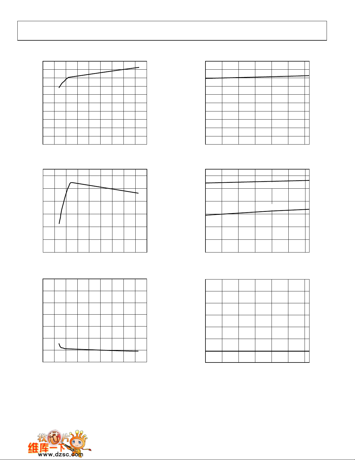
TYPICAL PERFORMANCE CHARACTERISTICS
2.0
1.8
1.6
1.4
1.2
1.0
(mA)
CC
I
0.8
0.6
0.4
0.2
0
024681014112 16
VCC (V)
Figure 4. Supply Current vs. Supply Voltage
8
05647-021
2.0
1.8
1.6
1.4
1.2
1.0
(mA)
CC
I
0.8
0.6
0.4
0.2
0
–40 806040200–20
TEMPERATURE (°C)
Figure 7. Supply Current vs. Temperature (Gate On)
05647-022
12
10
8
6
DRIVE VOLTAGE (V)
4
2
0
01
Figure 5. Drive Voltage (V
0
–2
–4
–6
(µA)
–8
GATE
I
–10
VCC (V)
− VCC) vs. Supply Voltage
GATE
8161412108642
05647-029
12
10
8
6
DRIVE VOLTAGE (V)
4
2
0
–40 806040200–20
Figure 8. Drive Voltage (V
0
–2
–4
–6
(µA)
–8
GATE
I
–10
5V V
3.15V V
TEMPERATURE (°C)
− VCC) vs. Temperature
GATE
CC
CC
05647-030
–12
–14
01
VCC (V)
10 12 16148642
8
05647-027
Figure 6. Gate Pull-Up Current vs. Supply Voltage
–12
–14
–40 806040200–20
Figure 9. Gate Pull-Up Current vs. Temperature
Rev. 0 | Page 8 of 24
TEMPERATURE (°C)
05647-028
 Loading...