

Low Power IEEE 802.15.4 Zero-IF 2.4 GHz
FEATURES
Frequency range (global ISM band)
2400 MHz to 2483.5 MHz
IEEE 802.15.4-2006-compatible (250 kbps)
Low power consumption
19 mA (typical) in receive mode
21.5 mA (typical) in transmit mode (P
1.7 μA, 32 kHz crystal oscillator wake-up mode
High sensitivity
−95 dBm at 250 kbps
Programmable output power
−20 dBm to +4.8 dBm in 2 dB steps
Integrated voltage regulators
1.8 V to 3.6 V input voltage range
Excellent receiver selectivity and blocking resilience
Zero-IF architecture
Complies with EN300 440 Class 2, EN300 328, FCC CFR47
Part 15, ARIB STD-T66
Digital RSSI measurement
Fast automatic VCO calibration
Automatic RF synthesizer bandwidth optimization
= 3 dBm)
O
Transceiver IC
ADF7241
On-chip low power processor performs
Radio control
Packet management
Packet management support
Insertion/detection of preamble address/SFD/FCS
IEEEE 802.15.4-2006 frame filtering
IEEEE 802.15.4-2006 CSMA/CA unslotted modes
Flexible 256-byte transmit/receive data buffer
SPORT mode
Flexible multiple RF port interface
External PA/LNA support hardware
Switched antenna diversity support
Wake -up timer
Very few external components
Integrated PLL loop filter, receive/transmit switch, battery
monitor, temperature sensor, 32 kHz RC and crystal
oscillators
Flexible SPI control interface with block read/write access
Small form factor 5 mm × 5 mm 32-lead LFCSP package
APPLICATIONS
Wireless sensor networks
Automatic meter reading/smart metering
Industrial wireless control
Healthcare
Wireless audio/video
Consumer electronics
ZigBee
FUNCTIONAL BLOCK DIAGRAM
ADF7241
LNA1
LNA2
PA
LDO × 4 BIAS
Rev. 0
Rev. 0
Information furnished by Analog Devices is believed to be accurate and reliable. However, no
Information furnished by Analog Devices is believed to be accurate and reliable. However, no
responsibility is assumed by Anal og Devices for its use, nor for any infringements of patents or ot her
responsibility is assumed by Anal og Devices for its use, nor for any infringements of patents or ot her
rights of third parties that may result from its use. Specifications subject to change without notice. No
rights of third parties that may result from its use. Specifications subject to change without notice. No
license is granted by implication or otherwise under any patent or patent rights of Analog Devices.
license is granted by implication or otherwise under any patent or patent rights of Analog Devices.
Trademarks and registered trademarks are the property of their respective owners.
Trademarks and registered trademarks are the property of their respective owners.
FRACTIONAL-N
RF SYNTHES IZER
BATTERY
MONITOR
DAC
ADC
ADC
DAC
PRE-EMPHASIS FILTER
TEMPERATURE
SENSOR
4kB
PROGRAM
ROM
2kB
PROGRAM
RAM
256-BYTE
PACKET
RAM
64-BYTE
BBRAM
256-BYTE
MCR
SPIWAKE-UP CTRL
GPIO
SPORT
IRQ
09322-001
26MHz
OSC
DSSS
DEMOD
AGC
OCL
CDR
32kHz
RC
OSC
8-BIT
PROCESSOR
RADIO
CONTROLLER
PACKET
MANAGER
32kHz
XTAL
OSC
Figure 1.
One Technology Way, P.O. Box 9106, Norwood, MA 02062-9106, U.S.A.
One Technology Way, P.O. Box 9106, Norwood, MA 02062-9106, U.S.A.
Tel: 781.329.4700 www.analog.com
Tel: 781.329.4700 www.analog.com
Fax: 781.461.3113 ©2011 Analog Devices, Inc. All rights reserved.
Fax: 781.461.3113 ©2011 Analog Devices, Inc. All rights reserved.

ADF7241
TABLE OF CONTENTS
Features.............................................................................................. 1
Applications....................................................................................... 1
Functional Block Diagram .............................................................. 1
Revision History ............................................................................... 2
General Description ......................................................................... 3
Specifications..................................................................................... 5
General Specifications ................................................................. 5
RF Frequency Synthesizer Specifications.................................. 5
Transmitter Specifications........................................................... 6
Receiver Specifications ................................................................ 6
Auxiliary Specifications............................................................... 8
Current Consumption Specifications........................................ 9
Timing and Digital Specifications.............................................. 9
Timing Diagrams........................................................................ 11
Absolute Maximum Ratings.......................................................... 15
ESD Caution................................................................................ 15
Pin Configuration and Function Descriptions........................... 16
Typical Performance Characteristics ........................................... 18
Terminology .................................................................................... 22
Radio Controller............................................................................. 23
Sleep Modes................................................................................. 25
RF Frequency Synthesizer ............................................................. 26
RF Frequency Synthesizer Calibration.................................... 26
RF Frequency Synthesizer Bandwidth..................................... 27
RF Channel Frequency Programming..................................... 27
Reference Crystal Oscillator ..................................................... 27
Transmitter...................................................................................... 28
Transmit Operating Modes....................................................... 28
IEEE 802.15.4 Automatic RX-To-TX Turnaround Mode..... 30
Power Amplifier.......................................................................... 30
Receiver............................................................................................ 33
Receive Operation ...................................................................... 33
Receiver Calibration................................................................... 33
Receive Timing and Control .......................................................35
Clear Channel Assessment (CCA)........................................... 36
Link Quality Indication (LQI).................................................. 36
Automatic TX-to-RX Turnaround Mode ............................... 37
IEEE 802.15.4 Frame Filtering, Automatic Acknowledge, and
Automatic CSMA/CA................................................................ 37
Receiver Radio Blocks ............................................................... 39
SPORT Interface ............................................................................. 40
SPORT Mode .............................................................................. 40
Device Configuration .................................................................... 41
Configuration Values................................................................. 41
RF Port Configurations/Antenna Diversity................................ 42
Auxillary Functions........................................................................ 43
Temperture Sensor..................................................................... 43
Battery Monitor.......................................................................... 43
Wake-Up Controller (WUC).................................................... 43
Transmit Test Modes.................................................................. 44
Serial Peripheral interface (SPI) ................................................... 45
General Characteristics ............................................................. 45
Command Access....................................................................... 45
Status Word ................................................................................. 45
Memory Map .................................................................................. 47
BBRAM........................................................................................ 47
Modem Configuration RAM (MCR) ...................................... 47
Program ROM ............................................................................ 47
Program RAM ............................................................................ 47
Packet RAM ................................................................................ 47
Memory Access............................................................................... 49
Writing to the ADF7241............................................................ 50
Reading from the ADF7241...................................................... 50
Downloadable Firmware Modules............................................... 53
Interrupt Controller....................................................................... 54
Configuration ............................................................................. 54
Description of Interrupt Sources ............................................. 55
Applications Circuits...................................................................... 56
Register Map ................................................................................... 60
Outline Dimensions....................................................................... 71
Ordering Guide .......................................................................... 71
REVISION HISTORY
1/11—Revision 0: Initial Version
Rev. 0 | Page 2 of 72

ADF7241
GENERAL DESCRIPTION
The ADF7241 is a highly integrated, low power, and high performance transceiver for operation in the global 2.4 GHz ISM band. It
is designed with emphasis on flexibility, robustness, ease of use,
and low current consumption. The IC supports the IEEE 802.15.42006 2.4 GHz PHY requirements in both packet and data
streaming modes. With a minimum number of external components, it achieves compliance with the FCC CFR47 Part 15,
ETSI EN 300 440 (Equipment Class 2), ETSI EN 300 328
(FHSS, DR > 250 kbps), and ARIB STD T-66 standards.
The ADF7241 complies with the IEEE 802.15.4-2006 2.4 GHz
PHY requirements with a fixed data rate of 250 kbps and DSSSOQPSK modulation. The transmitter path of the ADF7241 is
based on a direct closed-loop VCO modulation scheme using a
low noise fractional-N RF frequency synthesizer. The
automatically calibrated VCO operates at twice the fundamental
frequency to reduce spurious emissions and avoid PA pulling
effects. The bandwidth of the RF frequency synthesizer is
automatically optimized for transmit and receive operations to
achieve best phase noise, modulation quality, and synthesizer
settling time performance. The transmitter output power is
programmable from −20 dBm to +4 dBm with automatic PA
ramping to meet transient spurious specifications. An
integrated biasing and control circuit is available in the IC to
significantly simplify the interface to external PAs.
The receive path is based on a zero-IF architecture enabling very
high blocking resilience and selectivity performance, which are
critical performance metrics in interference dominated environments such as the 2.4 GHz band. In addition, the architecture
does not suffer from any degradation of blocker rejection in the
image channel, which is typically found in low IF receivers. The
IC can operate with a supply voltage between 1.8 V and 3.6 V with
very low power consumption in receive and transmit modes while
maintaining its excellent RF performance, making it especially
suitable for battery-powered systems.
The ADF7241 features a flexible dual-port RF interface that can
be used with an external LNA and/or PA in addition to supporting switched antenna diversity.
The ADF7241 incorporates a very low power custom 8-bit
processor that supports a number of transceiver management
functions. These functions are handled by the two main modules of the processor: the radio controller and the packet manager.
The radio controller manages the state of the IC in various
operating modes and configurations. The host MCU can use
single byte commands to interface to the radio controller. In
transmit mode, the packet manager can be configured to add
preamble and SFD to the payload data stored in the on-chip
packet RAM. In receive mode, the packet manager can detect
and generate an interrupt to the MCU upon receiving a valid SFD,
and store the received data payload in the packet RAM. A total
of 256 bytes of transmit and receive packet RAM space is
provided to decouple the over-the-air data rate from the host
MCU processing speed. Thus, the ADF7241 packet manager
eases the processing burden on the host MCU and saves the
overall system power consumption.
In addition, for applications that require data streaming, a
synchronous bidirectional serial port (SPORT) provides bitlevel input/output data, and has been designed to directly
interface to a wide range of DSPs, such as ADSP-21xx, SHARC®,
TigerSHARC®, and Blackfin®. The SPORT interface can optionally be used.
The processor also permits the download and execution of a set
of firmware modules, which include IEEE 802.15.4 automatic
modes, such as node address filtering, as well as unslotted
CSMA/CA. Execution code for these firmware modules is
available from Analog Devices, Inc.
To further optimize the system power consumption, the ADF7241
features an integrated low power 32 kHz RC wake-up oscillator,
which is calibrated from the 26 MHz crystal oscillator while the
transceiver is active. Alternatively, an integrated 32 kHz crystal
oscillator can be used as a wake-up timer for applications
requiring very accurate wake-up timing. A battery backed-up
RAM (BBRAM) is available on the IC where IEEE 802.15.42006 network node addresses can be retained when the IC is in
the sleep state.
The ADF7241 also features a very flexible interrupt controller,
which provides MAC-level and PHY-level interrupts to the host
MCU. The IC is equipped with a SPI interface, which allows
burst mode data transfer for high data throughput efficiency.
The IC also integrates a temperature sensor with digital readback and a battery monitor.
Rev. 0 | Page 3 of 72
ADF7241
4kB
PROGRAM
ROM
2kB
PROGRAM
RAM
256- BYTE
PACKET
RAM
64-BYTE
BBRAM
256-BYTE
MCR
SPI
EXT LNA/PA
ENABLE
GPIO
SPORT
IRQ
CS
MOSI
SCLK
MISO
RXEN_GP6
TXEN_GP5
TRCLK_CKO_GP3
DT_GP1
DR_GP0
IRQ1_GP4
IRQ2_TRFS_GP2
RFIO1P
RFIO1N
RFIO2P
RFIO2N
PABIAOP_ATB4
PAVSUP_ATB3
ADF7241
EXT PA
INTERFACE
PA
RAMP
LNA1
LNA2
PA
BATTERY
MONITOR
DIV2 DIVIDER
CHARGE-
PUMP
LOOP FILTER
TEMPERATURE
SENSOR
LDO3LDO2LDO1 BIAS
LDO4
SDM
PFD
ANALOG
TEST
DAC
ADC
ADC
DAC
PRE-EMPHASIS
FILTER
26MHz
OSC
DSSS
DEMOD
AGC
OCL
CDR
DSSS MOD
RC
CAL
8-BIT
PROCESSOR
RADIO
CONTROLLER
PACKET
MANAGER
WAKE-UP CTRL
TIMER UNIT
32kHz
RC
OSC
32kHz
XTAL
OSC
CREGRF1,
CREGRF2,
CREGRF3
CREGDIG1,
CREGDIG2
XOSC32KP_GP7_ATB1XOSC32KN_ATB2XOSC26NXOSC26PRBIASCREGSYNTHCREGVCO
09322-011
Figure 2. Detailed Functional Block Diagram
Rev. 0 | Page 4 of 72

ADF7241
SPECIFICATIONS
VDD_BAT = 1.8 V to 3.6 V, GND = 0 V, TA = T
f
= 2450 MHz. All measurements are performed using the ADF7241 reference design, RFIO2 port, unless otherwise noted.
CHANNEL
GENERAL SPECIFICATIONS
Table 1.
Parameter Min Typ Max Unit Test Conditions
GENERAL PARAMETERS
Voltage Supply Range
VDD_BAT Input 1.8 3.6 V
Frequency Range 2400 2483.5 MHz
Operating Temperature Range −40 +85 °C
Data Rate 250 kbps
RF FREQUENCY SYNTHESIZER SPECIFICATIONS
Table 2.
Parameter Min Typ Max Unit Test Conditions
CHANNEL FREQUENCY RESOLUTION 10 kHz
PHASE ERROR 3 Degrees
1.5 Degrees
VCO CALIBRATION TIME 52 μs Applies to all modes
SYNTHESIZER SETTLING TIME
53 μs Receive mode
80 μs Transmit mode
PHASE NOISE Receive mode
−135 dBc/Hz 10 MHz frequency offset
−145 dBc/Hz ≥50 MHz frequency offset
REFERENCE AND CLOCK-RELATED
SPURIOUS
INTEGER BOUNDARY SPURS 60 dBc
CRYSTAL OSCILLATOR
Crystal Frequency 26 MHz Parallel load resonant crystal
Maximum Parallel Load Capacitance 18 pF
Minimum Parallel Load Capacitance 7 pF
Maximum Crystal ESR 365.3 Ω
Sleep-to-Idle Wake-Up Time 300 μs 15 pF load on XOSC26N and XOSC26P
to T
MIN
70 dBc
, unless otherwise noted. Typical specifications are at VDD_BAT = 3.6 V, TA = 25°C,
MAX
Receive mode; integration bandwidth from 10 kHz
to 400 kHz
Transmit mode; integration bandwidth from 10 kHz
to 1800 kHz
Frequency synthesizer settled to <±5 ppm of the
target frequency within this time following a VCO
calibration
Receive mode; f
2480 MHz
Receive mode; measured at 400 kHz offset from
f
= 2405 MHz, 2418 MHz, 2431 MHz,
CHANNEL
2444 MHz, 2457 MHz, 2470 MHz
Guarantees maximum crystal frequency error of
0.2 ppm; 33 pF on XOSC26P and XOSC26N
= 2405 MHz, 2450 MHz, and
CHANNEL
Rev. 0 | Page 5 of 72

ADF7241
TRANSMITTER SPECIFICATIONS
Table 3.
Parameter Min Typ Max Unit Test Conditions
TRANSMITTER SPECIFICATIONS
Maximum Transmit Power 3 dBm
Minimum Transmit Power −25 dBm
Maximum Transmit Power (High Power
Mode)
Minimum Transmit Power (High Power
Mode)
Transmit Power Variation 2 dB
Transmit Power Control Resolution 2 dB Transmit power = 3 dBm
Optimum PA Matching Impedance 43.7 + 35.2j Ω For maximum transmit power = 3 dBm
Harmonics and Spurious Emissions
Compliance with ETSI EN 300 440
25 MHz to 30 MHz −36 dBm Unmodulated carrier, 10 kHz RBW1
30 MHz to 1 GHz −36 dBm Unmodulated carrier, 100 kHz RBW1
47 MHz to 74 MHz, 87.5 MHz to
118 MHz, 174 MHz to 230 MHz,
470 MHz to 862 MHz
Otherwise Above 1 GHz −30 dBm Unmodulated carrier, 1 MHz RBW1
Compliance with ETSI EN 300 328
1800 MHz to 1900 MHz −47 dBm Unmodulated carrier
5150 MHz to 5300 MHz −97 dBm/Hz
Compliance with FCC CFR47, Part15
4.5 GHz to 5.15 GHz −41 dBm 1 MHz RBW1
7.25 GHz to 7.75 GHz −41 dBm 1 MHz RBW1
Transmit EVM 2 %
Transmit EVM Variation 1 %
Transmit PSD Mask −56 dBm RBW = 100 kHz; |f – f
Transmit 20 dB Bandwidth 2252 MHz
1
RBW = resolution bandwidth.
4.8 dBm
Refer to Power Amplifier section for details on how
to enable this mode
−22 dBm
Transmit power = 3 dBm, f
2483.5 MHz, T
= −40°C to +85°C, VDD_BAT = 1.8 V
A
= 2400 MHz to
CHANNEL
to 3.6 V
−54 dBm Unmodulated carrier, 100 kHz RBW
Measured using Rohde & Schwarz FSU vector
analyzer with Zigbee™ option
= 2405 MHz to 2480 MHz, TA= −40°C to
f
CHANNEL
+85°C, VDD_BAT = 1.8 V to 3.6 V
| > 3.5 MHz
CHANNEL
1
RECEIVER SPECIFICATIONS
Table 4.
Parameter Min Typ Max Unit Test Conditions
GENERAL RECEIVER SPECIFICATIONS
RF Front-End LNA and Mixer IIP3 −13.6 dBm
−12.6 dBm
−10.5 dBm
Rev. 0 | Page 6 of 72
At maximum gain, f
= 10.1 MHz, P
f
BLOCKER2
At maximum gain, f
= 40.1 MHz,
f
BLOCKER2
= −35 dBm
P
RF,IN
At maximum gain, f
= 80.1 MHz,
f
BLOCKER2
P
= −35 dBm
RF,IN
BLOCKER1
= −35 dBm
RF,IN
BLOCKER1
BLOCKER1
= 5 MHz,
= 20 MHz,
= 40 MHz,

ADF7241
Parameter Min Typ Max Unit Test Conditions
RF Front-End LNA and Mixer IIP2 24.7 dBm
RF Front-End LNA and Mixer 1 dB
−20.5 dBm At maximum gain
At maximum gain, f
f
= 5.5 MHz, P
BLOCKER2
Compression Point
Receiver LO Level at RFIO2 Port −100 dBm IEEE 802.15.4 packet mode
LNA Input Impedance at RFIO1x Port 50.2 − 52.2j Ω Measured in RX state
LNA Input Impedance at RFIO2x Port 74.3 − 10.7j Ω Measured in RX state
Receive Spurious Emissions
Compliant with EN 300 440
30 MHz to 1000 MHz −57 dBm
1 GHz to 12.75 GHz −47 dBm
RECEIVE PATH IEEE 802.15.4-2006 MODE
Sensitivity (P
, IEEE 802.15.4) −95 dBm
rf,in,min
1% PER with PSDU length of 20 bytes
according to the IEEE 802.15.4-2006
standard
Saturation Level −15 dBm 1% PER with PSDU length of 20 bytes
CW Blocker Rejection P
RF,IN
= P
, IEEE 802.15.4 + 3 dB
RF,IN,MIN
±5 MHz 55 dB
±10 MHz 60 dB
±20 MHz 63 dB
±30 MHz 64 dB
Modulated Blocker Rejection P
RF,IN
= P
, IEEE 802.15.4 + 3 dB
RF,IN,MIN
±5 MHz 48 dB
±10 MHz 61 dB
±15 MHz 62.5 dB
±20 MHz 65 dB
±30 MHz 65 dB
Co-Channel Rejection −6 dB P
Out-of Band Blocker Rejection
= P
RF,IN
RF,IN,MIN
= P
P
RF,IN
RF,IN,MIN
measured at f
+ 10 dB modulated blocker
, IEEE 802.15.4 + 3 dB,
CHANNEL
−5 MHz −34.2 dBm
−10 MHz −30.7 dBm
−20 MHz −29.7 dBm
−30 MHz −25.7 dBm
−60 MHz −24.2 dBm
= P
P
RF,IN
RF,IN,MIN
measured at f
, IEEE 802.15.4 + 3 dB,
CHANNEL
+5 MHz −33.4 dBm
+10 MHz −29.9 dBm
+20 MHz −28.2 dBm
+30 MHz −23.7 dBm
+60 MHz −29.9 dBm
Receiver Channel Bandwidth 2252 kHz
Two-sided bandwidth; cascaded analog and
digital channel filtering
Frequency Error Tolerance −80 +80 ppm P
RSSI
RF,IN
= P
RF,IN,MIN
+ 3 dB
Measured using IEEE 802.15.4-2006 packet
mode
Dynamic range 85 dB
Accuracy ±3 dB
Averaging Time 128 μs
Minimum Sensitivity −95 dBm
Rev. 0 | Page 7 of 72
= 5 MHz,
BLOCKER1
= −50 dBm
RF,IN
= 2405 MHz
= 2480 MHz

ADF7241
AUXILIARY SPECIFICATIONS
Table 5.
Parameter Min Typ Max Unit Test Conditions
32 kHz RC OSCILLATOR
Frequency 32.768 kHz After calibration
Frequency Accuracy 1 % After calibration at 25°C
Frequency Drift
Temperature Coefficient 0.14 %/°C
Voltage Coefficient 4 %/V
Calibration Time 1 ms
32 kHz CRYSTAL OSCILLATOR
Frequency 32.768 kHz
Maximum ESR 319.8 kΩ 10 pF on XOSC32KP and XOSC32KN
Start-Up Time 2000 ms
WAKE-UP TIMER
Prescaler Tick Period 0.0305 20,000 ms
Wake-Up Period 61 × 10−6 1.31 × 10⁵ sec
TEMPERATURE SENSOR
Range −40 +85 °C
Resolution 4.7 °C
Accuracy ±6.4 °C
BATTERY MONITOR
Trigger Voltage 1.7 3.6 V
Trigger Voltage Step Size 62 mV
Start-Up Time 5 μs
Current Consumption 30 μA
EXTERNAL PA INTERFACE
RON, PAVSUP_ATB3 to VDD_BAT 5 Ω extpa_bias_mode = 0, 1, 2, 5, 6
R
, PAVSUP_ATB3 to GND 10 MΩ extpa_bias_mode = 3, 4, power-down
OFF
R
, PABIASOP_ATB4 to GND 10 MΩ extpa_bias_mode = 0, power-down
OFF
PABIASOP_ATB4 Source Current, Maximum 80 μA expta_bias_mode = 1, 3
PABIASOP_ATB4 Sink Current, Minimum −80 μA extpa_bias_mode = 2, 4
PABIASOP_ATB4 Current Control Resolution 6 Bits extpa_bias_mode = 1, 2, 3, 4, 5
PABIASOP_ATB4 Compliance Voltage 150 mV extpa_bias_mode = 2, 4
PABIASOP_ATB4 Compliance Voltage 3.45 V extpa_bias_mode = 1, 3
Servo Loop Bias Current 22 mA extpa_bias_mode = 5, 6
Servo Loop Bias Current Control Step 0.349 mA extpa_bias_mode = 5, 6
12.5 pF load capacitors on XOSC32KP and
XOSC32KN
Average of 1000 ADC readbacks, after
using linear fitting, with correction at
known temperature
Rev. 0 | Page 8 of 72

ADF7241
CURRENT CONSUMPTION SPECIFICATIONS
Table 6.
Parameter Min Typ Max Unit Test Conditions
CURRENT CONSUMPTION
TX Mode Current Consumption
−20 dBm 16.5 mA IEEE 802.15.4-2006 continuous packet transmission mode
−10 dBm 17.4 mA IEEE 802.15.4-2006 continuous packet transmission mode
0 dBm 19.6 mA IEEE 802.15.4-2006 continuous packet transmission mode
+3 dBm 21.5 mA IEEE 802.15.4-2006 continuous packet transmission mode
+4 dBm 25 mA IEEE 802.15.4-2006 continuous packet transmission mode
Idle Mode 1.8 mA XTO26M + digital active
PHY_RDY Mode 10 mA
RX Mode Current Consumption 19 mA IEEE 802.15.4-2006 packet mode
MEAS State 3 mA
SLEEP_BBRAM 0.3 μA BBRAM contents retained
SLEEP_BBRAM_RCO 1 μA
SLEEP_BBRAM_XTO 1.7 μA
TIMING AND DIGITAL SPECIFICATIONS
32 kHz RC oscillator running, some BBRAM contents
retained, wake-up time enabled
32 kHz crystal oscillator running, some BBRAM contents
retained, wake-up time enabled
Table 7. Logic Levels
Parameter Min Typ Max Unit Test Conditions
LOGIC INPUTS
Input High Voltage, V
Input Low Voltage, V
Input Current, I
Input Capacitance, CIN 10 pF
LOGIC OUTPUTS
Output High Voltage, VOH VDD_BAT − 0.4 V IOH = 500 μA
Output Low Voltage, VOL 0.4 V IOL = 500 μA
Output Rise/Fall 5 ns
Output Load 7 pF
INH/IINL
0.7 × VDD_BAT V
INH
0.2 × VDD V
INL
±1 μA
Table 8. GPIOs
Parameter Min Typ Max Unit Test Conditions
GPIO OUTPUTS
Output Drive Level 5 mA All GPIOs in logic high state
Output Drive Level 5 mA All GPIOs in logic low state
Table 9. SPI Interface Timing
Parameter Min Typ Max Unit Description
t1 15 ns
t2 40 ns
t3 40 ns SCLK high time
t4 40 ns SCLK low time
t5 80 ns SCLK period
t6 10 ns SCLK falling edge to MISO delay
t7 5 ns MOSI to SCLK rising edge setup time
t8 5 ns MOSI to SCLK rising edge hold time
falling edge to MISO setup time (TRX active)
CS
to SCLK setup time
CS
Rev. 0 | Page 9 of 72

ADF7241
Parameter Min Typ Max Unit Description
t9 40 ns
t10 10 ns
t11 270 ns
t12 300 400 μs
t13 20 ns SCLK rise time
t14 20 ns SCLK fall time
t15, t16 2 ms
SCLK to CS
high to SCLK wait time
CS
high time
CS
low to MISO high wake-up time, 26 MHz crystal with 10 pF load capacitance, TA = 25°C
CS
high time on wake-up after RC_RESET or RC_SLEEP command (see and
CS
Figure 31
Table 10. IEEE 802.15.4 State Transition Timing
Parameter Min Typ Max Unit Test Conditions
Idle to PHY_RDY State 142 μs
PHY_RDY to Idle State 13.5 μs
PHY_RDY or TX to RX State (Different Channel) 192 μs VCO calibration performed
PHY_RDY or RX to TX State (Different Channel) 192 μs VCO calibration performed
PHY_RDY or TX to RX State (Same Channel) 140 μs VCO calibration skipped
RX or PHY_RDY to TX State (Same Channel) 140 μs VCO calibration skipped
RX Channel Change 192 μs VCO calibration performed
TX Channel Change 192 μs VCO calibration performed
TX to PHY_RDY State 23 μs
PHY_RDY to CCA State 192 μs
CCA to PHY_RDY State 14.5 μs
RX to Idle State 5.5 μs
TX to Idle State 30.5 μs
Idle to MEAS State 19 μs
MEAS to Idle State 6 μs
CCA to Idle State 14.5 μs
RX to CCA State 18 μs
CCA to RX State 205 μs
hold time
Figure 5
) 26 MHz crystal with 10 pF load
Table 11. Timing IEEE 802.15.4-2006 SPORT Mode
Parameter Min Typ Max Unit Test Conditions/Comments
t21 18 μs SFD detect to TRCLK_CKO_GP3 (data bit clock) active delay
t22 2 μs TRCLK_CKO_GP3 bit period
t23 0.51 μs DR_GP0 to TRCLK_CKO_GP3 falling edge setup time
t24 16 μs TRCLK_CKO_GP3 symbol burst period
t35 1.3 6.2 μs PA nominal power to TRCLK_CKO_GP3 activity/entry into TX state
t36 14 μs RC_PHY_RDY to TRCLK_CKO_GP3 off
t37 10 μs RC_PHY_RDY to PA power shutdown
Table 12. MAC Timing
Parameter Min Typ Max Unit Test Conditions/Comments
t26 38 μs Time from frame received to rx_pkt_rcvd interrupt generation
t27 150 μs
t28 150 μs
t
RX_MAC_DELAY
192 μs IEEE 802.15.4 mode as defined by the standard
Time allowed, from issuing a RC_TX command, to update
Register delaycfg2, Bit mac_delay_ext (0x10B[7:0])
Time allowed, from issuing a RC_TX command, to cancel the RC_TX
command
Rev. 0 | Page 10 of 72
ADF7241
SCLK
TIMING DIAGRAMS
SPI Interface Timing Diagram
CS
t4t
t
MISO
MOSI
t
3
2
t
1
BIT 7 BIT 6 BIT 5 BIT 4 BIT 3 BIT 2 BIT 1 BIT 0 BIT 7 BIT 0 X BIT 7
t
7
7 765432107
5
t
6
t
8
Figure 3. SPI Interface Timing
Additional description and timing diagrams are available in the Serial Peripheral interface section.
Sleep-to-Idle SPI Timing Diagrams
CS
SCLK
MISO
t
12
t
1
76543210
t
6
Figure 4. Sleep-to-Idle State Timing
t
16
t
11
t10t
9
09322-002
t
9
X
09322-003
CS
SPI COMMAND
TO ADF7242
DEVICE STATUS
RC_RESET OR
RC_SLEEP
IDLEIDLE, PHY_RDY, RX SLEEP
09322-064
Figure 5. Wake-Up After an RC_RESET or RC_SLEEP Command
Rev. 0 | Page 11 of 72
ADF7241
MAC Delay Timing Diagram
PACKET
TRANSMITTED
PACKET
RECEIVED
RC_STATUS
REGIST E R irq_src0, FIELD rc_ready
REGISTER irq_sr c1, FIELD rx_pkt_rcvd
REGISTER irq_src1, FIELD tx_pkt_sent
VALID IEEE802.15.4-2006 FRAME
RX TX
tx_mac_dela y +
mac_delay_ext
t
26
t
27,t28
FRAME IN TX_BUFFER
PHY_RDY
09322-016
Figure 6. IEEE 802.15.4 MAC Timing
Rev. 0 | Page 12 of 72
ADF7241
5
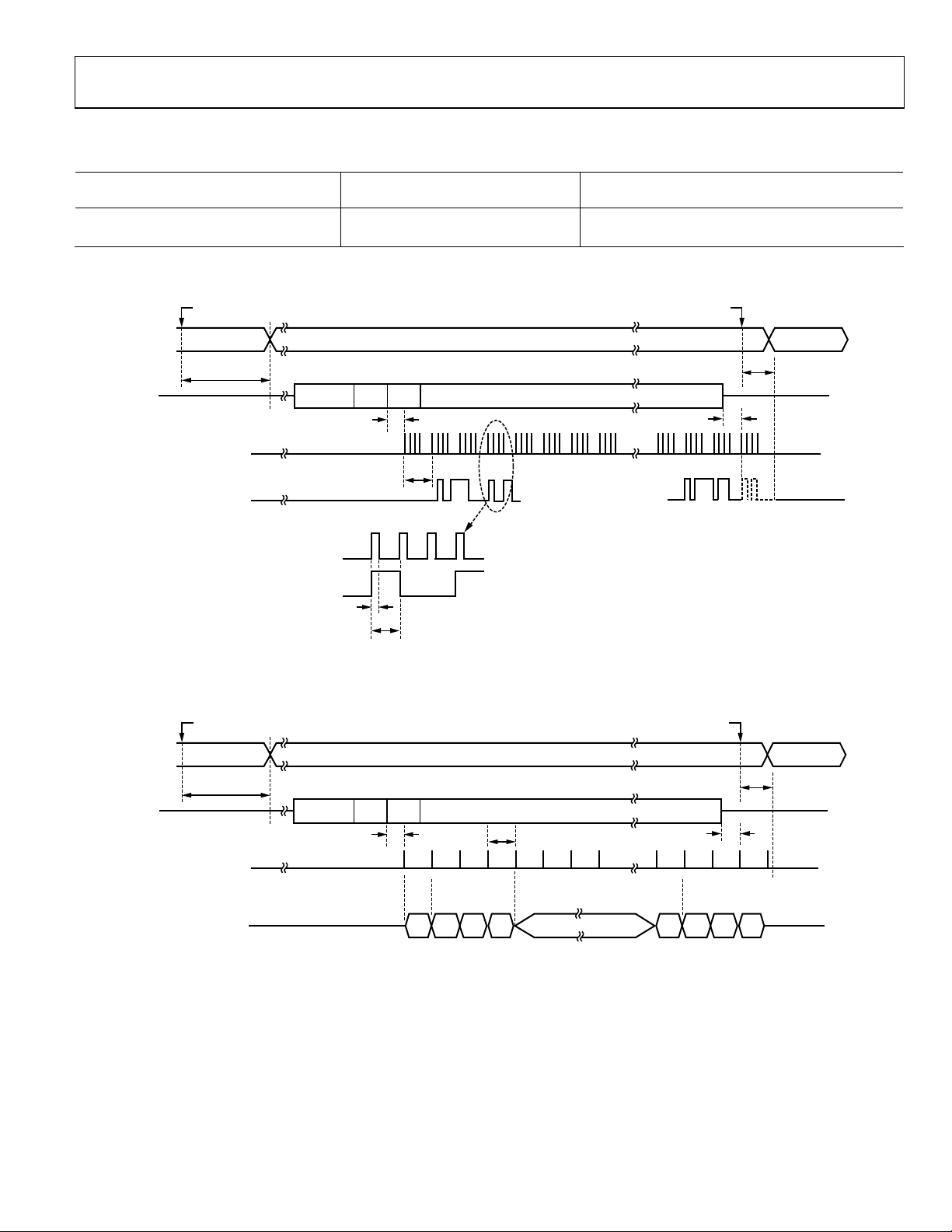
IEEE 802.15.4 RX SPORT Mode Timing Diagrams
Table 13. IEEE 802.15.4 RX SPORT Modes Configurations
Register rc_cfg, Field rc_mode
(0x13E[7:0])
2 1 Bit clock and data available (see Figure 7)
0 7 Symbol clock and data available (see Figure 8)
COMMAND
RC_STATUS
PREVIOUS STATE
t
RX_MAC_DELAY
TRCLK_CKO_GP3
DR_GP0
PREAMBLE SFD PHR PSDU
Register gp_cfg, Field gpio_config
(0x32C[7:0]) Functionality
RC_PHY_RDYRC_RX
RX PHY_RDY
t
29
t
21
t
24
.....
t
21
DATA
INVALID
COMMAND
RC_STATUS
TRCLK_CKO_GP3
GP6, GP5, GP1, GP0
1
GP6 = RXEN_GP6
GP5 = TXEN _G P
GP1 = DT_GP1
GP0 = DR_GP0
TRCLK_CKO_GP3
PREVIOUS STATE
t
RX_MAC_DELAY
1
.....
.....
DR_GP0
.....
.....
t
23
t
22
Figure 7. IEEE 802.15.4 RX SPORT Mode: Bit Clock and Data Available
RX PHY_RDY
PREAMBLE SFD PHR PSDU
SYMBOL
t
21
[3:0]
[3:0]
[3:0]
t
[3:0]
26
Figure 8. IEEE 802.15.4 RX SPORT Mode: Symbol Clock Output
RC_PHY_RDYRC_RX
t
21
[3:0] [3:0]
[3:0] [3:0]
09322-004
t
29
09322-009
Rev. 0 | Page 13 of 72
ADF7241
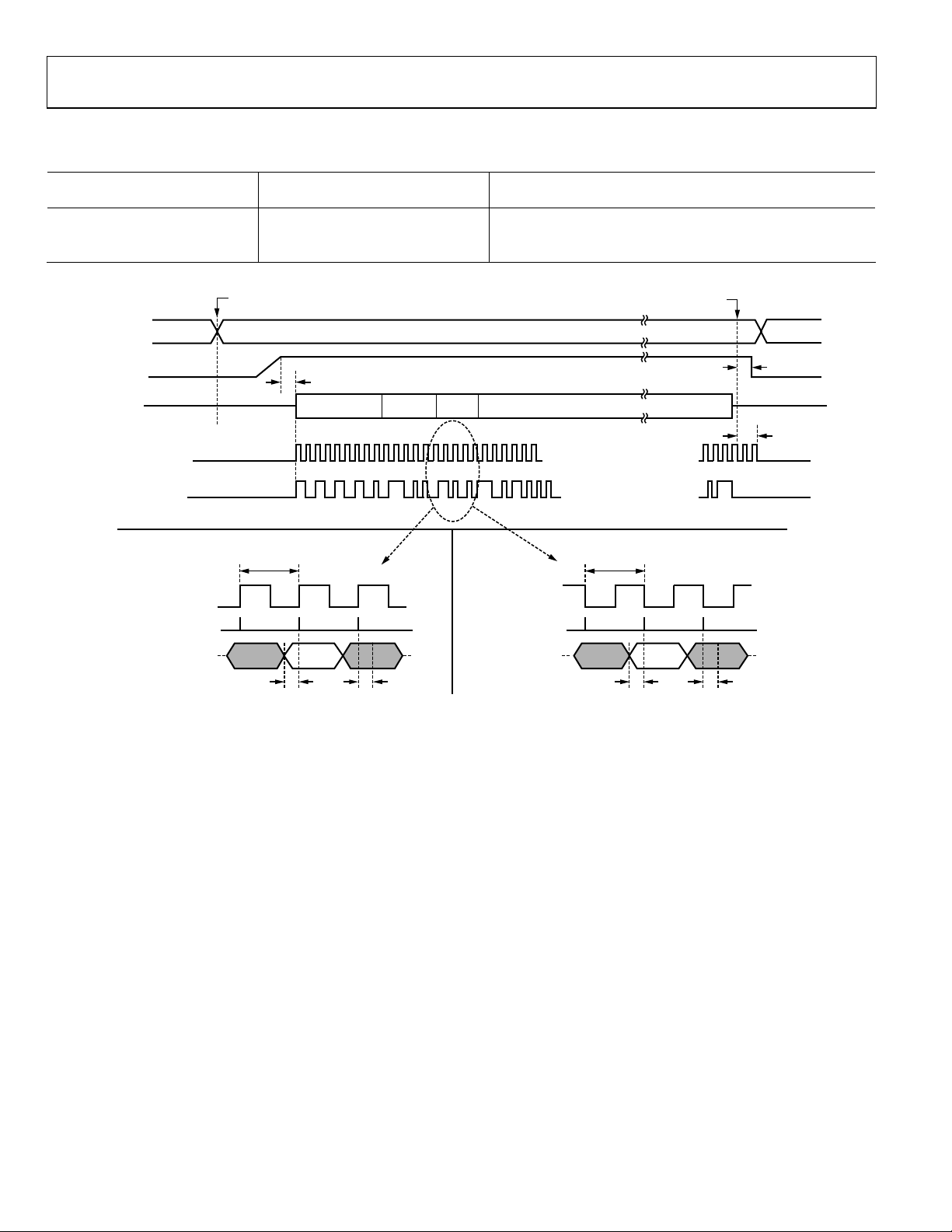
IEEE 802.15.4 TX SPORT Mode Timing Diagram
Table 14. IEE 802.15.4 TX SPORT Mode Configurations
Register rc_cfg, Field rc_mode
(0x13E[7:0])
3 1 or 4 Transmission starts after PA ramp up (see Figure 9)
Register gp_cfg, Field gpio_config
(0x32C[7:0]) Functionality
gpio_config = 1: data clocked in on rising edge of clock
gpio_config = 4: data clocked in on falling edge of clock
RC_TX
RC_PHY_RDY
RC STATE
PA POWER
PACKET
COMPONENT
PHY_RDY
TRCLK_CKO_GP3
DT_GP1
TRCLK_CKO_GP3
DT_GP1 SAM P LE
t
35
PREAMBLE SFD
REGISTER gp_cfg, FIELD gpio_config = 1
DATA CLOCKED IN ON RISING EDGE
DT_GP1
t
32
t
33
Figure 9. IEEE 802.15.4-2006 TX SPORT Mode
Refer to the SPORT Interface section for further details.
TX
PHR
TRCLK_CKO_GP3
DT_GP1 SAM P LE
t
34
PSDU
.....
PACKET DATA
.....
REGISTER gp_cfg, FIELD gpio_config = 4
DATA CLOCKED IN ON FALLING EDG E
DT_GP1
t
32
t
33
PHY_RDY
t
37
t
36
t
34
09322-122
Rev. 0 | Page 14 of 72
ADF7241
ABSOLUTE MAXIMUM RATINGS
TA = 25°C, unless otherwise noted.
Table 15.
Parameter Rating
VDD_BAT to GND −0.3 V to +3.9 V
Operating Temperature Range
Industrial −40°C to +85°C
Storage Temperature Range −65°C to +125°C
Maximum Junction Temperature 150°C
LFCSP θJA Thermal Impedance 26°C/W
Reflow Soldering
Peak Temperature 260°C
Time at Peak Temperature 40 sec
Stresses above those listed under Absolute Maximum Ratings
may cause permanent damage to the device. This is a stress
rating only; functional operation of the device at these or any
other conditions above those indicated in the operational
section of this specification is not implied. Exposure to absolute
maximum rating conditions for extended periods may affect
device reliability.
The exposed paddle of the LFCSP package should be connected
to ground.
This device is a high performance RF integrated circuit with an
ESD rating of <2 kV, and it is ESD sensitive. Proper precautions
should be taken for handling and assembly.
ESD CAUTION
Rev. 0 | Page 15 of 72

ADF7241
PIN CONFIGURATION AND FUNCTION DESCRIPTIONS
PABIAOP_ATB4
PAVSUP_ATB3
VDD_BAT
XOSC32KN_ATB2
XOSC32KP_GP7_ATB1
CREGDIG1
RXEN_GP6
32313029282726
RBIAS
RFIO1P
RFIO1N
RFIO2P
RFIO2N
1
2
3
4
5
6
7
8
ADF7241
TOP VIEW
(Not to Scale)
9
10111213141516
XOSC26P
CREGVCO
VCOGUARD
CREGSYNTH
CREGRF1
CREGRF2
CREGRF3
NOTES
1. THE EXPOSED PADDLE MUST BE CONNECTED TO GRO UND.
Figure 10. Pin Configuration
Table 16. Pin Function Descriptions
Pin No. Mnemonic Description
1 CREGRF1
Regulated Supply Terminal for RF Section. Connect a 220 nF decoupling capacitor from this pin to
GND.
2 RBIAS Bias Resistor 27 kΩ to Ground.
3 CREGRF2 Regulated Supply for RF Section. Connect a 100 pF decoupling capacitor to ground.
4 RFIO1P Differential RF Input Port 1 (Positive Terminal). A 10 nF coupling capacitor is required.
5 RFIO1N Differential RF Input Port 1 (Negative Terminal). A 10 nF coupling capacitor is required.
6 RFIO2P Differential RF Input/Output Port 2 (Positive Terminal). A 10 nF coupling capacitor required.
7 RFIO2N Differential RF Input/Output Port 2 (Negative Terminal). A 10 nF coupling capacitor required.
8 CREGRF3 Regulated Supply for RF Section. Connect a 100 pF decoupling capacitor from this pin to GND.
9 CREGVCO Regulated Supply for VCO Section. Connect a 220 nF decoupling capacitor from this pin to GND.
10 VCOGUARD Guard Trench for VCO Section. Connect to Pin 9 (CREGVCO).
11 CREGSYNTH Regulated Supply for PLL Section. Connect a 220 nF decoupling capacitor from this pin to GND.
12 XOSC26P
Terminal 1 of External Crystal and Loading Capacitor. This pin is no connect (NC) when an external
oscillator is used.
13 XOSC26N Terminal 2 of External Crystal and Loading Capacitor. Input for external oscillator.
14 DGUARD Guard Trench for Digital Section. Connect to Pin 15 (CREGDIG2).
15 CREGDIG2 Regulated Supply for Digital Section. Connect a 220 nF decoupling capacitor to ground.
16 DR_GP0 SPORT Receive Data Output/General-Purpose IO Port.
17 DT_GP1 SPORT Transmit Data Input/General-Purpose IO Port.
18 IRQ2_TRFS_GP2 Interrupt Request Output 2/IEEE 802.15.4-2006 Symbol Clock/General-Purpose IO Port.
19 TRCLK_CKO_GP3 SPORT Clock Output/General-Purpose IO Port.
20 IRQ1_GP4 Interrupt Request Output 1/General-Purpose IO Port.
21 MISO SPI Interface Serial Data Output.
22 SCLK SPI Interface Data Clock Input.
23 MOSI SPI Interface Serial Data Input.
24
CS
SPI Interface Chip Select Input (and Wake-Up Signal).
25 TXEN_GP5 External PA Enable Signal/General-Purpose IO Port.
26 RXEN_GP6 External LNA Enable Signal/General-Purpose IO Port.
27 CREGDIG1 Regulated Supply for Digital Section. Connect a 1 nF decoupling capacitor from this pin to ground.
28 XOSC32KP_GP7_ATB1 Terminal 1 of 32 kHz Crystal Oscillator/General-Purpose IO Port/Analog Test Bus 1.
29 XOSC32KN_ATB2 Terminal 2 of 32 kHz Crystal Oscillator/Analog Test Bus 2.
TXEN_GP5
25
CS
24
23
MOSI
SCLK
22
MISO
21
20
IRQ1_GP4
19
TRCLK_CKO_GP3
18
IRQ2_TRFS_GP2
DT_GP1
17
DR_GP0
DGUARD
XOSC26N
CREGDIG2
09322-010
Rev. 0 | Page 16 of 72

ADF7241
Pin No. Mnemonic Description
30 VDD_BAT Unregulated Supply Input from Battery.
31 PAVSUP_ATB3 External PA Supply Terminal/Analog Test Bus 3.
32 PABIAOP_ATB4 External PA Bias Voltage Output/Analog Test Bus 4.
33 (EPAD) GND Common Ground Terminal. The exposed paddle must be connected to ground.
Rev. 0 | Page 17 of 72
ADF7241
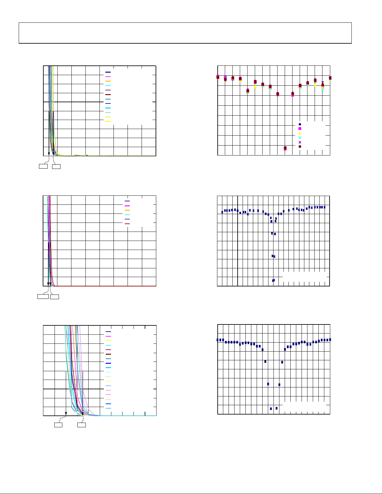
TYPICAL PERFORMANCE CHARACTERISTICS
2.0
1.8
1.6
1.4
1.2
1.0
0.8
0.6
PACKET ERROR RATE (%)
0.4
0.2
0
–100 –90 –80 –70 –60 –50 –40 –30 –20
–96 –93
RF INPUT POWER LEVEL (dBm)
2.405GHz, 1.8V, + 25°C
2.48GHz, 1.8V, +25°C
2.405GHz, 3.6V, + 25°C
2.48GHz, 3.6V, +25°C
2.405GHz, 1.8V, –40°C
2.48GHz, 1.8V, –40°C
2.405GHz, 3.6V, –40°C
2.48GHz, 3.6V, –40°C
2.405GHz, 1.8V, + 85°C
2.48GHz, 1.8V, +85°C
2.405GHz, 3.6V, + 85°C
2.48GHz, 3.6V, +85°C
09322-095
Figure 11. IEEE 802.15.4-2006 Packet Mode Sensitivity vs. Temperature and
VDD_BAT, f
2.0
1.8
1.6
1.4
1.2
1.0
0.8
0.6
PACKET ERROR RATE (%)
0.4
0.2
0
–100 –90 –80 –70 –60 –50 –40 –30 –20
–96.5 –95
= 2.405 GHz, 2.45 GHz, 2.48 GHz, RFIO2x
CHANNEL
RF INPUT POWER LEVEL (dBm)
3.6V, +25°C
1.8V, +25°C
3.6V, –40°C
1.8V, –40°C
3.6V, +85°C
1.8V, +85°C
09322-046
Figure 12. IEEE 802.15.4-2006 Packet Mode PER vs. RF Input Power Level vs.
Temperature and VDD_BAT, f
= 2.45 GHz, RFIO2x
CHANNEL
80
70
60
50
40
30
20
REJECTION LE V EL (d B)
10
0
–10
–45 –40 –35 –30 –25 –20 –15 –10 –5 0 5 10 15 20 25 30
BLOCKER FREQ UE NCY OFFSET (MHz)
1.8V, +25°C
3.6V, +25°C
1.8V, –40° C
3.6V, –40° C
1.8V, +85°C
3.6V, +85°C
09322-048
Figure 14. IEEE 802.15.4-2006 Packet Mode Blocker Rejection vs. Temperature
and VDD_BAT, Modulated Blocker, P
f
= 2.45 GHz, RFIO2x
CHANNEL
80
70
60
50
40
30
20
10
0
BLOCKER REJECTION LEVEL (dB)
–10
–20
–110 –90 –70 –50 –30 –10 10 50 70 90 110
BLOCKER FRE QUENCY OFFSET (MHz )
= −85 dBm + 3 dB,
WANTED
VDD_BAT = 3.6V
TEMPERAT URE = 25°C
09322-049
Figure 15. IEEE 802.15.4-2006 Packet Mode Wide-Band Blocker Rejection,
CW Blocker, P
= −95 dBm + 3 dB, f
WANTED
= 2.45 GHz, RFIO2x
CHANNEL
2.0
1.8
1.6
1.4
1.2
1.0
0.8
0.6
PACKET ERROR RATE (%)
0.4
0.2
0
–100 –98 –96
–94 –92 –90 –88 –86 –84 –82 –80
–96 –93
RF INPUT POWER LEVEL (dBm)
2.405GHz, 1.8V, +25°C
2.450GHz, 1.8V, +25°C
2.475GHz, 1.8V, +25°C
2.405GHz, 3.6V, +25°C
2.450GHz, 3.6V, +25°C
2.475GHz, 3.6V, +25°C
2.405GHz, 1.8V, –40°C
2.450GHz, 1.8V, –40°C
2.475GHz, 1.8V, –40°C
2.405GHz, 3.6V, –40°C
2.450GHz, 3.6V, –40°C
2.475GHz, 3.6V, –40°C
2.405GHz, 1.8V, +85°C
2.450GHz, 1.8V, +85°C
2.475GHz, 1.8V, +85°C
2.405GHz, 3.6V, +85°C
2.450GHz, 3.6V, +85°C
2.475GHz, 3.6V, +85°C
Figure 13. IEEE 802.15.4 Packet Mode Sensitivity vs. Temperature and
VDD_BAT, f
= 2.405 GHz, 2.45 GHz, 2.475 GHz, RFIO1x
CHANNEL
09322-047
Rev. 0 | Page 18 of 72
80
70
60
50
40
30
20
10
0
BLOCKER REJECTION LEVE L (dB)
–10
–20
–20 –16 –12 –8 –4 0 4 8 12 16 20
BLOCKER FREQ UE NCY OFFSET (MHz)
VDD_BAT = 3.6V
TEMPERATURE = 2 5° C
Figure 16. IEEE 802.15.4 Packet Mode Narrow-Band Blocker Rejection,
CW Blocker, P
= −95 dBm + 3 dB, f
WANTED
= 2.45 GHz, RFIO2x
CHANNEL
09322-050
ADF7241
–
80
70
60
50
40
30
20
1.8V, +25° C
3.6V, +25° C
10
1.8V, –40°C
BLOCKER REJECT ION LEVE L (dB)
3.6V, –40°C
1.8V, +85° C
0
3.6V, +85° C
–10
–45 –40 –35 –30 –25 –20 –15 –10 –5 0 5 10 15 20 25 30
BLOCKER FREQ UE NCY OFFSET (MHz)
Figure 17. IEEE 802.15.4 Packet Mode Wide-Band Blocker Rejection vs.
Temperature and VDD_BAT, Modulated Blocker, P
= 2.45 GHz, RFIO2x
f
CHANNEL
80
70
60
50
40
30
20
REJECTION LEVEL (dB)
1.8V, +25°C
3.6V, +25°C
10
1.8V, –40° C
3.6V, –40° C
1.8V, +85°C
0
3.6V, +85°C
–10
–20 –16 –12 –8 –4 0 4 8 12 16 20
INTERFERER FREQUENCY OFFSET (MHz)
= −95 dBm + 3 dB,
WANTED
Figure 18. IEEE 802.15.4 Packet Mode Narrow-Band Blocker Rejection vs.
Temperature and VDD_BAT, Modulated Blocker, P
= 2.45 GHz, RFIO2x
f
CHANNEL
20
CHANNEL 2.405G Hz
CHANNEL 2.48G Hz
–22
–24
–26
–28
–30
–32
BLOCKER REJE CTION L E VEL (dBm)
–34
–36
–110 –90 –70 –50 –30 –10 10 30 50 70 90 110
BLOCKER FREQUENCY OF FSET (MHz )
= −95 dBm + 3 dB,
WANTED
Figure 19. IEEE 802.15.4 Packet Mode Out-of-Band Blocker Rejection,
CW Blocker, P
= −95 dBm + 3 dB, f
WANTED
= 2.405 GHz and 2.48 GHz,
CHANNEL
RFIO2x, VDD_BAT = 3.6 V, Temperature = 25°C
09322-099
09322-100
09322-101
6
MAX 1.8V, + 25°C
5
MIN 1.8V, + 25°C
MAX 3.6V, + 25°C
4
MIN 3.6V, + 25°C
3
2
1
0
–1
–2
RSSI ERROR (dB)
–3
–4
–5
–6
–95 –90 –85 –80 –75 –70 –65 –60 –55 –50 –45 –40 –35 –30 –25 –20
RF INPUT LEVEL (dBm)
MAX 1.8V, –40° C
MIN 1.8V, –40°C
MAX 3.6V, –40° C
MIN 3.6V, –40°C
MAX 1.8V, +85° C
MIN 1.8V, + 85°C
MAX 3.6V, +85° C
MIN 3.6V, + 85°C
09322-112
Figure 20. IEEE 802.15.4 Packet Mode RSSI Error vs. RF Input Power Level vs.
Temperature and VDD_BAT, f
275
250
225
200
175
150
125
100
75
SQI READBACK VALUE
50
25
0
–95–100 –90 –85 –80 –75 –70 –65 –60 –55 –50 –45 –40 –35 –30 –25–20
MAX 1.8V, +25°C
MAX 3.6V, +25°C
MAX 1.8V, –4 0°C
MAX 3.6V, –4 0°C
MAX 1.8V, +85°C
MAX 3.6V, +85°C
RF INPUT LEVEL (dBm)
= 2.45 GHz, RFIO2x
CHANNEL
MIN 1.8V, + 25°C
MIN 3.6V, + 25°C
MIN 1.8V, –40°C
MIN 3.6V, –40°C
MIN 1.8V, + 85°C
MIN 3.6V, + 85°C
09322-113
Figure 21. IEEE 802.15.4 Packet Mode SQI vs. RF Input Power Level vs.
Temperature and VDD_BAT, f
110
100
90
80
70
60
50
40
30
CCA DETECTION RATE (%)
20
10
0
–90 –15–85 –80 –75 –70 –65 –60 –55 –50 –45 –40 –35 –30 –25 –20
–80
dBm
–90
dBm
–70
dBm
THRESHOLD =
–50
–60
dBm
dBm
RF INPUT POWER LEVE L (dBm)
= 2.45 GHz, RFIO2x
CHANNEL
–30
–40
dBm
dBm
–20
dBm
09322-114
Figure 22. IEEE 802.15.4-2006 CCA Operation vs. RSSI Threshold,
= 2.45 GHz, VDD_BAT = 3.6 V, Temperature = 25°C, RFIO2x
f
CHANNEL
Rev. 0 | Page 19 of 72
ADF7241
0
–10
–20
–30
–40
–50
–60
TRANSMITTER RF OUTPUT P OWER (dBm)
–70
–5 –4 –3 –2 –1 0 1 2 3 4 5
FREQUENCY ERROR (kHz)
1.8V, +25° C
3.6V, +25° C
1.8V, –40°C
3.6V, –40°C
1.8V, +85° C
3.6V, +85° C
09322-104
Figure 23. IEEE 802.15.4-2006 Transmitter Spectrum vs. Temperature and
VDD_BAT, f
2.5
2.4
2.3
2.2
2.1
2.0
1.9
1.8
1.7
1.6
1.5
1.4
1.3
1.2
1.1
TRANSMIT T E R E RRO R VE CT OR MAGNIT UDE (%)
1.0
2405 2415 2425 2435 2445 2455 2465 2475
= 2.45 GHz, Output Power = 3 dBm
CHANNEL
CHANNEL FREQUENCY (MHz)
EVM 1.8V , +25°C
EVM 3.6V , +25°C
EVM 1.8V , –40°C
EVM 3.6V , –40°C
EVM 1.8V , +85°C
EVM 3.6V , +85°C
09322-105
Figure 24. IEEE 802.15.4-2006 Transmitter EVM vs. Temperature and
VDD_BAT at All Channels, Output Power = 3 dBm
4.0
3.5
3.0
2.5
2.0
1.5
1.0
PA OUTPUT POWER LEVEL (dBm)
0.5
0
2.40 2.41 2.42 2.43 2.44 2.45 2.46 2.47 2.48
FREQUENCY (GHz )
3.6V, +85°C
3.6V, +25°C
3.6V, –40° C
1.8V, –40° C
1.8V, +25°C
1.8V, +80°C
09322-110
Figure 25. PA Output Power vs. RF Carrier Frequency, Temperature, and VDD_BAT
(A discrete matching network and a harmonic filter are used as per the
ADF7241 reference design.)
4
2
0
–2
–4
–6
–8
–10
–12
–14
–16
–18
–20
–22
PA OUTPUT POWER LEVEL (dBm)
–24
–26
–28
3 4 5 6 7 8 9 101112131415
PA LEVEL SETTING
3.6V, +85°C
3.6V, +25°C
3.6V, –40° C
1.8V, –40° C
1.8V, +25°C
1.8V, +80°C
09322-111
Figure 26. PA Output Power vs. Control Word, Temperature, and VDD_BAT,
= 2.44 GHz (A discrete matching network and a harmonic filter are
f
CHANNEL
used as per the ADF7241 reference design.)
5.0
2.5
0
–2.5
–5.0
–7.5
–10.0
–12.5
–15.0
–17.5
–20.0
–22.5
TRANSMITTER OUTPUT POWER (dBm)
–25.0
–27.5
345678910111213141516
POWER AMPLIF I E R CONT RO L W O RD
HIGH POWER MODE
DEFAULT MODE
09322-119
Figure 27. Transmitter Output Power vs. Control Word for Default and High
Power Modes, f
= 2.45 GHz, VDD_BAT = 3.6 V, Temperature = 25°C,
CHANNEL
RF Carrier Frequency, Temperature, and VDD_BAT
(A discrete matching network and a harmonic filter are used as per the
ADF7241 reference design.)
26.0
25.5
25.0
24.5
24.0
23.5
23.0
22.5
22.0
21.5
21.0
20.5
20.0
19.5
19.0
18.5
18.0
17.5
17.0
16.5
TRANSMI T TER CURRENT CONSUMPT ION (mA)
16.0
3 4 5 6 7 8 9 10 11 12 13 14 15
HIGH POWER MO DE
DEFAULT MODE
POWER AMPLIFIER CONTROL WORD
09322-120
Figure 28. Transmitter Current Consumption vs. Control Word, for Default
and High Power Modes, f
= 2.45 GHz, VDD_BAT = 3.6 V,
CHANNEL
Temperature = 25°C
Rev. 0 | Page 20 of 72

ADF7241
85
3-SIGMA TEMPERATURE E RROR
80
75
TEMPERAT URE READING (L INEAR FIT TING)
70
TEMPERAT URE READING
65
(POLYNOMIAL FITTING)
60
55
50
45
40
35
30
25
20
15
10
5
0
–5
FROM ADC READING (°C)
–10
TEMPERAT URE CAL CUL ATED
–15
–20
–25
–30
–35
–40
–40 –30 –20 –10 0 10 20 30 40 50 60 70 80
TEMPERATUR E (°C)
Figure 29. Temperature Sensor Performance
(Average of 1000 ADC Readbacks) and 3-∑ Error vs. Temperature,
VDD_BAT = 3.6 V
09322-116
Rev. 0 | Page 21 of 72

ADF7241
TERMINOLOGY
ACK
IEEE 802.15.4-2006 acknowledgment frame
ADC
Analog-to-digital converter
AGC
Automatic gain control
Battmon
Battery monitor
CCA
Clear channel assessment
BBRAM
Backup battery random access memory
CSMA/CA
Carrier-sense-multiple-access with collision avoidance
DR
Data rate
DSSS
Direct sequence spread spectrum
FCS
Frame check sequence
FHSS
Frequency hopping spread spectrum
FCF
Frame control field
LQI
Link quality indicator
MCR
Modem configuration register
MCU
Microcontroller unit
NC
Not connected
OCL
Offset correction loop
OQPSK
Offset-quadrature phase shift keying
PA
Power amplifier
PHR
PHY header
PHY
Physical layer
POR
Power-on reset
PSDU
PHY service data unit
RC
Radio controller
RCO32K
32 kHz RC oscillator
RSSI
Receive signal strength indicator
RTC
Real-time clock
SFD
Start-of-frame delimiter
SQI
Signal quality indicator
VCO
Voltage-controlled oscillator
WUC
Wak e -u p co nt r ol le r
XTO26M
26 MHz crystal oscillator
XTO32K
32 kHz crystal oscillator
Rev. 0 | Page 22 of 72

ADF7241
RADIO CONTROLLER
COLD START
(BATTERY APP L I E D)
CONFIG URE DE VICE
FIRMWARE DOWNLOAD
FOR EXAMPLE, IEEE 802.15.4 AUTO-MODES
WUC TIMEOUT
R
C
_
I
D
L
E
RC_TX
MEAS
TX
RC_MEAS
RC_IDLE
K
C
A
P
IDLE
E
L
D
I
_
C
R
RC_PHY_RDY
CCA COMPLETE
PHY_RDY
Y
D
R
_
Y
H
P
_
C
R
T
E
X
T
_
C
R
1
D
TTE
I
M
S
N
A
TR
RC_TX
RC_RX
CS
RC_SLEEP
R
C
_
I
D
L
E
RC_PHY_RDY
RC_CCA
R
C
R
C
_
R
X
PA
C
K
ET
SLEEP
RC_SLEEP
(FROM ANY STATE)
RC_RESET
(FROM ANY STATE)
CCA
C
C
A
C
O
M
P
LE
_
P
H
Y
_
R
D
Y
R
EC
EIVED
R
R
C
_
R
X
1
TE
C
_
C
C
A
E
IDL
RC_
RX
RC_RX
AUTO_RX_TO_TX_TURNAROUND
AUTO_TX_TO_RX_TURNAROUND
1
AVAILABLE IN PACKET MODE.
2
THESE TRANS ITIO NS ARE CONFIGURED IN BUFFERCFG (0x10 7[ 3: 2]).
KEY
STATE T RANS ITION INITIATED BY HOST MCU
AUTOMATI C STATE TRANSI T ION INITIATED BY RADI O CO NT ROLLER
RADIO STAT E
2
2
09322-024
Figure 30. State Diagram
Rev. 0 | Page 23 of 72

ADF7241
The ADF7241 incorporates a radio controller that manages the
state of the IC in various operating modes and configurations.
The host MCU can use single-byte commands to interface to
the radio controller. The function of the radio controller
includes the control of the sequence of powering up and
powering down various blocks as well as system calibrations in
different states of the device. Figure 30 shows the state diagram
of the ADF7241 with possible transitions that are initiated by
the host MCU and automatically by the radio controller.
Device Initialization
When the battery voltage is first applied to the ADF7241, a cold
start-up sequence should be followed, as shown in Figure 31.
The start-up sequence is as follows:
• Apply the battery voltage, VDD_BAT, to the device with
the desired voltage ramp rate. After a time, t
RAMP
,
VDD_BAT reaches its final voltage value.
• After t
, execute the SPI command, RC_RESET. This
RAMP
command resets and shuts down the device.
• After the specified time, t
, the host MCU can set the CS
15
port of the SPI low.
• Wait until the MISO output of the SPI (SPI_READY flag)
goes high, at which time the device is in the idle state and
ready to accept commands.
A power-on reset takes place when the host MCU sets the
CS
port of the SPI low. All device LDOs are enabled together with
the 26 MHz crystal oscillator and the digital core. After the
radio controller initializes the configuration registers to their
default values, the device enters the idle state.
The cold start-up sequence is needed only when the battery
voltage is first applied to the device. Afterwards, a warm startup sequence can be used where the host MCU can wake up the
device from a sleep state by setting the
CS
port of the SPI low.
Idle State
In this state, the receive and transmit blocks are powered down.
The digital section is enabled and all configuration registers, as
well as the packet RAM, are accessible. The host MCU must set
any configuration parameters, such as modulation scheme,
channel frequency, and WUC configuration, in this state.
Bringing the
CS
input low in the sleep state causes a transition
into the idle state. The transition from the sleep state to the idle
state timing is shown in . The idle state can also be
Figure 4
entered by issuing an RC_IDLE command in any state other
than the sleep state.
PHY_RDY State
Upon entering the PHY_RDY state from the idle state, the RF
frequency synthesizer is enabled and a system calibration is
carried out. The receive and transmit blocks are not enabled
in this state. The system calibration is omitted when the
PHY_RDY state is entered from the RX, TX, or CCA state.
The PHY_RDY state can be entered from the idle, RX, TX, or
CCA state by issuing an RC_PHY_RDY command.
RX State
The RF frequency synthesizer is automatically calibrated to the
programmed channel frequency upon entering the RX state from
the PHY_RDY or TX state. The frequency synthesizer calibration can be omitted for single-channel communication systems
if short turnaround times are required. Following a programmable
MAC delay period, the ADF7241 starts searching for a preamble
and a synchronization word if enabled by the user.
The RX state can be entered from the PHY_RDY, CCA, and TX
states by issuing an RC_RX command. Depending on whether
the device is configured to operate in packet or SPORT mode by
setting Register buffercfg, Field rx_buffer_mode, the device can
revert automatically to the PHY_RDY state when a packet is
received, or remain in the RX state until a command to enter a
different state is issued. Refer to the Receiver section for further
details.
CCA State
Upon entering the CCA state, a clear channel assessment is
performed. The CCA state can be entered from the PHY_RDY
or RX state by issuing an RC_CCA command. By default, upon
completion of the clear channel assessment, the ADF7241
automatically reverts to the state from which the RC_CCA
command originated.
TX State
Upon entering the TX state, the RF frequency synthesizer is
automatically calibrated to the programmed channel frequency.
The frequency synthesizer calibration can be omitted for
communication systems operating on a single channel if short
turnaround times are required. Following a programmable
delay period, the PA is ramped up and transmission is initiated.
The TX state can be entered from the PHY_RDY or RX state by
issuing the RC_TX command. Depending on whether the
device is configured to operate in packet or SPORT mode by
setting Register buffercfg, Field rx_buffer_mode, the device can
revert automatically to the PHY_RDY state when a packet is
transmitted, or remain in the TX state until a command to enter
a different state is issued. Refer to the Tra ns m it te r section for
further details.
MEAS State
The MEAS state is used to measure the chip temperature. The
transmitter and receiver blocks are not enabled in this state. The
chip temperature is measured using the ADC, which can be
read from Register adc_rbk, Field adc_out, and is continuously
updated with the chip temperature reading.
This state is enabled by issuing the RC_MEAS command from the
idle state and can be exited using the RC_IDLE command.
Rev. 0 | Page 24 of 72

ADF7241
Sleep States SLEEP_BBRAM_XTO
The sleep state is entered with the RC_SLEEP command. The
sleep state can be configured to operate in three different
modes, which are listed in Tab l e 1 7 .
Table 17. ADF7241 Sleep Modes
Sleep Mode
SLEEP_BBRAM BBRAM Packet RAM and modem
SLEEP_BBRAM_XTO BBRAM and
SLEEP_BBRAM_RCO BBRAM and
1
Refer to the Receiver Configuration in Packet Mode section for further
details.
Active
Circuits
32 kHz
crystal
oscillator
32 kHz RC
Oscillator
Functionality
configuration register (MCR)
contents are not maintained.
BBRAM retains the IEEE
802.15.4-2006 node
addresses
32 kHz crystal oscillator is
enabled, with data retention
in the BBRAM.
32 kHz RC oscillator is
enabled, with data retention
in the BBRAM.
1
.
SLEEP MODES
The sleep modes are configurable with the wake-up configuration registers, tmr_cfg0 and tmr_cfg1. The contents of Register
tmr_cfg0 and Register tmr_cfg1 are reset in the sleep state.
SLEEP_BBRAM
This mode is suitable for applications where the MCU is equipped
with its own wake-up timer. SLEEP_BBRAM mode is enabled
by setting Register tmr_cfg1, Field sleep_config = 1.
APPLY
VDD_BAT
This mode enables the 32 kHz crystal oscillator and retains
certain configuration registers in the BBRAM during the sleep
state. To enable SLEEP_BBRAM_XTO mode, set Register
tmr_cfg1, Field sleep_config = 5. A wake-up interrupt can be
set using, for example, Register irq1_en0, Field wakeup = 1.
Refer to the Wak e -Up C on t ro l le r ( WU C ) section for details on
how to configure the ADF7241 WUC.
SLEEP_BBRAM_RCO
This mode enables the 32 kHz RC oscillator and retains certain
configuration registers in the BBRAM during the sleep state.
This mode can be used when lower timer accuracy is acceptable
by the communication system. It is enabled by setting Register
tmr_cfg1, Field sleep_config = 11. A wake-up interrupt can be
set using, for example, Register irq1_en0, Field wakeup = 1.
Refer to the Wak e -Up C on t ro l le r ( WU C ) section for details on
how to configure the ADF7241 WUC.
Wake-Up from the Sleep State
The host MCU can bring CS low at any time to wake the
CS
ADF7241 from the sleep state. After bringing
low, it must
wait until the MISO output (SPI_READY flag) goes high prior
to accessing the SPI port. This delay reflects the start-up time of
the ADF7241. When the MISO output is high, the voltage
regulator of the digital section and the crystal oscillator have
stabilized. Unless the chip is in the sleep state, the MISO pin
always goes high immediately after bringing
CS
low. The sleep
state can also be exited by a timeout event with the WUC
configured. Refer to the section
Wake -Up C ont r ol l er ( WU C )
for details on how to configure the ADF7241 WUC.
t
15
CS
SPI COMM AND
TO ADF7241
DEVICE STATE
Figure 31. Cold Start Sequence from Application of the Battery
RC_RESET
(0xC8)
IDLEIDLE SLEEP
09322-063
Rev. 0 | Page 25 of 72

ADF7241
RF FREQUENCY SYNTHESIZER
A fully integrated RF frequency synthesizer is used to generate
both the transmit signal and the receive LO signal. The architecture of the frequency synthesizer is shown in Figure 32. The
receiver uses the frequency synthesizer circuit to generate the
local oscillator (LO) for downconverting an RF signal to the
baseband. The transmitter is based on a direct closed-loop VCO
modulation scheme using a low noise fractional-N RF frequency synthesizer, where a high resolution Σ-Δ modulator is
used to generate the required frequency deviations at the RF in
response to the data being transmitted.
The VCO and the frequency synthesizer loop filter of the ADF7241
are fully integrated. To reduce the effect of VCO pulling by the
power-up of the power amplifier, as well as to minimize spurious
emissions, the VCO operates at twice the RF frequency. The
VCO signal is then divided by 2 giving the required frequency
for the transmitter and the required LO frequency for the receiver.
The frequency synthesizer also features automatic VCO calibration and bandwidth selection.
RX AND TX
CIRCUITS
DIV2
VCO
CALIBRATION
N-DIVIDER
CHARGE-PUMP
AND
LOOP FILTER
AUTO SYNTH
BANDWIDTH
SELECTION
Figure 32. Synthesizer Architecture
SDM
PFD
CHANNEL SE LECTI ON
IN RX OR TX
26MHz XOSC
+ DOUBLER
RF FREQUENCY SYNTHESIZER CALIBRATION
The ADF7241 requires a system calibration prior to being
used in the RX, CCA, or TX state. Because the calibration
information is reset when the ADF7241 enters a sleep state, a
full system calibration is automatically performed on the
transition between the idle and PHY_RDY states. The system
calibration is omitted when the PHY_RDY state is entered from
the TX, RX, or CCA state.
142µs
PWR Up RC Cal VCO Cal
24µs 20µs 52µs 46µs
SET REGISTER vco_cal_cfg, FIELD skip_vco_cal = 9
Figure 33. System Calibration Following RC_PHY_RDY
DO NOT SKIP,
Figure 33 shows a breakdown of the total system calibration
time. It comprises a power-up delay, calibration of the receiver
baseband filter (RC Cal), and a VCO calibration (VCO Cal). Once
the VCO is calibrated, the frequency synthesizer is allowed to
settle to within ±5 ppm of the target frequency. A fully automatic fast VCO frequency and amplitude calibration scheme is
SYNTHESIZER
SETTLING
09322-012
09322-089
used to mitigate the effect of temperature, supply voltage, and
process variations on the VCO performance.
The VCO calibration phase must not be skipped during the system
calibration in the PHY_RDY state. Therefore, it is important to
ensure that Register vco_cal_cfg, Field skip_vco_cal = 9 prior to
entering the PHY_RDY state from the idle state. This is the
default setting and, therefore, only requires programming if
skipping of the calibration was previously selected.
The VCO calibration can be skipped on the transition from the
PHY_RDY state to the RX, TX, and CCA states on the condition that the calibration has been performed in the PHY_RDY
state on the same channel frequency to be used in the RX, TX,
and CCA states. The following sequence should be used if
skipping the VCO calibration is required in any state following
the PHY_RDY state:
1. After the system calibration is performed in the PHY_RDY
state, the VCO frequency band in Register vco_band_rb,
Field vco_band_val_rb and the VCO bias DAC code in
Register vco_idac_rb, Field vco_idac_val_rb should be read
back.
2. Before transitioning to any other state and assuming
operation on the same channel frequency, the VCO
frequency band and amplitude DAC should be overwritten
as follows:
a) Set Register vco_cal_cfg, Field skip_vco_cal = 15 to
skip the VCO calibration.
b) Enable the VCO frequency over-write mode by setting
Register vco_ovrw_cfg, Field vco_band_ovrw_en = 1.
c) Write the VCO frequency band read back after the
system calibration in the PHY_RDY state to Register
vco_band_ovrw, Field vco_band_ovrw_val.
d) Enable the VCO bias DAC over-write mode by setting
Register vco_ovrw_cfg, Field vco_idac_ovrw_en = 1
e) Write the VCO bias DAC read back after the system
calibration in the PHY_RDY state to Register
vco_idac_ovrw, Field vco_idac_ovrw_val .
Following the preceding procedure, the device can transition
to other states, which use the same channel frequency without
performing a VCO calibration. If it is required to change the
channel frequency before entering the RX, TX, or CCA state at any
point after the preceding procedure has been used, Register vco_
cal_cfg, Field skip_vco_cal must be set to 9 before transitioning
to the respective state. Then the VCO calibration is automatically performed.
Rev. 0 | Page 26 of 72

ADF7241
RF FREQUENCY SYNTHESIZER BANDWIDTH
The ADF7241 radio controller optimizes the RF frequency synthesizer bandwidth based on whether the device is in the RX or the
TX state. If the device is in the RX state, the frequency synthesizer bandwidth is set by the radio controller to ensure optimum
blocker rejection. If the device is in the TX state, the radio
controller sets the frequency synthesizer bandwidth based on
the required data rate to ensure optimum modulation quality.
RF CHANNEL FREQUENCY PROGRAMMING
The frequency of the synthesizer is programmed with the
frequency control word, ch_freq[23:0], which extends over
Register ch_freq0, Register ch_freq1, and Register ch_freq2.
The frequency control word, ch_freq[23:0], contains a binary
representation of the absolute frequency of the desired channel
divided by 10 kHz.
Writing a new channel frequency value to the frequency control
word, ch_freq[23:0], takes effect after the next frequency synthesizer calibration phase. The frequency synthesizer is calibrated
by default during the transition into the PHY_RDY from the
idle state as well as in the TX, RX and CCA states. Refer to the
RF Frequency Synthesizer Calibration, Transmitter, and
Receiver sections for further details. To facilitate fast channel
frequency changes, a new frequency control word can be
written in the RX state before a packet has been received. The
next RC_RX or RC_TX command initiates the required
frequency synthesizer calibration and settling cycle. Similarly, a
new frequency control word can be written after a packet has
been transmitted while in the TX state and the next RC_RX or
RC_TX command initiates the frequency synthesizer
calibration and settling cycle.
REFERENCE CRYSTAL OSCILLATOR
The on-chip crystal oscillator generates the reference frequency
for the frequency synthesizer and system timing. The oscillator
operates at a frequency of 26 MHz. The crystal oscillator is
amplitude controlled to ensure a fast start-up time and stable
operation under different operating conditions. The crystal and
associated external components should be chosen with care
because the accuracy of the crystal oscillator can have a significant
impact on the performance of the communication system. Apart
from the accuracy and drift specification, it is important to consider the nominal loading capacitance of the crystal. Crystals
with a high loading capacitance are less sensitive to frequency
pulling due to tolerances of external capacitors and the printed
circuit board parasitic capacitances. When selecting a crystal, these
advantages should be balanced against the higher current
consumption, longer start-up time, and lower trimming range
resulting from a larger loading capacitance.
The total loading capacitance must be equal to the specified
load capacitance of the crystal and comprises the external
parallel loading capacitors, the parasitic capacitances of the
XOSC26P and XOSC26N pins, as well as the parasitic capacitance of tracks on the printed circuit board.
The ADF7241 has an integrated crystal oscillator tuning capacitor
that facilitates the compensation of systematic production
tolerance and temperature drift. The tuning capacitor is controlled with Register xto26_trim _cal, Field xto26_trim (0x371).
The tuning range provided by the tuning capacitor depends on
the loading capacitance of a specific crystal. The total tuning
range is typically 25 ppm.
Rev. 0 | Page 27 of 72

ADF7241
TRANSMITTER
TRANSMIT OPERATING MODES
The two primary transmitter operating modes are:
• IEEE 802.15.4-2006 packet mode
• IEEE 802.15.4-2006 SPORT mode
The desired mode of operation is selected via Register rc_cfg,
Field rc_mode.
The modulator preemphasis filter must be enabled with
Register tx_m, Field preemp_filt = 1. This is enabled by
default if using packet mode only, but must be programmed
if using SPORT mode.
IEEE 802.15.4-2006-compatible mode with packet manager
support is selected with Register rc_cfg, Field rc_mode = 0
(0x13E). In this mode, the ADF7241 packet manager automatically generates the IEEE 802.15.4-2006-compatible preamble
and SFD. There is also an option to use a nonstandard SFD by
programming Register sfd_15_4 with the desired alternative
SFD. Refer to the Programmable SFD subsection of the Receiver
section for further details. There are 256 bytes of dedicated
RAM (packet RAM), which constitute TX_BUFFER and
RX_BUFFER, available to store transmit and receive packets.
The packet header must be the first byte written to TX_BUFFER.
The address of the first byte of TX_BUFFER is stored in Register
txpb, Field tx_pkt_base.
If the automatic FCS field generation has been disabled
(Register pkt_cfg, Field auto_fcs_off = 1), the full frame
including FCS must be written to TX_BUFFER. In this case, the
number of bytes written to TX_BUFFER must be equal to the
length specified in the PHR field.
If automatic FCS field generation has been enabled (Register
pkt_cfg, Field auto_fcs_off = 0), the FCS is automatically
12 20 TO 20 n1
REGISTER pkt_cf g, FI ELD auto _f cs_off = 1
FCF
PHR
INFORMATION
SEQ NUM
appended to the frame in TX_BUFFER. In this case, the
number of bytes written to TX_BUFFER must be equal to the
length specified in the PHR field minus two.
The format of the frame in TX_BUFFER, both with automatic
FCS field generation enabled and with it disabled, is shown in
Figure 34.
Details of how to configure IEEE 802.15.4-2006 TX SPORT
mode are given in the SPORT Interface section.
IEEE 802.15.4-2006 Transmitter Timing and Control
This section applies when IEEE 802.15.4-2006 packet mode is
enabled. Accurate control over the transmission slot timing is
maintained by two delay timers (Register delaycfg1, Field
tx_mac_delay and Register delaycfg2, Field mac_delay_ext),
which introduce a controlled delay between the rising edge of the
CS
signal following the RC_TX command and the start of the
transmit operation. illustrates the timing of the
Figure 35
transmit operation assuming that the ADF7241 was operating
in PHY_RDY, RX, or TX state prior to the execution of an
RC_TX command.
If enabled, the external PA interface, as described in the Power
Amplifier section, is powered up prior to the synthesizer calibration to allow sufficient time for the bias servo loop to settle.
Ramp-up of the PA is completed shortly before the overall MAC
delay has elapsed. If enabled, an rc_ready interrupt (see the
Interrupt Controller section) is generated at the transition into
the TX state. Following the completion of the PA ramp-up
phase, the transceiver enters the TX state. The minimum and
maximum times for the PA ramp-up to complete prior to the
transceiver entering the TX state are given by Parameter t
Tabl e 1 1 .
ADDRESS
FRAME
PAYLOAD
FCS
35
in
REGISTER rc_cfg, FIELD rc_mode = 0
REGISTER pkt_cf g, FI ELD auto _f cs_off = 0
REGISTER txpb, FIELD tx_pkt_base REGISTER txpb, FIELD tx_pkt_base
REGISTER txpb, FIELD tx_pkt_base REGISTER txpb, FIELD tx_pkt_base
Figure 34. Field Format of TX_BUFFER
1 2 0 TO 20 n1
ADDRESS
INFORMATION
FCF
PHR
SEQ NUM
Rev. 0 | Page 28 of 72
+ 5 + (0 to 20) + n
FRAME
PAYLOAD
+ 5 + (0 to 20) + n – 2
09322-015

ADF7241
REGISTER irq_src0, FIELD rc_ready
REGISTER irq_src1, FIELD tx_sfd
REGISTER irq _ src1 , FIELD tx_pkt _s ent
EXTERNAL
PA BIAS
PA OUTPUT
POWER
TRANSMITTED
PACKET
RC_TX
RC_STATUS
OPERATION
tx_mac_del ay +
mac_delay_ext
SYNTH CALI B RATION
Figure 35. Transmit Timing and Control
192µs
tx_mac_delay
154µs
INIT
VCO_cal
22µs 52µs 80µs <6µs <6µs
SKIPPED IF
REGISTER vco_cal_cfg,
FIELD skip_vco_cal = 15
SYNTHESIZER
SETTLING
Figure 36. Synthesizer Calibration Following RC_TX
The radio controller first transmits the automatically generated
preamble and SFD. If it has been enabled, an SFD interrupt is
asserted after the SFD is transmitted. The packet manager then
reads TX_BUFFER, starting with the PHR byte and transmits
its contents. Following the transmission of the entire frame, the
radio controller turns the PA off and asserts a tx_pkt_sent
interrupt. The ADF7241 then automatically returns to the
PHY_RDY state unless automatic operating modes have been
configured.
By default, the synthesizer is recalibrated each time an RC_TX
command is issued. Figure 36 shows the synthesizer calibration
sequence that is performed each time the transceiver enters the
TX state. The total TX MAC delay is defined by the combined
delay configured with Register delaycfg1, Field tx_mac_delay
and Register delaycfg2, Field mac_delay_ext. Register delaycfg1,
Field tx_mac_delay is programmable in steps of 1 μs, whereas
Register delaycfg2, Field mac_delay_ext is programmable in
steps of 4 μs. The default value of Register delaycfg1, Field
tx_mac_delay is the length of 12 IEEE 802.15.4-2006-2.4 GHz
symbols or 192 μs.
The default value of Register delaycfg2, Field mac_delay_ext is
0 μs. Following the issue of the RC_TX command, while the
delay defined by Register delaycfg1, Field tx_mac_delay is
elapsing, Register delaycfg2, Field mac_delay_ext can be
Rev. 0 | Page 29 of 72
PREAMBLE SFD PHR PSDU
PHY_RDYPREVIOUS STATE TX
09322-013
0µs TO 1020µs
mac_delay_ext
PA
. . . . . . . . . . . . .
RAMP
updated up until the time, t
PA
RAMP
09322-014
, specified in Ta bl e 12 . This allows
27
a dynamic adjustment of the transmission timing for acknowledge (ACK) frames for networks using slotted CSMA/CA. To
ensure correct settling of the synthesizer prior to PA ramp-up,
the total TX MAC delay should not be programmed to a value
shorter than specified by the PHY_RDY or RX to TX timing
specified in Tabl e 10 . The RC_TX command can be aborted up
to the time specified by Parameter t
in Table 1 2 by means of
28
issuing an RC_PHY_RDY, RC_RX, or RC_IDLE command.
The VCO calibration (VCO_cal) can be skipped if shorter turnaround times are required. Skipping the VCO calibration is
possible if the channel frequency control word ch_freq[23:0]
has remained unchanged since the last RC_PHY_RDY, RC_RX,
RC_CCA, or RC_TX command was issued with VCO_cal
enabled. The initialization, synthesizer settling, and PA ramping
phases are mandatory however because the synthesizer bandwidth is changed between receive and transmit operation.
Skipping the VCO calibration is an option for single-channel
communication systems, or systems where an ACK frame is
transmitted on the same channel upon reception of a packet.
VCO_cal is skipped by setting Register vco_cal_cfg, Field
skip_vco_cal = 15. In this case, tx_mac_delay can be reduced to
140 μs. The VCO calibration is executed if Register vco_cal_cfg,
Field skip_vco_cal = 9.

ADF7241
PACKET
TRANSMITTED
PACKET
RECEIVED
RC_STATUS
REGISTER irq_src0, FIELD rc_ready
REGISTER irq_src1, FIELD rx_pkt_rcvd
REGISTER irq_src1, FIELD tx_pkt_sent
VALID IEEE802.15.4-2006 FRAME
Figure 37. IEEE 802.15.4 Auto RX-to-TX Turnaround Mode
IEEE 802.15.4 AUTOMATIC RX-TO-TX TURNAROUND MODE
The ADF7241 features an automatic RX-to-TX turnaround mode
when it is operating in IEEE 802.15.4-2006 packet mode
(Register rc_cfg, Field rc_mode = 0). The automatic RX-to-TX
turnaround mode facilitates the timely transmission of
acknowledgment frames.
Figure 37 illustrates the timing of the automatic RX-to-TX
turnaround mode. When enabled by setting Register buffercfg,
Field auto_rx_to_tx_turnaround, the ADF7241 automatically
enters the TX state following the reception of a valid IEEE
802.15.4-2006 frame. After the combined transmit MAC delay
(tx_mac_delay + mac_delay_ext), the ADF7241 enters the TX
state and transmits the frame stored in TX_BUFFER. After the
transmission is complete, the ADF7241 enters the PHY_RDY
state. There is a 38 μs delay between the reception of the last
symbol and the generation of the rx_pkt_rcvd interrupt. The
transmit MAC delay timeout period begins immediately after
the reception of the last symbol. Therefore, the host MCU has
up to t
μs (see Ta b le 1 2) after a frame has been received to cancel
28
the transmit operation by means of issuing an RC_IDLE,
RC_PHY_RDY, or RC_RX command.
POWER AMPLIFIER
The integrated power amplifier (PA) is connected to the RFIO2P
and RFIO2N RF ports. It is equipped with a built-in harmonic
filter to simplify the design of the external harmonic filter. The
output power of the PA is set with Register extpa_msc, Field
pa_pwr with an average step size of 2 dB. The step size increases
at the lower end of the control range. Refer to Figure 26 for the
typical variation of output power step size with the control word
value. The PA also features a high power mode, which can be
enabled by setting Register pa_bias, Field pa_bias_ctrl = 63 and
Register pa_cfg, Field pa_bridge_dbias = 21.
FRAME IN TX_BUFFER
RX TX
tx_mac_delay +
mac_delay_ext
t
t
26
27,t28
PA Ramping Controller
The PA ramping controller of the ADF7241 minimizes spectral
splatter generated by the transmitter. Upon entering the TX state,
the ramping controller automatically ramps the output power of
the PA from the minimum output power to the specified nominal
value. In packet mode, transmission of the packet commences
after the ramping phase. When the transmission of the packet is
complete or the TX state is exited, the PA is turned off immediately. It is also possible to allow the PA to ramp down its output
power using the same ramp rate for the ramp-up phase, by
setting Register ext_ctrl, Field pa_shutdown_mode to 1.
Figure 38 illustrates the shape of the PA ramping profile and its
timing. It follows a linear-in-dB shape. The ramp time depends on
the output power setting in Register extpa_msc, Field pa_pwr
and is specified with Register pa_rr, Field pa_ramp_rate
according to the following equation:
t_ramp = 2
pa_rr.pa_ramp_rate
External PA Interface
The ADF7241 has an integrated biasing block for external PA
circuits as shown in Figure 39. It is suitable for external PA circuits
based on a single GaAs MOSFET and a wide range of integrated
PA modules. The key components are shown in Figure 40. A
switch between Pin VDD_BAT and Pin PAVSUP_ATB3 controls
the supply current to the external FET. PABIOP_ATB4 can be
used to set a bias point for the external FET. The bias point is
controlled by a 5-bit DAC and/or a bias servo loop.
To have the external PA interface under direct control of the host
MCU, set Register ext_ctrl, Field extpa_auto_en = 0. The host
MCU can then use Register pd_aux, Field extpa_bias_en to enable
or disable the external PA. If Register ext_ctrl, Field extpa_auto_en
= 1, the external PA automatically turns on when entering, and
turns off when exiting the TX state. If this setting is used, the host
MCU should not alter the configuration of Register pd_aux, Field
extpa_bias_en.
PHY_RDY
09322-121
× 2.4 ns × extpa_msc.pa_pwr
Rev. 0 | Page 30 of 72

ADF7241
The function of the two pins, PAVSUP_ATB3 and PABIAOP_
ATB4, depends on the mode selected with Register extpa_msc,
Field extpa_bias_mode, as shown in Ta b le 1 8.
The reference current source for the DAC is controlled with
Register extpa_msc, Field extpa_bias_src (0x3AA[3]). If
Register extpa_msc, Field extpa_bias_src = 0, the current is
PA OUTPUT
POWER
RC_TX
ISSUED
pa_ramp_rate = 0:
20 × 2.4ns PER 2dB STEP
2dB
derived from the external bias resistor. If Register extpa_msc,
Field extpa_bias_src = 1, the current is derived from the
internal reference generator. The first option is more accurate
and is recommended whenever possible.
pa_ramp_rate = 7:
7
2
× 2.4ns PER 2dB STEP
TRANSMISSION OF
PACKET COMPLETE
OR LEAVING TX STATE
DATA
TRANSMISSION
ACTIVE
P
, MIN
O
tx_mac_delay + ma c_delay_ext
t
09322-018
Figure 38. PA Ramping Profile
Rev. 0 | Page 31 of 72

ADF7241
External PA Interface Modes
• Mode 0 allows supply to an external circuit to be switched
on or off. This is useful for circuits that have no dedicated
power-down pin and/or have a high power-down current.
• Mode 1 allows the supply to an external circuit to be switched
on or off. In addition, the PABIOP_ATB4 pin acts as a
programmable current source. A programmable voltage
can be generated if a suitable resistor is connected between
PABIAOP_ATB4 and GND.
• Mode 2 allows the supply to an external PA circuit to be
switched on or off. In addition, the PABIOP_ATB4 pin acts
as a programmable current sink. A programmable voltage
can be generated if a suitable resistor is connected between
PABIAOP_ATB4 and VDD_BAT.
• Mode 3 is the same as Mode 1, except that the switch
between PAVSUP_ATB3 and VDD_BAT is open.
• Mode 4 is the same as Mode 2, except that the switch
between PAVSUP_ATB3 and VDD_BAT is open.
• Mode 5 is intended for a PA circuit based on a single
external FET. The supply voltage to this FET is controlled
through the PAVSUP_ATB3 pin to ensure a low leakage
current in the power-down state. The bias servo loop
controls the gate bias voltage of the external FET such that
the current through the supply switch is equal to a
reference current. The reference current for the bias servo
loop is generated by the 5-bit reference DAC. In this mode,
the bias servo loop expects the current in the FET to increase
with increasing voltage at the PABIAOP_ATB4 output.
• Mode 6 is the same as Mode 5, except that the bias servo
loop expects the current in the FET to increase with
decreasing voltage at the PABIAOP_ATB4 output.
RFIO1P
BALUN
RFIO1N
VDD_BAT
PAVSUP_ATB3
PABIAOP_ATB4
RFIO2P
BALUN
RFIO2N
GaAs
pHEMT FET
TXEN_GP5
Figure 39. Typical External PA Applications Circuit
LNA
EXTERNAL PA
INTERFACE
CIRCUIT
PA
LNA
ADF7241
09322-020
Table 18. PA Interface
Register extpa_msc,
Field extpa_bias_mode
Register pd_aux,
Field extpa_bias_en
1
VDD_BAT to PAVSUP_ATB3 Switch Function of Pin PABIAOP_ATB4
X2 0 Open Not used
0 1 Closed Not used
1 1 Closed
2 1 Closed
3 1 Open
4 1 Open
5 1 Closed
6 1 Closed
Current source
Current sink
Current source
Current sink
Bias current servo output, positive polarity
Bias current servo output, negative polarity
7 1 Reserved Reserved
1
Autoenabled when Register ext_ctrl, Field extpa_auto_en = 1.
2
X = don’t care.
VDD_BAT
ADF7241
PAVSUP_ATB3
PABIAOP_ATB4
SWITCH
Figure 40. Details of External PA Interface circuit
CONTROL
LOGIC
DAC
&
REGISTER ext_ctrl, FIELD extpa_auto_en
state == TX
REGISTER pd_aux, FIELD extpa_bias_en
3
REGISTER extp a_ms c, FIELD extpa_b ias_mod e
5
REGISTER extp a_c fg, FIELD extpa_bias
REGISTER extp a_ms c, FIELD extpa_b ias_src
09322-019
Rev. 0 | Page 32 of 72

ADF7241
RECEIVER
RECEIVE OPERATION
The two primary receiver operating modes are
• IEEE 802.15.4-2006 packet manager mode
• IEEE 802.15.4-2006 SPORT mode
The desired operating mode is selected with Register rc_cfg,
Field rc_mode. The SPORT modes are explained in more detail
in the SPORT Interface section.
The output of the post demodulator filter is fed into a bank of
correlators, which compare the incoming data sequences to the
expected IEEE 802.15.4-2006 sequences. The receiver block
operates in three primary states.
• Preamble qualification
• Symbol timing recovery
• Data symbol reception
During preamble qualification, the correlators check for the presence of preamble. When preamble is qualified, the device enters
symbol timing recovery mode. The device symbol timing is
achieved once a valid SFD is detected. The ADF7241 supports
programmable SFDs. Refer to the Programmable SFD section
for further details.
The received symbols are then passed to the packet manager in
packet mode or the SPORT interface in SPORT mode. In SPORT
mode, four serial clocks are output on Pin TRCLK_CKO_GP3,
and four data bits are shifted out on Pin DR_GP0 for each received
symbol. Refer to the SPORT Interface section for further details.
If in packet mode, when the packet manager determines the end
of a packet, the ADF7241 automatically transitions to PHY_RDY
or TX or remains in RX, depending on the setting in Register
buffercfg, Field rx_buffer_mode (see Receiver Configuration in
Packet Mode section). If in SPORT mode, the part remains in
RX until the user issues a command to change to another state.
Programmable SFD
An alternative to the standard IEEE 802.15.4-2006 SFD byte can
optionally be selected by the user. The default setting of Register
sfd_15_4, Field sfd_symbol_1 and Field sfd_symbol_2 (0x3F4[7:0])
is the standard IEEE 802.15.4-2006 SFD. If the user programs
this register with an alternative value, this is used as the SFD in
receive and transmit. The requirements are as follows:
• The value must not be a repeated symbol (for example, not
0x11 or 0x22).
• The value must not be similar to the preamble symbol (that
is, not Symbol 0x0 or Symbol 0x8).
Receiver Configuration in Packet Mode
Packet management support is selected when Register rc_cfg,
Field rc_mode = 0 (0x13E[7:0]). RX_BUFFER is overwritten
when the ADF7241 enters the RX state following an RC_RX
command and an SFD is detected. The SFD is stripped off the
Rev. 0 | Page 33 of 72
incoming frame, and all data following and including the frame
length (PHR) is written to RX_BUFFER.
If Register pkt_cfg, Field auto_fcs_off = 1, the FCS of the incoming
frame is stored in RX_BUFFER. When the entire frame has been
received, an rx_pkt_rcvd interrupt is asserted irrespective of the
correctness of the FCS. If auto_fcs_off = 0, the radio controller
calculates the FCS of the incoming frame according to the FCS
polynomial defined in the IEEE 802.15.4-2006 standard (see
Equation 1), and compares the result against the FCS of the
incoming frame. An rx_pkt_rcvd interrupt is asserted only if
both FCS fields match. The FCS is not written to RX_BUFFER
but is replaced with the measured RSSI and signal quality
indicator (SQI ) values of the received frame (see Figure 41).
51216
1)(
16
The behavior of the radio controller following the reception
of a frame can be configured with Register buffercfg, Field rx_
buffer_mode (0x107[1:0]). With the default setting rx_buffer_
mode = 0, the part reverts automatically to PHY_RDY when an
rx_pkt_rcvd interrupt condition occurs. This mode prevents
RX_BUFFER from being overwritten by the next frame before
the host MCU can read it from the ADF7241. This is because a
new frame is always written to RX_BUFFER starting from the
address stored in Register rxpb, Field rx_pkt_base (0x315[7:0]).
Note that reception of the next frame is inhibited until the MAC
delay following an RC_RX command has elapsed.
If Register buffercfg, Field rx_buffer_mode = 1 (0x107[1:0]),
the part remains in the RX state, and the reception of the next
packet is enabled one MAC delay period after the frame has
been written to RX_BUFFER. Depending on the network setup,
this mode can cause an unnoticed violation of RX_BUFFER
integrity if a frame arrives prior to the MCU having read the
frame from RX_BUFFER.
If Register buffercfg, Field rx_buffer_mode = 2 (0x107[1:0]),
the reception of frames is disabled. This mode is useful for RSSI
measurements and CCA, if the contents of RX_BUFFER are to
be preserved.
+++= xxxxG
(1)
RECEIVER CALIBRATION
The receive path is calibrated each time an RC_RX command is
issued. Figure 42 outlines the synthesizer and receive path
calibration sequence and timing. The calibration step VCO_cal is
omitted by setting Register vco_cal_cfg, Field skip_vco_cal = 15
(0x36F[3:0]), which is an option if the value of ch_freq[23:0]
remains unchanged during transitions between the PHY_RDY,
RX, and TX states. The synthesizer settling phase is always
required because the PLL bandwidth is optimized differently for
RX and TX operation. The static offset correction phase
(OCL_stat) and dynamic offset correction phase (OCL_dyn) are
also mandatory.

ADF7241
REGISTER pkt_cf g, FI E LD auto _f cs_off = 1
REGISTER pkt_cf g, FI E LD auto _f cs_off = 0
121 0TO20 n 2
ADDRESS
INFORMA-
FCF
PHR
REGISTER rxpb, FIELD rx_pkt_base
121 0TO20 n 11
FCF
PHR
REGISTER rxpb, FIELD rx_pkt_base
SEQ NUM
ADDRESS
INFORMA-
SEQ NUM
TION
TION
FRAME
PAYLOAD
FRAME
PAYLOAD
FCS
REGISTER txpb, FIELD rx_pkt_base
+ 5 + (0 to 20) + n
SQI
RSSI
REGISTER txpb, FIELD rx_pkt_base
+ 5 + (0 to 20) + n
09322-029
Figure 41. IEEE 802.15.4-2006 Packet Fields Stored by the Packet Manager in RX_BUFFER
192µs
rx_mac_delay mac_delay_ext
INIT
VCO_cal
18µs 52µs 53µs 10µs 55µs
SKIPPED IF
REGISTER vco_cal_cfg,
FIELD skip_vco_cal = 15
SYNTH
SETTLING
188µs
OCL
STATIC
OCL
DYNAMIC
Figure 42. RX Path Calibration
0µs TO 102 0µ s
09322-025
Rev. 0 | Page 34 of 72

ADF7241
RECEIVE TIMING AND CONTROL
Register rc_cfg, Field rc_mode = 0 (0x13E[7:0]) for packet
mode, and Register rc_cfg, Field rc_mode = 2 for RX SPORT
mode. See the SPORT Interface section for details on the
operation of the SPORT interface. By default, ADF7241
performs a synthesizer and a receiver path calibration immediately after it receives an RC_RX command. The transition into
the RX state occurs after the receiver MAC delay has elapsed. The
total receiver MAC delay is determined by the sum of the delay
times configured in Register delaycfg0, Field rx_mac_delay
(0x109[7:0]) and Register delaycfg2, Field mac_delay_ext
(0x10B[7:0]). Register delaycfg0, Field rx_mac_delay (0x109[7:0])
is programmable in steps of 1 μs, whereas Register delaycfg2,
Field mac_delay_ext (0x10B[7:0]) is programmable in steps of
4 μs. Register delaycfg2, Field mac_delay_ext is typically set to
0. It can, however, be dynamically used to accurately align the
RX slot timing.
RECEIVED
PACKET
RC_RX
RC_STATUS
PREVIOUS STATE RX
Figure 43 shows the timing sequence for packet mode. If
SPORT mode is enabled, the timing sequence is the same except
that no rx_pkt_rcvd interrupt is generated and no automatic
transition into the PHY_RDY state occurs.
When entering the RX state, if Register cca2, Field rx_auto_cca = 1
(0x106[1]), a CCA measurement is started. The radio controller
asserts a cca_complete interrupt when the CCA result is
available in the status word. Upon detection of the SFD, the
radio controller asserts an rx_sfd interrupt, which can be used
by the host MCU for synchronization purposes. By default, the
ADF7241 transitions into the PHY_RDY state when a valid
frame has been received into RX_BUFFER and, if enabled, an
rx_pkt_rcvd interrupt is asserted. This mechanism protects the
integrity of RX_BUFFER. The RX state can be exited at any
time by means of an appropriate radio controller command.
PREAMBLE
SFD PHR PSDU
PHY_RDY
rx_mac_delay +
mac_delay_ext
OPERATION
REGIST E R i r q _sr c1, FIELD cca_complet e
REGISTER irq_src0, FIELD rc_read y
REGISTER irq_sr c1, FIELD rx_sfd
REGIST E R i r q _sr c1, FIELD rx_pkt_rcvd
RX CALIBRAT ION SFD SEARCH
CCA
Figure 43. RX Timing and Control
OPTIONAL
09322-022
Rev. 0 | Page 35 of 72

ADF7241
A
A
CLEAR CHANNEL ASSESSMENT (CCA)
The CCA function of the ADF7241 complies with CCA Mode 1
as per IEEE 802.15.4-2006. A CCA can be specifically requested
by means of an RC_CCA command or automatically obtained
when the transceiver enters the RX state. In both cases, the start of
the CCA averaging window is defined by when the RC_CCA or
RC_RX command is issued and when the delay is configured in
Register delaycfg0, Field rx_mac_delay (0x109[7:0]) and Register
delaycfg2, Field mac_delay_ext (0x10B[7:0]). The CCA result is
determined by comparing Register cca1, Field cca_thres
(0x105[7:0]) against the average RSSI value measured throughout the CCA averaging window. If the measured RSSI value is
less than the threshold value configured in Register cca1, Field
cca_thres (0x105[7:0]), CCA_RESULT in the status word is set;
otherwise, it is reset. The cca_complete interrupt is asserted
when CCA_RESULT in the status word is valid.
Figure 44 shows the timing sequence after issuing the RC_CCA
command when Register cca2, Field continuous_cca = 0
(0x106[2]). Following the RC_CCA command, the transceiver
starts the CCA observation window after the delay specified by
the sum of Register delaycfg0, Field rx_mac_delay (0x109[7:0])
and Register delaycfg2, field mac_delay_ext (0x10b[7:0]) has
elapsed. A cca_complete interrupt is asserted at the end of the
CCA averaging window, and the transceiver enters the
PHY_RDY state.
When Register cca2, Field continuous_cca = 1 (0x106[2]), the
transceiver remains in CCA state and continues to calculate
CCA results repeatedly until a RC_PHY_RDY command is
issued. This case is illustrated in Figure 45. The first cca_complete
interrupt occurs when the first CCA averaging window after the
RX MAC delay has elapsed. The transceiver then repeatedly
restarts the CCA averaging window each time a cca_complete
interrupt is asserted.
RC_CC
RC_STATUS
This configuration is useful for longer channel scans. CCA_
RESULT in the status word can be used to identify if the configured CCA RSSI threshold value has been exceeded during a
CCA averaging period. Alternatively, the RSSI value in Register
rrb, Field rssi_readback can be read by the host MCU after each
cca_complete interrupt. As indicated in Figure 45, the RSSI
readback value holds the results of the previous RSSI measurement
cycle throughout the CCA averaging window and is updated
only shortly before the cca_complete interrupt is asserted.
LINK QUALITY INDICATION (LQI)
The link quality indication (LQI) is defined in the IEEE 802.15.42006 standard as a measure of the signal strength and signal quality
of a received IEEE 802.15.4-2006 frame. The ADF7241 makes
several measurements available from which an IEEE 802.15.4-2006compliant LQI value can be calculated in the MCU. The first
parameter is the RSSI value (see the Automatic Gain Control
(AGC) and Receive Signal Strength Indicator (RSSI) subsection
of the Receiver Radio Blocks section).
The second parameter required for the LQI calculation can be
read from Register lrb, Field sqi_readback (0x30D[7:0]), which
contains an 8-bit value representing the quality of a received
IEEE 802.15.4-2006 frame. It increases monotonically with the
signal quality and must be scaled to comply with the IEEE
802.15.4-2006 standard.
If the ADF7241 is operating in packet mode (Register rc_cfg,
Field rc_mode = 0 (0x13E[7:0])), and Register pkt_cfg, Bit
auto_fcs_off = 0 (0x108[0]), the SQI of a received frame is
measured and stored together with the frame in RX_BUFFER.
The SQI is measured over the entire packet and stored in place
of the second byte of the FCS of the received frame in
RX_BUFFER.
PHY_RDY
CCA PHY_RDY
rx_mac_delay +
OPERATION
REGIST E R irq_src1, FIELD cca_ co mplete
REGISTER irq _src0, F I EL D rc_ready
Figure 44. CCA Timing Sequence, Register cca2, Field continuous_cca = 0 (0x106[2])
RC_CC
RC_STATUS
rx_mac_delay +
OPERATION
REGIST E R rr b , FIEL D rssi_readba ck
REGISTER irq_ src1 , F IELD cca_co mplete
REGISTER irq_ sr c0, FIELD rc_ready
Figure 45. CCA Timing Sequence, Register cca2, Field continuous_cca = 1 (0x106[2])
RX CALIBRATION
Rev. 0 | Page 36 of 72
mac_delay_ext
RX CALIBRAT ION CCA
PHY_RDY
mac_delay_ext
CCA PHY_RDY
CCA1 CCA2 CCAn
X RSSI1 RSSI2 RSSIn
RC_PHY_RDY
09322-027
09322-028

ADF7241
AUTOMATIC TX-TO-RX TURNAROUND MODE
The ADF7241 features an automatic TX-to-RX turnaround
mode when operating in IEEE 802.15.4-2006 packet mode. The
automatic TX-to-RX turnaround mode facilitates the timely
reception of acknowledgment frames.
Figure 46 illustrates the timing of the automatic TX-to-RX
turnaround mode. When enabled by setting Register buffercfg,
Field auto_tx_to_rx_turnaround (0x107[3]), the ADF7241
automatically enters the RX state following the transmission of
an IEEE 802.15.4-2006 frame. After the combined receiver
MAC delay (Register delaycfg0, Field rx_mac_delay + Register
delaycfg2, Field mac_delay_ext), the ADF7241 enters the RX
state and is ready to receive a frame into RX_BUFFER.
Subsequently, when a valid IEEE 802.15.4-2006 frame is
received, the ADF7241 enters the PHY_RDY state.
IEEE 802.15.4 FRAME FILTERING, AUTOMATIC ACKNOWLEDGE, AND AUTOMATIC CSMA/CA
The following IEEE 802.15.4-2006 functions are enabled by the
firmware module, RCCM_IEEEX:
• Automatic IEEE 802.15.4 frame filtering
• Automatic acknowledgment of received valid IEEE
802.15.4 frames
• Automatic frame transmission using unslotted CSMA/CA
with automatic retries
See the Downloadable Firmware Modules and Wr i t ing t o t he
ADF7241 sections for details on how to download a firmware
module to the ADF7241.
Frame Filtering
Frame filtering is available when the ADF7241 operates in IEEE
802.15.4 packet mode. The frame filtering function rejects
received frames not intended for the wireless node. The filtering
procedure is a superset of the procedure described in Section
7.5.6.2 (third filtering level) of the IEEE 802.15.4-2006 standard.
Field addon_en in Register pkt_cfg controls whether frame
filtering is enabled
Automatic Acknowledgment
The ADF7241 has a feature that enables the automatic transmission of acknowledgment frames after successfully receiving a
frame. The automatic acknowledgment feature of the receiver
can only be used in conjunction with the IEEE 802.15.4 frame
filtering feature. When enabled, an acknowledgment frame is
automatically transmitted when the following conditions are met:
• The received frame is accepted by the frame filtering
procedure.
• The received frame is not a beacon or acknowledgment
frame.
• The acknowledgment request bit is set in the FCF of the
received frame.
PACKET TRANS MITTE D
PACKET RECEIVED
RC_STATUS
REGISTER irq_src0, FIELD rc_ready
REGISTER irq _ sr c1, FIELD rx_pkt_r cv d
REGISTER irq_src1, FIELD rx_pkt_sent
FRAME IN TX_BUFFER
VALID IEEE802.15.4-2006 FRAME
rx_mac_delay +
mac_delay_ext
Figure 46. IEEE 802.15.4-2006 Auto TX-to-RX Turnaround Mode
PHY-RDYRXTX
09322-030
Rev. 0 | Page 37 of 72

ADF7241
Figure 47 shows the format of the acknowledgment frame
assembled by the ADF7241. The sequence number (Seq. Num.)
is copied from the frame stored in RX_BUFFER. The automatic
acknowledgment feature of the receiver uses TX_BUFFER to
store the constructed acknowledgment frame prior to its
transmission. Any data present in TX_BUFFER is overwritten
by the acknowledgment frame prior to its transmission.
4 11212
PREAMBLE
Figure 47. ACK Frame Format
FCF
SFD
PHR
FCS
SEQ. NUM.
09322-065
The transmission of the ACK frame starts after the combined
delay given by the sum of the delays specified in Register
delaycfg1, Field tx_mac_delay and Register delay_cfg2, Field
mac_delay_ext has elapsed. The default settings of Register
delaycfg1, Field tx_mac_delay = 192 and Register delay_cfg2,
Field mac_delay_ext = 0 result in a delay of 192 μs, which suits
networks using unslotted CSMA/CA. Optionally, Register
delay_cfg2, Field mac_delay_ext can be updated dynamically
while the delay specified in Register delaycfg1, Field
tx_mac_delay elapses. This option enables accurate alignment
of the acknowledgment frame with the back-off slot boundaries
in networks using slotted CSMA/CA.
When the receiver automatic acknowledgment mode is enabled,
the ADF7241 remains in the RX state until a valid frame has
been received. When enabled, an rx_pkt_rcvd interrupt is
generated. The ADF7241 then automatically enters the TX state
until the transmission of the acknowledgment frame is
complete. When enabled, a tx_pkt_sent interrupt is generated to
signal the end of the transmission phase. Subsequently, the
ADF7241 returns to the PHY_RDY state.
OPTION TO SKIP FOR
SLOTT E D CSM A/ CA
Automatic Unslotted CSMA/CA Transmit Operation
The automatic CSMA/CA transmit operation automatically
performs all necessary steps to transmit frames in accordance
with the IEEE 802.15.4-2006 standard for unslotted CSMA/CA
network operation. It includes automatic CCA retries with
random backoff, frame transmission, reception of the
acknowledgment frame, and automatic retries in the case of
transmission failure. Partial support is provided for slotted
CSMA/CA operation.
The number of CSMA/CA CCA retries can be specified
between 0 and 5 in accordance with the IEEE 802.15.4 standard.
The CSMA/CA can also be disabled, causing the transmission
of the frame to commence immediately after the MAC delay has
expired. This configuration facilitates the implementation of the
transmit procedure in networks using slotted CSMA/CA. In this
case, the timing of the CCA operation must be controlled by the
host MCU, and the number of retries must be set to 1.
Prior to the transmission of the frame stored in TX_BUFFER, the
radio controller checks if the acknowledge request bit in the
FCF of that frame is set. If it is set, then an acknowledgment
frame is expected following the transmission. Otherwise, the
transaction is complete after the frame has been transmitted.
The acknowledgment request bit is Bit 5 of the byte located at
the address contained in Register txpb, Field tx_packet_base + 1.
Figure 48 depicts the automatic CSMA/CA operation. The
firmware module download enables an additional command,
RC_CSMACA, to initiate this CSMA/CA operation. It also
enables an additional interrupt, csma_ca_complete, to be set to
indicate when the CSMA/CA procedure is completed. As per
the IEEE 802.15.4-2006 standard for unslotted CSMA/CA, the
first CCA is delayed by a random number of backoff periods,
where a unit backoff period is 320 μs. The CCA is carried out
for a period of 128 μs as specified in the IEEE 802.15.4-2006
standard.
FRAME Tx RETRY LOOP
ACK REQUEST BIT IS NOT SET
SKIPPED IF
RC_CSMACA
COMMAND
csma_ca_complete
rx_mac_delay
192µs (def )
PREVIOUS STATESTATE
CSMA-CA PHASE
CCA
BE
– 1)
rnd(2
320µs
Figure 48. Automatic CSMA/CA Transmit Operation (with CCA)
128µs 106µs 192µs <864µs
CCA TX RX PHY_RDY
FRAME
TRANSMIT
ACK RX PHASE
RECEIVE
ACK
09322-066
Rev. 0 | Page 38 of 72

ADF7241
If a busy channel is detected during the CCA phase, the radio
controller performs the next delay/CCA cycle until the maximum number of CCA retries specified has been reached. If the
maximum number of allowed CCA retries has been reached,
the operation is aborted, and the device transitions to the
PHY_RDY state.
If the CCA is successful, the radio controller changes the device
state from the CCA state to the TX state and transmits the
frame stored in TX_BUFFER. The minimum turnaround time
from RX to TX is 106 μs. If neither the acknowledge request bit
in the transmitted frame nor the csma_ca_turnaround bit are set,
the device returns to the PHY_RDY state immediately upon
completion of the frame transmission. Otherwise, it enters the
RX state and waits for up to 864 μs for an acknowledgment. If an
acknowledgment is not received within this time and the
maximum number of frame retries has not been reached, the
ADF7241 remains inside the frame transmit retry loop and
starts the next CSMA/CA cycle. Otherwise, it exits to the PHY_
RDY state. The procedure exits with a csma_ca_complete interrupt.
RECEIVER RADIO BLOCKS
Baseband Filter
Baseband filtering on the ADF7241 is accomplished by a cascade of
analog and digital filters. These are configured for optimum
performance assuming a crystal frequency tolerance of ±40 ppm.
Offset Correction Loop (OCL)
The ADF7241 is equipped with a fast and autonomous offset
correction loop (OCL), which cancels both static and dynamic
time-varying offset voltages present in the zero-IF receiver path.
The OCL operates continuously and is not constrained by the
formatting, timing, or synchronization of the data being
received. The scheme is suitable for frequency hopping spreadspectrum (FHSS) communication systems.
Automatic Gain Control (AGC) and Receive Signal Strength Indicator (RSSI)
The ADF7241 AGC circuit features fast overload recovery using
dynamic bandwidth adjustments for fast preamble acquisition
and optimum utilization of the dynamic range of the receiver path.
The radio controller automatically enables the AGC after an
offset correction phase, which is carried out when the transceiver enters the RX state.
The RSSI readback value is continuously updated while the
ADF7241 is in the RX state. The result is provided in Register rrb,
Field rssi_readback (0x30C[7:0]) in decibels relative to 1 mW
(dBm) using signed twos complement notation. The RSSI
averaging window is synchronized with the start of the active
RX phase at the end of the MAC delay following an RC_RX
command.
The RSSI averaging period is 128 μs, or eight symbol periods, in
compliance with the IEEE 802.15.4-2006 standard. If the ADF7241
is operating in the IEEE 802.15.4-2006 packet mode, the RSSI of
received frames is measured and stored together with the frame
in RX_BUFFER. The RSSI is measured in a window with a length
of eight symbols immediately following the detected SFD. The
result is then stored in place of the first byte of the FCS of the
received frame in RX_BUFFER. It is also possible to compensate for systematic errors of the measured RSSI value and/or
production tolerances by adjusting the RSSI readback value by
an offset value that can be programmed in Register agc_cfg5,
Field rssi_offs (0x3B9[4:2]). The adjustment resolution is in
1 dB steps.
Rev. 0 | Page 39 of 72

ADF7241
SPORT INTERFACE
The SPORT interface is a high speed synchronous serial interface
suitable for interfacing to a wide variety of MCUs and DSPs,
without the use of glue logic. These include, among others, the
ADSP-21xx, SHARC, TigerSHARC and Blackfin DSPs. Figure 66
and Figure 67 show typical application diagrams using one of the
available SPORT modes. The interface uses four signals, a clock
output (TRCLK_CKO_GP3), a receive data output (DR_GP0),
a transmit data input (DT_GP1), and a framing signal output
(IRQ2_TRFS_GP2). The IRQ2 output functionality is not
available while the SPORT interface is enabled. The SPORT
interface supports receive and transmit operations. Tabl e 19 lists
the SPORT interface options. Refer to Device Configuration
section for further details on register programming requirements.
To use the SPORT interface for transmitting IEEE 802.15.4 the
symbol chipping operation must be performed externally.
SPORT MODE
SPORT Mode Receive Operation
The ADF7241 provides an operating mode in which the SPORT
interface is active and the packet manager is bypassed. It allows
the reception of packets of arbitrary length. The mode is enabled
by setting Register rc_cfg, Field rc_mode = 2 (0x13E[7:0]) and
Register gp_cfg, Field gpio_config = 1 (0x32C[7:0]). When the
SFD is detected, data and clock signals appear on the SPORT
outputs, DR_GP0 and TRCLK_CKO_GP3, respectively. The
SPORT interface remains active until an RC_RX command is
reissued or the RX state is exited by another command. The
rx_pkt_rvcd interrupt is not available in this mode. Figure 7
illustrates the timing for this configuration. Refer to Tabl e 19
for details of pins relevant to the SPORT interface mode.
Receive Symbol Clock in SPORT Mode
The ADF7241 offers a symbol clock output option during IEEE
802.15.4 packet reception. This option is useful when a tight
timing synchronization between incoming packets and the
network is required, and the SFD interrupt (rx_sfd) cannot be
used to achieve this. When in IEEE 802.15.4-2006 packet mode
(Register rc_cfg, Field rc_mode = 0), set Register gp_cfg, Field
gpio_config = 7 (0x32C[7:0]) to enable the symbol clock output.
SPORT Mode Transmit Operation
TX SPORT mode is enabled by setting Register rc_cfg, Field
rc_mode = 3. It is necessary for the host MCU to perform the
IEEE 802.15.4 chipping sequence in this mode. The data, sent
through the SPORT interface on Pin DT_GP1, should be
synchronized with the clock signal that appears on Pin TRCLK_
CKO_GP3. Figure 9 shows the timing for this configuration.
The polarity of this clock signal can be set by Register gp_cfg,
Field gpio_config. The tx_pkt_sent interrupt is not available in
this mode. See Tabl e 19 for details of pins relevant to this
SPORT mode.
Table 19. SPORT Interface Configuration
Register
gp_cfg, Field
gpio_config
1 2 RX: ignore RX: data output,
7 2 RX: ignore RX: Symbol 0 RX: Symbol 1 RX: Symbol 2 RX: Symbol 3 RX: symbol clock
1 3 TX: ignore TX: ignore TX: data input,
4 3 TX: ignore TX: ignore TX: data input,
Register
rc_cfg, Field
rc_mode
IRQ2_TRFS_GP2 DR_GP0 DT_GP1 RXEN_GP5 RXEN_GP6 TRCLK_CKO_GP3
RX: ignore RX: ignore RX: ignore RX: data clock
changes at rising
edge of data
clock
TX: ignore TX: ignore TX: data clock
sampled at
rising edge of
data clock
TX: ignore TX: ignore TX: data clock
sampled at
falling edge of
data clock
Rev. 0 | Page 40 of 72

ADF7241
DEVICE CONFIGURATION
After a cold start, or wake-up from sleep, it is necessary to
configure the ADF7241. The device can be configured in two
ways: an IEEE 802.15.4-2006 packet mode and an IEEE
802.15.4-2006 SPORT mode. Registers applicable to the setup
each of the two primary modes are detailed in Ta ble 2 2.
Tabl e 2 0 and Tabl e 21 detail the values that should be written to
the register locations given in Table 2 2 to configure the
ADF7241 in the desired mode of operation.
CONFIGURATION VALUES
If it is desired to use RF Port 1 rather than RF Port 2 (see the RF
Port Configurations/Antenna Diversity section), the value
specific to the desired operating mode given in Ta bl e 20 should
be written to the relevant register field.
Table 20. Settings Required to Select Between LNA Port 1
and LNA Port 2
Address Register Field Value
0x39B[4] rxfe_cfg, lna_sel 0x0: LNA1
0x1: LNA2
Configuration Values for IEEE 802.15.4-2006 Packet and SPORT Modes
No register writes are required to configure IEEE 802.15.4
packet mode unless it is desired to select RF Port 1 rather than
RF Port 2. For SPORT mode, the values detailed in Ta b l e 2 1
should be written to the ADF7241.
Table 21. IEEE 802.15.4 Configuration Settings
Address Register Name Packet Mode SPORT Mode
0x13E rc_cfg N/A See Table 19
0x306 tx_m N/A 0x01
0x32C gp_cfg N/A See Table 19
Note that, if it is desired to use a nonstandard SFD, an additional register write is required. Refer to the Programmable SFD
section for details.
Table 22. Register Writes Required to Configure the ADF7241
Register Group Description Register IEEE 802.15.4 Packet Mode IEEE 802.15.4 SPORT Mode
RFIO Port 0x39B Yes Yes
Packet/SPORT Mode Selection 0x13E No Yes
SPORT Mode Configuration 0x32C No Yes
Sync Word 0x3F41 Yes
Transmit Filters 0x306 No Yes
1
This applies only when the user wishes to program a nonstandard SFD.
1
Yes
1
Rev. 0 | Page 41 of 72
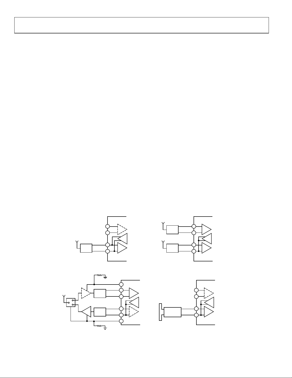
ADF7241
RF PORT CONFIGURATIONS/ANTENNA DIVERSITY
ADF7241 is equipped with two fully differential RF ports. Port 1
is capable of receiving, whereas Port 2 is capable of receiving or
transmitting. RF Port 1 comprises Pin RFIO1P and Pin RFIO1N,
and RF Port 2 comprises Pin RFIO2P and Pin RFIO2N. Only
one of the two RF ports can be active at any one time.
The availability of two RF ports facilitates the use of switched
antenna diversity and results in a simplified application circuit
if the ADF7241 is connected to an external LNA and/or PA.
Port selection for receive operation is configured through
Register rxfe_cfg, Field lna_sel (0x39B[4]).
Configuration A
Configuration A of Figure 49 is the default connection where a
single antenna is connected to RF Port 2. This selection is made
by setting Register rxfe_cfg, Field lna_sel = 1 (default setting).
Configuration B
Configuration B shows a dual-antenna configuration that is
suitable for switched antenna diversity. In this case, the link
margin can be maximized by comparing the RSSI level of the
signal received on each antenna and thus selecting the optimum
antenna. In addition, the SQI value in Register lrb, Field
sqi_readback can be used in the antenna selection decision.
Suitable algorithms for the selection of the optimum antenna
depend on the particulars of the underlying communication
system. Switching between two antennas is likely to cause a
short interruption of the received data stream. Therefore, it is
advisable to synchronize the antenna selection phase with the
preamble component of the packet. In a static communication
system, it is often sufficient to select the optimum antenna once.
Configuration C
Configuration C shows that connecting an external PA and/or
LNA is possible with a single external receive/transmit switch. The
PA transmits on RF Port 2. RF Port 1 is configured as the receive
input (Register rxfe_cfg, Field lna_sel = 0).
ADF7241 provides two signals, RXEN_GP6 and TXEN_GP5, to
automatically enable an external LNA and/or a PA. If Register
ext_ctrl, Field txen_en = 1, the ADF7241 outputs a logic high
level at the TXEN_GP5 pin while in TX state, and a logic low level
while in any other state. If Register ext_ctrl, Field rxen_en = 1, the
ADF7241 outputs a logic high level at the RXEN_GP6 pin while
in RX state and a logic low level while in any other state.
The RXEN_GP6 and TXEN_GP5 outputs have high impedance
in the sleep state. Therefore, appropriate pull-down resistors
must be provided to define the correct state of these signals
during power-down. See the PA R a mpi n g Control l er section for
further details on the use of an external PA, including details of
the integrated biasing block, which simplifies connection to PA
circuits based upon a single FET.
Configuration D
Configuration D is similar to Configuration A, except that a
dipole antenna is used. In this case, a balun is not required.
BALUN
BALUN
MATCH
RFIO1P
RFIO1N
RFIO2P
RFIO2N
B
RFIO1P
RFIO1N
RFIO2P
RFIO2N
D
4
LNA
5
PA
6
LNA
7
4
LNA
5
PA
6
LNA
7
09322-021
BALUN
LNA
PA
RFIO1P
RFIO1N
RFIO2P
RFIO2N
A
BALUN
BALUN
C
4
5
6
7
RXEN_GP6
RFIO1P
RFIO1N
RFIO2P
RFIO2N
TXEN_GP5
LNA
LNA
26
4
5
6
7
25
PA
LNA
LNA
PA
NETWORK
Figure 49. RF Interface Configuration Options (A: Single Antenna; B: Antenna Diversity; C: External LNA/PA; D: Dipole Antenna)
Rev. 0 | Page 42 of 72

ADF7241
AUXILLARY FUNCTIONS
TEMPERTURE SENSOR
To perform a temperature measurement, the MEAS state is
invoked using the RC_MEAS command. The result can be read
back from Register adc_rbk, Field adc_out (0x3AE[5:0]). Averaging multiple readings improves the accuracy of the result. The
temperature sensor has an operating range from −40°C to +85°C.
The die (ambient) temperature is calculated as follows:
t
= (4.72°C × Register adc_rbk, Field adc_out) + 65.58°C
die
+ correction value.
where correction value can be determined by performing a
readback at a single known temperature. Note also that averaging a number of ADC readbacks can improve the accuracy of the
temperature measurement.
BATTERY MONITOR
The battery monitor features very low power consumption and
can be used in any state other than the sleep state. The battery
monitor generates a batt_alert interrupt for the host MCU
when the battery voltage drops below the programmed
threshold voltage. The default threshold voltage is 1.7 V, and
can be increased in 62 mV steps to 3.6 V with Register bm_cfg,
Field battmon_voltage (0x3E6[4:0]).
WAKE-UP CONTROLLER (WUC)
Circuit Description
The ADF7241 features a 16-bit wake-up timer with a programmable prescaler. The 32.768 kHz RC oscillator or the 32.768 kHz
external crystal provides the clock source for the timer. This tick
rate clocks a 3-bit programmable prescaler whose output clocks
a preloadable 16-bit down counter. An overview of the timer
circuit is shown in Figure 50 lists the possible division rates for
the prescaler. This combination of programmable prescaler and
16-bit down counter gives a total WUC range of 30.52 μs to
36.4 hours.
Table 23. Prescaler Division Factors
Tick
timer_prescal (0x316[2:0]) 32.768 kHz Divider
000 1 30.52 μs
001 4 122.1 μs
010 8
011 16
100 128
101 1024
110 8,192
111 65,536 2000 ms
An interrupt generated when the wake-up timer has timed out
can be enabled in Register irq1_en0 or Register irq2_en0.
Period
244.1 μs
488.3 μs
3.91 ms
31.25 ms
250 ms
HARDWARE TIME R
32.768kHz
RC
OSCILLATOR
32.768kHz
XTAL
tmr_cfg1[6:3]
(ADDRESS 0x317)
32.768kHz T I CK RAT E
tmr_cfg0[2:0]
(ADDRESS 0x316)
PRESCALER
Figure 50. Hardware Wake-Up Timer Diagram
tmr_rld0[15:8], tmr_rld1[7:0]
(ADDRESS 0x318, 0x319)
16-BIT DOWN
COUNTER
WAKE UP
irq_src0[2]
(ADDRESS 0x3CB)
09322-042
Rev. 0 | Page 43 of 72

ADF7241
WUC Configuration and Operation
The wake-up timer can be configured as follows:
• The clock signal for the timer is taken from the external
32.768 kHz crystal or the internal RC oscillator. This is
selectable via Register tmr_cfg1, Field sleep_config
(0x317[6:3]).
• A 3-bit prescaler, which is programmable via Register
tmr_cfg0, Field timer_prescal (0x316[2:0]) determines the
tick period.
This is followed by a preloadable 16-bit down counter. After the
clock is selected, the reload value for the down counter
(tmr_rld0 and tmr_rld1) and the prescaler values (Register
tmr_cfg0, Field timer_prescal) can be programmed. When the
clock has been enabled, the counter starts to count down at the
tick rate starting from the reload value. If wake-up interrupts
are enabled, the timer unit generates an interrupt when the
timer value reaches 0x0000. When armed, the wake-up
interrupt triggers a wake-up from sleep.
The reliable generation of wake-up interrupts requires the
WUC timeout flag to be reset immediately after the reload value
has been programmed. To do this, first write 1 and then write 0
to Register tmr_ctrl, Field wake_timer_flag_reset. To enable
automatic wake-up from the sleep state, arm the timer unit for
wake-up operation by writing 1 to Register tmr_cfg1, Field
wake_on_timeout. After writing this sequence to the ADF7241,
a sleep command can be issued.
Calibrating the RC oscillator
The RC oscillator is not automatically calibrated. If it is desired
to use the RC oscillator as the clock source for the WUC, the
host MCU should initiate a calibration. This can be performed
at any time in advance of entering the sleep state. To perform a
calibration, the host MCU should
• Set Register tmr_ctrl, Field wuc_rc_osc_cal = 0
• Set Register tmr_ctrl, Field wuc_rc_osc_cal = 1
The calibration time is typically 1 ms. When the calibration is
complete Register wuc_32khzosc_status, Field rc_osc_cal_ready
is high. Following calibration, the host MCU can transition to
the SLEEP_BBRAM_RCO sleep state, by following the full
procedure given in the WUC Configuration and Operation
section.
TRANSMIT TEST MODES
The ADF7241 has various transmit test modes that can be used
in SPORT mode. These test modes can be enabled by writing to
Register tx_test (Location 0x3F0), as described in Ta b le 2 4. A
continuous packet transmission mode is also available in packet
mode. This mode can be enabled using the following procedure:
1. An IEEE 80.215.4-2006 packet with random payload
should be written to TX_BUFFER as described in the
Tr an sm it t er section. It is recommended to use a packet
with the maximum length of 127 bytes.
2. Set Register buffercfg, Field trx_mac_delay = 1.
3. Set Register buffercfg, Field tx_buffer_mode = 3.
4. Set Register pkt_cfg, Field skip_synth_settle = 1.
5. Issue Command RC_TX. The transmitter continuously
transmits the packet stored in TX_BUFFER.
6. If Command RC_PHY_RDY is issued at any point after
this step, all the preceding configuration registers must be
rewritten to the device before reissuing Command RC_TX.
Note that the transmitter momentarily transmits an RF carrier
between packets due to a finite delay from when the packet
handler finishes transmitting a packet in TX_BUFFER and
going back to transmit the start of TX_BUFFER again.
Table 24. 0x3F0: tx_test
Bit Name R/W Reset Value Description
[7:2] Reserved R/W 2 Reserved, set to default.
1 carrier_only R/W 0 Transmits unmodulated tone at the programmed frequency fCH.
0 Reserved R/W 0 Reserved, set to default.
Rev. 0 | Page 44 of 72

ADF7241
V
SERIAL PERIPHERAL INTERFACE (SPI)
CS
GENERAL CHARACTERISTICS
The ADF7241 is equipped with a 4-wire SPI interface, using the
CS
SCLK, MISO, MOSI, and
a slave to the host MCU. shows an example connec-
pins. The ADF7241 always acts as
Figure 51
tion diagram between the host MCU and the ADF7241. The
diagram also shows the direction of the signal flow for each pin.
The SPI interface is active and the MISO output enabled only
while the
CS
input is low. The interface uses a word length of
eight bits, which is compatible with the SPI hardware of most
microprocessors. The data transfer through the SPI interface
occurs with the most significant bit of address and data first.
Refer to for the SPI interface timing diagram. The
Figure 3
MOSI input is sampled at the rising edge of SCLK. As commands or data are shifted in from the MOSI input at the SCLK
rising edge, the status word or data is shifted out at the MISO
pin synchronous with the SCLK clock falling edge. If
CS
is
brought low, the most significant bit of the status word appears
on the MISO output without the need for a rising clock edge on
the SCLK input.
BAT
ADF7241
IRQ1_GP4
IRQ2_TRFS_GP2
DR_GP0
DT_GP1
TRCLK_CKO_GP3
CS
SCLK
MOSI
MISO
Figure 51. SPI Interface Connection
PF1
SCLK
MOSI
MISO
GPI
RFS
DR
DT
RSCLK
TSCLK
ADSP-21xx
OR
BLACKFIN
DSP
09322-031
COMMAND ACCESS
The ADF7241 is controlled through commands. Command
words are single-byte instructions that control the state
transitions of the radio controller and access to the registers and
packet RAM. The complete list of valid commands is given in
Tabl e 2 5 . Commands with the RC prefix are handled by the
radio controller, whereas memory access commands, which
have the SPI prefix are handled by an independent controller.
Thus, SPI commands can be issued independent of the state of
the radio controller.
A command is initiated by bringing
command word over the SPI as shown in . Figure 52
CS
low and shifting in the
All commands are executed after
next positive edge of the SCLK input. The latter condition
occurs in the case of a memory access command. In this case,
the command is executed on the positive SCLK clock edge
corresponding to the most significant bit of the first parameter
word. The
CS
input must be brought high again after a
command has been shifted into the ADF7241 to enable the
recognition of successive command words. This is because a
single command can be issued only during a
(with the exception of a double NOP command).
CS
MOSI
MISO
Figure 52. Command Write
The execution of certain commands by the radio controller may
take several instruction cycles, during which the radio controller unit is busy. Prior to issuing a radio controller command, it
is, therefore, necessary to read the status word to determine if
the ADF7241 is ready to accept a new radio controller command.
This is best accomplished by shifting in SPI_NOP commands,
which cause status words to be shifted out. The RC_READY
variable is used to indicate when the radio controller is ready to
accept a new RC command, whereas the SPI_READY variable
indicates when the memory can be accessed. To take the burden
of repeatedly polling the status word off the host MCU for
complex commands such as RC_RX, RX_TX, and RC_PHY_RDY,
the IRQ handler can be configured to generate an RC_READY
interrupt. See the Interrupt Controller section for details.
Otherwise, the user can program timeout periods according to
the command execution times provided under the state transition timing given in Tabl e 10 .
STATUS WORD
The status word of the ADF7241 is automatically returned over
the MISO each time a byte is transferred over the MOSI. The
meaning of the various status word bit fields is illustrated in
Tabl e 2 6 . The RC_STATUS field reflects the current state of the
radio controller. By definition, RC_STATUS reflects the state of
a completed state transition. During the state transition,
RC_STATUS maintains the value of the state from which the
state transition was invoked.
goes high again or at the
RC OR SPI
COMMAND
STATUS
CS
low period
09322-038
Rev. 0 | Page 45 of 72

ADF7241
Table 25. Command List
Command Code Description
SPI_NOP 0xFF No operation. Use for dummy writes.
SPI_PKT_WR 0x10
SPI_PKT_RD 0x30
SPI_MEM_WR 0x18 + memory address[10:8] Write data to MCR or packet RAM sequentially.
SPI_MEM_RD 0x38 + memory address[10:8] Read data from MCR or packet RAM sequentially.
SPI_MEMR_WR 0x08 + memory address[10:8] Write data to MCR or packet RAM as a random block.
SPI_MEMR_RD 0x28 + memory address[10:8] Read data from MCR or packet RAM as a random block.
SPI_PRAM_WR 0x1E Write data to the program RAM.
RC_SLEEP 0xB1 Invoke transition of the radio controller into the sleep state
RC_IDLE 0xB2 Invoke transition of the radio controller into the idle state
RC_PHY_RDY 0xB3 Invoke transition of the radio controller into the PHY_RDY state
RC_RX 0xB4 Invoke transition of the radio controller into the RX state
RC_TX 0xB5 Invoke transition of the radio controller into the TX state
RC_MEAS 0xB6 Invoke transition of the radio controller into the MEAS state
RC_CCA 0xB7 Invoke clear channel assessment
RC_PC_RESET 0xC7
RC_RESET 0xC8 Resets the ADF7241 and puts it in the sleep state
Write data to the packet RAM starting from the transmit packet base address pointer,
Register txpb, Field tx_pkt_base (0x314[7:0]).
Read data from the packet RAM starting from the receive packet base address pointer,
Register rxpb, Field rx_pkt_base (0x315[7:0]).
Program counter reset. This should only be used after a firmware download to the
program RAM
Table 26. SPI Status Word
Bit Name Description
7 SPI_READY 0: SPI is not ready for access.
1: SPI is ready for access.
6 IRQ_STATUS 0: no pending interrupt condition.
1: pending interrupt condition. (IRQ_STATUS = 1 when either the IRQ1_GP4 or
IRQ2_TRFS_GP2 pin is high)
5 RC_READY 0: radio controller is not ready to accept RC_xx command strobe.
1: radio controller is ready to accept new RC_xx command strobe.
4 CCA_RESULT 0: channel busy.
1: channel idle.
Valid when Register irq_src1, Bit cca_complete (0x3CC[0]) is asserted.
[3:0] RC_STATUS Radio controller status:
0: reserved.
1: idle.
2: MEAS.
3: PHY_RDY.
4: RX.
5: TX.
6 to 15: reserved.
Rev. 0 | Page 46 of 72

ADF7241
MEMORY MAP
The various memory locations used by the ADF7241 are shown
in Figure 53. The radio control and packet management of the
part are realized through the use of an 8-bit, custom processor,
and an embedded ROM. The processor executes instructions
stored in the embedded program ROM. There is also a local
RAM, subdivided into three sections, that is used as a data
packet buffer, both for transmitted and received data (packet
RAM), and for storing the radio and packet management
configuration (BBRAM and MCR). The RAM addresses of
these variables are 11 bits in length.
BBRAM
The 64-byte battery back-up, or BBRAM, is used to maintain
settings needed at wake-up from sleep state by the wake-up
controller.
MODEM CONFIGURATION RAM (MCR)
The 256-byte modem configuration RAM, or MCR, contains
the various registers used for direct control or observation of
the physical layer radio blocks of the ADF7241. Contents of the
MCR are not retained in the sleep state.
PROGRAM ROM
The program ROM consists of 4 kB of nonvolatile memory. It
contains the firmware code for radio control, packet management, and smart wake mode.
PROGRAM RAM
The program RAM consists of 2 kB of volatile memory. This
memory space is used for various software modules, such as
address filtering and CSMA/CA, which are available from
Analog Devices. The software modules are downloaded to the
program RAM memory space over the SPI by the host
microprocessor. See the Program RAM Write subsection of the
Memory Access section for details on how to write to the
program RAM.
PACKET RAM
The packet RAM consists of 256 bytes of memory space from
Address 0x000 to Address 0x0FF, as shown in Figure 53. This
memory is allocated for storage of data from valid received
packets and packet data to be transmitted. The packet manager
stores received payload data at the memory location indicated
by the value of Register rxpb, Field rx_pkt_base, the receive
address pointer. The value of Register txpb, Field tx_pkt_base,
the transmit address pointer, determines the start address of
data to be transmitted by the packet manager. This memory can
be arbitrarily assigned to store single or multiple transmit or
receive packets, both with and without overlap as shown in
Figure 54. The rx_pkt_base value should be chosen to ensure
that there is enough allocated packet RAM space for the
maximum receiver payload length.
11-BIT
ADDRESSES
0x3FF
MCR
256 BYTES
0x300
NOT USED
0x13F
BBRAM
64 BYTES
0x100
0x0FF
PACKET
RAM
256 BYTES
0x000
09322-070
PACKET
MANAGER
CLOCK
REGISTER prampg, FIELD pram_page[3:0]
CS
MISO
MOSI
SCLK
SPI
PACKET
MANAGER
8-BIT
PROCESSOR
ADDRESS
SPI/PH
MEMORY
ARBITRATION
ADDRESS/
DATA
MUX
[7:0]
PROGRAM
RAM
2kB
PROGRAM
ROM
4kB
INSTRUCTION/DATA
[7:0]
ADDRESS[10:0]
DATA[7:0]
Figure 53. ADF7241 Memory Map
Rev. 0 | Page 47 of 72

ADF7241
T
tx_pkt_base
rx_pkt_base
TRANSMIT
AND RECEIVE
PACKET
TRANSMIT
PAYLOAD
RECEIVE
PAYLOAD
0x000
0x0FF
tx_pkt_base
rx_pkt_base
256-BYTE TRANSMI
OR RECEIVE
PACKET
TRANSMIT OR
RECEIVE
PAYLOAD
0x000
0x0FF
tx_pkt_base
(PACKET 1)
tx_pkt_base
(PACKET 2)
rx_pkt_base
(PACKET 1)
rx_pkt_base
(PACKET 2)
MULTIP LE TRANSMIT
AND RECEIVE
PACKETS
TRANSMIT
PAYLOAD
TRANSMIT
PAYLOAD 2
RECEIVE
PAYLOAD
RECEIVE
PAYLOAD 2
0x000
0x0FF
09322-071
Figure 54. Example Packet RAM Configurations Using the Transmit Packet and Receive Packet Address Pointers
Rev. 0 | Page 48 of 72

ADF7241
MEMORY ACCESS
Memory locations are accessed by invoking the relevant SPI
command. An 11-bit address is used to identify registers or
locations in the memory space. The most significant three bits
of the address are incorporated into the command by appending them as the LSBs of the command word. Figure 55
illustrates the command, address, and data partitioning. The
various SPI memory access commands are different depending
on the memory location being accessed. This is described in
Tabl e 2 7 .
CS
An SPI command should be issued only if the SPI_READY bit
of the status word is high.
In addition, an SPI command should not be issued while the
radio controller is initializing. SPI commands can be issued in
any radio controller state including during state transition.
SPI_MEM_WR MEMORY A DDRE SS
MOSI
5 BITS M E M O RY ADDR ES S
Figure 55. SPI Memory Access Command/Address Format
BITS[10:0]
Table 27. Summary of SPI Memory Access Commands
SPI Command Command Value Description
SPI_PKT_WR = 0x10
Write telegram to the packet RAM starting from the transmit packet base address pointer,
Register txpb, Field tx_pkt_base (0x314[7:0]).
SPI_PKT_RD = 0x30
Read telegram from the packet RAM starting from receive packet base address pointer,
Register rxpb, Field rx_pkt_base (0x315[7:0]).
SPI_MEM_WR = 0x18 (packet RAM)
= 0x19 (BBRAM)
= 0x1B (MCR)
SPI_MEM_RD = 0x38 (packet RAM)
= 0x39 (BBRAM)
= 0x3B (MCR)
Write data to BBRAM, MCR, or packet RAM sequentially. An 11-bit address is used to identify
memory locations. The most significant three bits of the address are incorporated into the
command (xxxb). This command is followed by the remaining eight bits of the address.
Read data from BBRAM, MCR, or packet RAM sequentially. An 11-bit address is used to identify
memory locations. The most significant three bits of the address are incorporated into the
command (xxxb). This command is followed by the remaining eight bits of the address, which
is subsequently followed by the appropriate number of SPI_NOP commands.
SPI_MEMR_WR = 0x08 (packet RAM)
Write data to BBRAM/MCR or packet RAM at random.
= 0x09 (BBRAM)
= 0x0B (MCR)
SPI_MEMR_RD = 0x28 (packet RAM)
Read data from BBRAM/MCR or packet RAM at random.
= 0x29 (BBRAM)
= 0x2B (MCR)
SPI_PRAM_WR =0x1E (program RAM)
SPI_PRAM_RD = 0x3E (program RAM)
SPI_NOP = 0xFF
Write data to program RAM.
Read data from program RAM
No operation. Use for dummy writes when polling the status word and used as dummy data on
the MOSI line when performing a memory read.
BITS[7: 0] DATA BYTE
DATA
n × 8 BITS
09322-072
Rev. 0 | Page 49 of 72

ADF7241
WRITING TO THE ADF7241
Block Write
Packet RAM memory locations can be written to in block
format using the SPI_PKT_WR. The SPI_PKT_WR command
is 0x10. This command provides pointer-based write access to
the packet RAM. The address of the location written to is calculated from the base address in Register txpb, Field tx_pkt_base
(0x314[7:0]), plus an index. The index is zero for the first data
word following the command word and is auto-incremented
for each consecutive data word written. The first data word following an SPI_PKT_WR command is, thus, stored in the location
with Address txpb, Field tx_pkt_base (0x314[7:0]), the second
in packet RAM location with Address txpb, Field tx_pkt_base + 1,
and so on. This feature makes this command efficient for bulk
writes of data that recurrently begin at the same address. Figure 56
shows the access sequence for Command SPI_PKT_WR.
The MCR, BBRAM, and packet RAM memory locations can be
written to in block format using the SPI_MEM_WR command.
The SPI_MEM_WR command code is 00011xxxb, where xxxb
represent Bits[10:8] of the first 11-bit address. If more than one
data byte is written, the write address is automatically incremented for every byte sent until
the memory access command. See for more details.
The maximum block write for the MCR, packet RAM, and
BBRAM memories are 256 bytes, 256 bytes, and 64 bytes,
respectively. These maximum block-write lengths should not be
exceeded.
Example
Write 0x00 to the rc_cfg register (Location 0x13E).
• The first five bits of the SPI_MEM_WR command are
00011.
• The 11-bit address of rc_cfg is 00100111110.
• The first byte sent is 00011001 or 0x19.
• The second byte sent is 00111110 or 0x3E.
• The third byte sent is 0x00.
Thus, 0x193F00 is written to the part.
Random Address Write
MCR, BBRAM, and packet RAM memory locations can be
written to in random address format using the SPI_MEMR_WR
command. The SPI_MEMR_WR command code is 00001xxxb,
where xxxb represent Bits[10:8] of the 11-bit address. The lower
eight bits of the address should follow this command and then
the data byte to be written to the address. The lower eight bits of
the next address are entered followed by the data for that
address until all required addresses within that block are
written, as shown in Figure 58. Note that the SPI_MEMR_WR
command facilitates the modification of individual elements of
a packet in RX_BUFFER and TX_BUFFER without the need to
download and upload an entire packet.
The address location of a particular byte in RX_BUFFER and
TX_BUFFER in the packet RAM is determined by adding the
CS
is set high, which terminates
Figure 57
Rev. 0 | Page 50 of 72
relative location of a byte to Address Pointer rx_pkt_base
(Register rxpb; 0x315[7:0]) or Address Pointer tx_pkt_base
(Register txpb; 0x314[7:0]), respectively.
Program RAM Write
The program RAM can only be written to using the memory
block write, as illustrated in Figure 59. The SPI_PRAM_WR
command is 0x1E. The program RAM is organized in eight
pages with a length of 256 bytes each. The code module must be
stored in the program RAM starting from Address 0x0000, or
Address 0x00 in Page 0. The current program RAM page is
selected with Register prampg, Field pram_page (0x313[3:0]).
Prior to uploading the program RAM, the radio controller code
module must be divided into blocks of 256 bytes commensurate
with the size of the program RAM pages. Each 256-byte block is
uploaded into the currently selected program RAM page using
the SPI_PRAM_WR command. Figure 59 illustrates the
sequence required for uploading a code block of 256 bytes to a
PRAM page. The SPI_PRAM_WR command code is followed
by Address Byte 0x00 to align the code block with the base
address of the program RAM page. Figure 60 shows the overall
upload sequence. With the exception of the last page written to
the program RAM, all pages must be filled with 256 bytes of
module code.
READING FROM THE ADF7241
Block Read
Command SPI_PKT_RD provides pointer-based read access
from the packet RAM. The SPI_PKT_RD command is 0x30.
The address of the location to be read is calculated from the base
address in Register rxpb, Field rx_pkt_base, plus an index. The
index is zero for the first readback word. It is auto-incremented
for each consecutive SPI_NOP command. The first data byte
following a SPI_PKT_RD command is invalid and should be
ignored. Figure 61 shows the access sequence for Command
SPI_PKT_RD.
The SPI_MEM_RD command can be used to perform a block
read of MCR, BBRAM, and packet RAM memory locations.
The SPI_MEM_RD command code is 00111xxxb, where xxxb
represent Bits[10:8] of the first 11-bit address. This command is
followed by the remaining eight bits of the address to be read
and then two SPI_NOP commands (dummy byte). The first
byte available after writing the address should be ignored, with
the second byte constituting valid data. If more than one data
byte is to be read, the read address is automatically incremented
for subsequent SPI_NOP commands sent. See Figure 62 for
more details.
Random Address Read
MCR, BBRAM, and Packet RAM memory locations can be read
from in a nonsequential manner using the SPI_MEMR_RD
command. The SPI_MEMR_RD command code is 00101xxxb,
where xxxb represent Bits[10:8] of the 11-bit address. This
command is followed by the remaining eight bits of the address
to be written and then two SPI_NOP commands (dummy byte).
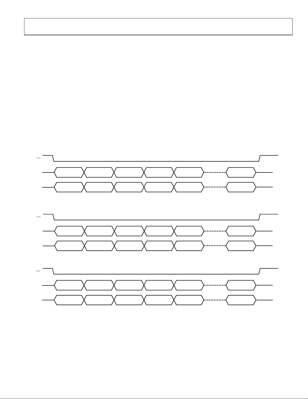
ADF7241
The data byte from memory is available on the second SPI_NOP
command. For each subsequent read, an 8-bit address should be
followed by two SPI_NOP commands as shown in Figure 63.
Example
Read the value stored in the rc_cfg register.
• The first five bits of the SPI_MEM_RD command are 00111.
• The 11-bit address of rc_cfg register is 00100111111.
• The first byte sent is 00111001, or 0x39.
• The second byte sent is 00111110, or 0x3E.
• The third byte sent is 0xFF (SPI_NOP).
• The fourth byte sent is 0xFF.
CS
Thus, 0x393EFFFF is written to the part.
The value shifted out on the MISO line while the fourth byte is
sent is the value stored in the rc_cfg register.
This allows individual elements of a packet in RX_BUFFER and
TX_BUFFER to be read without the need to download the
entire packet.
Program RAM Read
The SPI_PRAM_RD command is used to read from the
program RAM. This may be performed to verify that a
firmware module has been correctly written to the program
RAM. Like the SPI_PRAM_WR command, the host MCU must
select the program RAM page to read via Register prampg, Field
pram_page. Following this, the host MCU may use the
SPI_PRAM_RD command to block read the selected program
RAM page. The structure of this command is identical to the
SPI_MEM_RD command.
[MAX N = (256 – tx_p kt _base)]
MOSI
MISO
SPI_PKT_WR
STATUS STATUS STATUS STATUS STATUS STATUS
DATA FOR ADDRESS
[tx_pkt_base]
DATAFOR ADDRESS
[tx_pkt_base + 1]
DATA FOR ADDRESS
[tx_pkt_base + 2]
DATAFOR ADDRESS
[tx_pkt_base + 3]
DATAFOR ADDRESS
[tx_pkt_base + N]
09322-033
Figure 56. Packet RAM Write
(tx_pkt_base is the address base pointer value for TX, which is programmed in Register txbp, Bit tx_pkt_base.)
CS
MOSI
MISO
SPI_MEM_WR
STATUS STATUS STATUS STATUS STATUS STATUS
ADDRESS
DATA FOR
[ADDRESS]
DATA FOR
[ADDRESS + 1]
DATA FOR
[ADDRESS + 2]
Figure 57. Memory (Register or Packet RAM) Block Write
[MAX N = (256 – INITIAL ADDRESS)]
DATA FOR
[ADDRESS + N]
09322-032
CS
MOSI
MISO
SPI_MEMR_WR
STATUS STATUS STATUS STATUS STATUS STATUS
ADDRESS 1 DATA 1 ADDRESS 2 DATA 2 DATA N
09322-036
Figure 58. Memory (Register or Packet RAM) Random Address Write
Rev. 0 | Page 51 of 72

ADF7241
CS
MOSI
MISO
SPI_MEM_WR
+0x03
0x13
PAGE NUMBER
n
STATUSSTATUSSTATUS
SPI_PRAM_WR
UPLOAD 256 BY TES OF C ODE TO P RA M P A GE NUMBER nSET PRAM P AGE NUMBER n
0x00
CODE[0x00]
STATUS
CODE[0xFF]
STATUSSTATUSSTATUS
09322-073
Figure 59. Upload Sequence for a Program RAM Page
SET PRAM PAGE 0 SET PRAM PAGE 1 SET PRAM PAGE 2
DOWNLOAD 256 BY TES BLOCK 0
TO PRAM PAGE 0
Figure 60. Download Sequence for Code Module
DOWNLOAD 256 BYTES BLOCK 0
TO PRAM PAGE 1
9322-074
CS
MOSI
MISO
SPI_PKT_RD SPI_NOP SPI_NOP SPI_NOP SPI_NOP SPI_NOP
STATUS STATUS
DATAFROM
ADDRESS
rx_pkt_base
DATAFROM
ADDRESS
rx_pkt_base + 1
DATA FROM
ADDRESS
rx_pkt_base + 2
Figure 61. Packet RAM Read
(rx_pkt_base is the address base pointer value for RX, which is programmed in Register rxbp, Bit rx_pkt_base.)
MAX N = (256 – tx_pkt_base)
DATA FROM
ADDRESS
rx_pkt_base + N
09322-035
CS
[MAX N = (256 – INITIALADDRESS)]
CS
MOSI
MISO
MOSI
MISO
SPI_MEM_RD
STA TUS STATUS STATUS
SPI_MEM_RD
STATUS STATUS STATUS
ADDRESS 1
ADDRESS SPI_NOP SPI_NOP SPI_NOP SPI_NOP
ADDRESS 2
DATA FROM
ADDRESS
DATA FROM
ADDRESS + 1
Figure 62. Memory (Register or Packet RAM) Block Read
ADDRESS 3
DATA FROM
ADDRESS 1
ADDRESS 4
DATA FROM
ADDRESS 2
ADDRESS N
DATA FROM
ADDRESS N – 2
Figure 63. Memory (Register or Packet RAM) Random Address Read
DATA FROM
ADDRESS + N
SPI_NOP
DATA FROM
ADDRESS N – 1
SPI_NOP
DATA FROM
ADDRESS N
09322-034
09322-037
Rev. 0 | Page 52 of 72

ADF7241
DOWNLOADABLE FIRMWARE MODULES
The program RAM of the ADF7241 can be used to store
firmware modules for the on-chip processor that provide extra
functionality. The executable code for these firmware modules
and details on their functionality are available from Analog
Devices. See the Writing to the ADF7241 section for details on
how to download these firmware modules to program RAM.
Rev. 0 | Page 53 of 72

ADF7241
INTERRUPT CONTROLLER
CONFIGURATION
The ADF7241 is equipped with an interrupt controller that is
capable of handling up to 16 independent interrupt events. The
interrupt events can be triggered either by hardware circuits or
the packet manager and are captured in Register irq_src0
(0x3CB) and Register irq_src1(0x3CC).
The interrupt signals are available on two interrupt pins: IRQ1_
GP4 and IRQ2_TRFS_GP2. Each of the 16 interrupt sources
can be individually enabled or disabled. The irq1_en0 (0x3C7)
and irq1_en1 (0x3C8) registers control the functionality of the
IRQ1_GP4 interrupt pin. The irq2_en0 (0x3C9) and irq2_en1
(0x3CA) registers control the functionality of the IRQ2_TRFS_
GP2 interrupt pin. Refer to Ta ble 2 8 and Tab l e 2 9 for details on
which bits in the relevant interrupt source and interrupt enable
registers correspond to the different interrupts.
The IRQ_STATUS bit of the SPI status word, is asserted if an
interrupt is present on either IRQ1 or IRQ2. This is useful for
host MCUs that may not have interrupt pins available.
The irq_src1 and irq_src0 registers can be read back to establish
the source of an interrupt. An interrupt is cleared by writing 1
to the corresponding bit location in the appropriate interrupt
source register (irq_src1 or irq_src0). If 0 is written to a bit
location in the interrupt source registers, its state remains
unchanged. This scheme allows interrupts to be cleared
individually and facilitates hierarchical interrupt processing.
The availability of two interrupt outputs permits a flexible
allocation of interrupt source to two different MCU hardware
REGISTER irq_src1 REGISTER irq_src0
resources. For instance, an rx_sfd interrupt can be associated
with a timer-capture unit of the MCU, while all other interrupts
are handled by a normal interrupt handling routine. When
operating in SPORT mode, Pin IRQ2_TRFS_GP2 acts as a
frame synchronization signal and is disconnected from the
interrupt controller.
When in the sleep state, the IRQ1_GP4 and IRQ2_TRFS_GP2
pins have high impedance.
When not in the sleep state, Pin IRQ1_GP4 and Pin IRQ2_
TRFS_GP2 are configured as push-pull outputs, using positive
logic polarity.
Following a power-on reset or wake-up from sleep, Register
irq1_en0, Field powerup and Register irq2_en0, Field powerup
are set, while all other bits in the irq1_en0, irq1_en1, irq2_en0,
and irq2_en1 registers are reset. Therefore, a power-up interrupt
signal is asserted on the IRQ1_GP4 and IRQ2_TRFS_GP2 pins
after a power-on-reset event or wake-up from the sleep state.
Provided the wake-up from sleep event is caused by the wakeup timer, the power-up interrupt signal can be used to power
up the host MCU.
After the ADF7241 is powered up, the rc_ready, wake-up, and
power-on reset interrupts are also asserted in the irq_src0
register. However, these interrupts are not propagated to the
IRQ1_GP4 and IRQ2_TRFS_GP2 pins because the corresponding mask bits are reset. The irq_src0 and irq_src1 registers
should be cleared during the initialization phase.
INTERRUPT
SOURCES
(16 INTERR UPT SOURCE S
AVAILABLE)
INTERRUPT
MASKS
(2 × 16 INDEP ENDENT
INTERRUPT MASKS)
INTERRUPT OUTPUTS
(2 INTERRU P T PINS AND
INTERRUPT PENDING BIT
AVAILABL E ON THE
STATUS_WORD)
tx_sfd
RESERVED
RESERVED
RESERVED
tx_pkt_sent
15 14 13 12 11 10 9 8
REGISTER irq1_en1 REGISTER irq1_en0
Figure 64. Interrupt Controller
rx_sfd
rx_pkt_rcvd
Status_word[6]IRQ1_GP4 IRQ2_TRFS_GP2
RESERVED
cca_complete
76543210
REGISTER irq2_en1 REGISTER irq2_en0
RESERVED
por
wakeup
rc_ready
batt_alert
powerup
RESERVED
09322-094
Rev. 0 | Page 54 of 72

ADF7241
Table 28. Bit Locations in the Interrupt Source Register
irq_src1, with Corresponding Interrupt Enables in irq1_en1,
irq2_en1
Bit Name Notes
7 Reserved Don’t care; set mask to 0.
6 Reserved Don’t care; set mask to 0.
5 Reserved Don’t care; set mask to 0.
4 tx_pkt_sent TX packet transmission complete.
3 rx_pkt_rcvd Packet received in RX_BUFFER.
2 tx_sfd SFD has been transmitted.
1 rx_sfd SFD has been detected.
0 cca_complete CCA_RESULT in status word is valid.
Table 29. Bit Locations in the Interrupt Source Register
irq_src0, with Corresponding Interrupt Enables in irq1_en0,
irq2_en0
Bit Name Notes
7 Reserved Don’t care; set mask to 0.
6 Reserved Don’t care; set mask to 0.
5 batt_alert
4 por Power-on reset event.
3 rc_ready
2 wakeup Timer has timed out.
1 powerup Chip is ready for access.
0 Reserved Don’t care; set mask to 0.
Battery voltage has dropped below
programmed threshold value.
Radio controller ready to accept new
command.
DESCRIPTION OF INTERRUPT SOURCES
tx_pkt_sent
This interrupt is asserted when in IEEE 802.15.4-2006 packet
mode and the transmission of a packet in TX_BUFFER is
complete.
rx_pkt_rcvd
This interrupt is asserted when in IEEE 802.15.4-2006 packet
mode and a packet with a valid FCS has been received and is
available in RX_BUFFER.
tx_sfd
This interrupt is asserted if the SFD is transmitted when in
IEEE 802.15.4-2006 packet mode.
rx_sfd
This interrupt is asserted if a SFD is detected while in the RX
state in either IEEE 802.15.4 mode.
cca_complete
The interrupt is asserted at the end of a CCA measurement
following a RC_RX or RC_CCA command. The interrupt
indicates that the CCA_RESULT flag in the status word is valid.
batt_alert
The interrupt is asserted if the battery monitor signals a battery
alarm. This occurs when the battery voltage drops below the
programmed threshold value. The battery monitor must be
enabled and configured. See the Battery Monitor section for
further details.
rc_ready
The interrupt is asserted if the radio controller is ready to accept
a new command. This condition is equivalent to the rising edge
of the RC_READY flag in the status word.
wakeup
The interrupt is asserted if the WUC timer has decremented to
zero. Prior to enabling this interrupt, the WUC timer unit must
be configured with the tmr_cfg0, tmr_cfg1, tmr_rld0, and
tmr_rld1 registers. A wake-up interrupt can be asserted while
the ADF7241 is active or has woken up from the sleep state
through a timeout event. See the Wak e -Up C ont rol le r (W U C)
section or further details.
powerup
The interrupt is asserted if the ADF7241 is ready for SPI access
following a wake-up from the sleep state. This condition reflects
a rising edge of the flag SPI_READY in the status word. If the
ADF7241 has been woken up from the sleep state using the
CS
input, this interrupt is useful to detect that the ADF7241 has
powered up without the need to poll the MISO output. Register
irq1_mask, Field powerup and Register irq2_mask, Field
powerup are automatically set on exit from the sleep state.
Therefore, this interrupt is generated when a transition from
sleep is triggered by
CS
being pulled low or by a timeout event.
Rev. 0 | Page 55 of 72

ADF7241
APPLICATIONS CIRCUITS
C28C41C40C39C14C15
GND
UNBAL
GND
BALP
BALM
C32
32kHz
VBAT
2526272829303132
CS
MOSI
SCLK
MISO
DT_GP1
R10
24
23
22
21
20
19
18
17
C18
C21
C22
10
C25
C26
12
R12
C17
C27
C16
1
CREGRF1
2
RBIAS
3
CREGRF2
4
RFIO1P
5
RFIO1N
6
RFIO2P
7
RFIO2N
8
CREGRF3
VDD_BAT
PAVSUP_ATB3
PABIAOP_ATB4
XOSC32KN_ATB2
XOSC32KP_GP7_ATB1
ADF7241
CREGVCO
PADDLE
VCOGUARD
CREGSYNTH
XOSC26P
XOSC26N
26MHz
TXEN_GP5
RXEN_GP6
CREGDIG1
TRCLK_CKO_GP3
IRQ2_TRFS_GP2
DGUARD
CREGDIG2
DR_GP0
161514131211109
IRQ1_GP4
SENSOR
SCS
MOSI
SCLK
MISO
MICRO-
CONTROLLER
GPIO0
GPIO1
MOSI
SCLK
MISO
IRQ1IN
IRQ2IN
Figure 65. Typical ADF7241 Application Circuit Using Antenna Diversity
C37C36C35C34C32C30C29
09322-044
Rev. 0 | Page 56 of 72

ADF7241
C28C41C40C39C14C15
32kHz
VBAT
2526272829303132
CS
MOSI
SCLK
MISO
C37C36C35C34C32C30C29
R10
24
23
22
21
20
19
18
17
BFxxx
GPIO1
MOSI
SCLK SPI
MISO
IRQ1IN
SPORT
RCLK
TCLK
DSP
RFS
DT
DR
09322-045
C10
C4
L3
C6
L2
L1
L4
C8
L6
C11
L5
C18
C5
C7
C9
R12
C17
C27
C16
1
CREGRF1
2
RBIAS
3
CREGRF2
4
RFIO1P
5
RFIO1N
6
RFIO2P
7
RFIO2N
8
CREGRF3
VDD_BAT
PAVSUP_ATB3
PABIAOP_ATB4
XOSC32KN_ATB2
XOSC32KP_GP7_ATB1
ADF7241
CREGVCO
PADDLE
VCOGUARD
CREGSYNTH
XOSC26P
XOSC26N
26MHz
TXEN_GP5
RXEN_GP6
CREGDIG1
TRCLK_CKO_GP3
IRQ2_TRFS_GP2
DGUARD
CREGDIG2
DR_GP0
161514131211109
IRQ1_GP4
DT_GP1
Figure 66. Typical ADF7241 Application Circuit with DSP Using Antenna Diversity
Rev. 0 | Page 57 of 72

ADF7241
C28C41
R14
R15
VBAT
C39C14C15
32kHz
C40
2526272829303132
LNA
ENABLE
ENABLE
PA
GND
UNBAL
GND
GND
UNBAL
GND
BALP
BALM
BALP
BALM
C18
C21
C22
10
C25
C26
12
R12
C17
C27
C16
1
CREGRF1
2
RBIAS
3
CREGRF2
4
RFIO1P
5
RFIO1N
6
RFIO2P
7
RFIO2N
8
CREGRF3
VDD_BAT
PAVSUP_ATB3
PABIAOP_ATB4
XOSC32KN_ATB2
XOSC32KP_GP7_ATB1
ADF7241
CREGVCO
PADDL E
VCOGUARD
CREGSYNTH
XOSC26P
XOSC26N
26MHz
Figure 67. Typical ADF7241 Application Circuit with External LNA and External PA
TXEN_GP5
CREGDIG1
RXEN_GP6
TRCLK_CKO_GP3
IRQ2_TRFS_GP2
DGUARD
CREGDIG2
DR_GP0
161514131211109
MOSI
SCLK
MISO
IRQ1_GP4
DT_GP1
C37C36C35C34C32C30C29
R10
24
CS
23
22
21
20
19
18
17
BFxxx
GPIO1
MOSI
SCLK SPI
MISO
IRQ1IN
SPORT
RCLK
TCLK
DSP
RFSDTDR
09322-075
Rev. 0 | Page 58 of 72

ADF7241
MISO
MICRO-
CONTROLLER
GPIO0
GPIO1
MOSI
SCLK
MISO
IRQ1IN
IRQ2IN
R10
24232221201918
CSN
MOSI
MISO
SCLK
IRQ1_GP4
2526272829303132
TXEN_GP5
RXEN_GP6
CREGDIG1
XOSC32KP_GP7_ATB1
XOSC32KN_ATB2
VDD_BAT
PAVSUP_ATB3
PABIAOP_ATB4
ADF7241
17
DT_GP1
IRQ2_TRFS_GP2
TRCLK_CKO_GP3
DR_GP0
161514131211109
CREGDIG2
DGUARD
XOSC26N
XOSC26P
CREGSYNTH
VCOGUARD
CREGVCO
PADDLE
26MHz
C28C41C40C39C14C15
SENSOR
SCLK
MOSI
SCS
32kHz
09322-076
C37C36C35C34C32C30C29
CREGRF1
RBIAS
CREGRF2
RFIO1P
RFIO1N
RFIO2P
RFIO2N
1
VBAT
L7
R16
R14
234
C16
C17
R12
C18
C21
BALP
GND
5
C22
10
BALM
UNBAL
GND
CREGRF3
6
7
8
C27
C25
C26
12
BALP
BALM
GND
UNBAL
GND
GaAs
pHEMT FET
ENABLE
Figure 68. Typical ADF7241 Application Circuit with Discrete External PA
Rev. 0 | Page 59 of 72

ADF7241
REGISTER MAP
It is recommended that configuration registers be programmed in the idle state. Note that all registers that include fields that are denoted
as RC_CONTROLLED must be programmed in the idle state only.
Reset values are shown in decimal notation.
Table 30. Register Map Overview
Address Register Name Access Mode Description
0x100 ext_ctrl R/W External LNA/PA and internal PA control configuration bits
0x105 cca1 R/W RSSI threshold for CCA
0x106 cca2 R/W CCA mode configuration
0x107 buffercfg R/W RX and TX buffer configuration
0x108 pkt_cfg R/W Firmware download module enable and FCS control
0x109 delaycfg0 R/W RC_RX command to SFD search delay
0x10A delaycfg1 R/W RC_TX command to TX state delay
0x10B delaycfg2 R/W MAC delay extension
0x13E rc_cfg R/W Packet/SPORT mode configuration
0x300 ch_freq0 R/W Channel frequency settings—low byte
0x301 ch_freq1 R/W Channel frequency settings—middle byte
0x302 ch_freq2 R/W Channel frequency settings—two MSBs
0x306 tx_m R/W Preemphasis filter configuration
0x30C rrb R RSSI readback register
0x30D lrb R Signal quality indicator quality readback register
0x313 prampg R/W PRAM page
0x314 txpb R/W Transmit packet storage base address
0x315 rxpb R/W Receive packet storage base address
0x316 tmr_cfg0 R/W Wake-up timer configuration register—high byte
0x317 tmr_cfg1 R/W Wake-up timer configuration register—low byte
0x318 tmr_rld0 R/W Wake-up timer value register—high byte
0x319 tmr_rld1 R/W Wake-up timer value register—low byte
0x31A tmr_ctrl R/W Wake-up timer timeout flag configuration register
0x31B wuc_32khzosc_status R 32 kHz oscillator/WUC status
0x31E pd_aux R/W Battery monitor and external PA bias enable
0x32C gp_cfg R/W GPIO configuration
0x32D gp_out R/W GPIO configuration
0x33D rc_cal_cfg R/W RC calibration setting
0x353 vco_band_ovrw R/W Overwrite value for the VCO frequency band
0x354 vco_idac_ovrw R/W Overwrite value for the VCO bias current DAC
0x355 vco_ovwr_cfg R/W VCO calibration settings overwrite enable
0x36E pa_bias R/W PA bias control
0x36F vco_cal_cfg R/W VCO calibration parameters
0x371 xto26_trim_cal R/W 26 MHz crystal oscillator configuration
0x380 vco_band_rb R Readback VCO band after calibration
0x381 vco_idac_rb R Readback of the VCO bias current DAC after calibration
0x395 rxcal0 R/W Receiver baseband filter calibration word, LSB
0x396 rxcal1 R/W Receiver baseband filter calibration word, MSB
0x39B rxfe_cfg R/W Receive baseband filter bandwidth and LNA selection
0x3A7 pa_rr R/W PA ramp rate
0x3A8 pa_cfg R/W PA output stage current control
0x3A9 extpa_cfg R/W External PA bias DAC configuration
0x3AA extpa_msc R/W External PA interface circuit configuration
0x3AE adc_rbk R ADC readback
0x3B9 agc_cfg5 R/W AGC configuration parameters
0x3C7 irq1_en0 R/W Interrupt Mask Set Bits[7:0] of Bits[15:0] for IRQ1
Rev. 0 | Page 60 of 72

ADF7241
Address Register Name Access Mode Description
0x3C8 irq1_en1 R/W Interrupt Mask Set Bits[15:8] of [15:0] for IRQ1
0x3C9 irq2_en0 R/W Interrupt Mask Set Bits[7:0] of [15:0] for IRQ2
0x3CA irq2_en1 R/W Interrupt Mask Set Bits[15:8] of [15:0] for IRQ2
0x3CB irq_src0 R/W Interrupt Source Bits[7:0] of [15:0] for IRQ
0x3CC irq_src1 R/W Interrupt Source Bits[15:8] of [15:0] for IRQ
0x3E3 gp_drv R/W GPIO and SPI I/O pads drive strength configuration
0x3E6 bm_cfg R/W Battery monitor threshold voltage setting
0x3F0 tx_test R/W TX test mode configuration
0x3F4 sfd_15_4 R/W Option to set nonstandard SFD
Table 31. 0x100: ext_ctrl
Reset
Bit Field Name R/W
[7] pa_shutdown_mode R/W 0
[6:5] Reserved R/W 0 Reserved, set to default.
4 rxen_en R/W 0
3 txen_en R/W 0
2 extpa_auto_en R/W 0
[1:0] Reserved R/W 0 Reserved, set to default.
Value Description
PA shutdown mode.
0: fast ramp-down.
1: user defined ramp-down.
1: RXEN_GP6 is set high while in the RX state; otherwise, it is low.
0: RXEN_GP6 is under user control (refer to Register gp_out); refer to
Register gp_cfg for restrictions
1: TXEN_GP5 is set high while in the TX state; otherwise, it is low.
0: TXEN_GP5 is under user control (refer to Register gp_out); refer to
Register gp_cfg for restrictions.
1: RC enables external PA controller while in the TX state.
0: Register pd_aux, Bit extpa_bias_en (0x31E[4]) is under user control.
Table 32. 0x105: cca1
Reset
Bit Field Name R/W
[7:0] cca_thres R/W 171
Value Description
RSSI threshold for CCA. Signed twos complement notation (in dBm). When CCA is
completed:
Status Word CCA_RESULT = 1 if Register rrb, Bit rssi_readback (0x30C[7:0]) <
cca_thres
Status Word CCA_RESULT = 0 if Register rrb, Bit rssi_readback (0x30C[7:0]) ≥
cca_thres
Table 33. 0x106: cca2
Reset
Bit Field Name R/W
[7:3] Reserved R/W 0 Reserved, set to default.
2 continuous_cca R/W 0
1 rx_auto_cca R/W 0
0 Reserved R/W 0 Reserved, set to default.
Value Description
0: continuous CCA off.
1: generate a CCA interrupt every 128 μs.
0: automatic CCA off.
1: generate a CCA interrupt 128 μs after entering the RX state.
Rev. 0 | Page 61 of 72

ADF7241
Table 34. 0x107: buffercfg
Bit Field Name R/W Reset Value Description
7 trx_mac_delay R/W 0 0: tx_mac_delay (0x10A[7:0]) and rx_mac_delay (0x109[7:0]) enabled.
1: tx_mac_delay (0x10A[7:0]) and rx_mac_delay (0x109[7:0]) disabled.
6 Reserved R/W 0 Reserved, set to default.
[5:4] tx_buffer_mode RW 0 0: return to PHY_RDY after frame in TX_BUFFER is transmitted once.
1: cyclic transmission of frame in TX_BUFFER after TX MAC delay with PA
ramp-up/down between packets.
2: reserved.
3: cyclic transmission of frame in TX_BUFFER after TX MAC delay with PA
kept on.
3 auto_tx_to_rx_turnaround R//W 0 0: as per tx_buffer_mode setting.
1: automatically goes to RX after TX data transmitted.
2 auto_rx_to_tx_turnaround R/W 0 0: as per rx_buffer_mode setting.
1: automatically goes to TX after RX packet received.
[1:0] rx_buffer_mode R/W 0
0: first frame following a RC_RX command is stored in RX_BUFFER; device
returns to PHY_RDY state after reception of first frame.
1: continuous reception of frames enabled; a new frame overwrites previous
frame.
2: new frames not written to buffer.
3: reserved.
Table 35. 0x108: pkt_cfg
Bit Field Name R/W Reset Value Description
[7:5] Reserved R/W 0 Reserved, set to default.
4 addon_en R/W 0 0: firmware add-on module disabled.
1: firmware add-on module enabled; module must be loaded prior to setting
this bit.
3 skip_synt_settle R/W 0 0: the RF frequency synthesizer calibration and settling phase is performed.
1: skip the RF frequency synthesizer calibration and settling phase. This must
only be used when the continuous packet transmission mode is enabled.
Refer to the WUC Configuration and Operation section.
[2:1] Reserved R/W 2 Reserved, set to default.
0 auto_fcs_off R/W 0 The rx_pkt_rcvd interrupt is asserted.
0: receive operation—FCS automatically validated; FCS replaced with RSSI
and SQI values in RX_BUFFER.
Transmit operation—FCS automatically appended to transmitted packet; FCS
field in TX_BUFFER is ignored.
1: receive operation—received FCS is stored in RX_BUFFER without
validation.
Transmit operation—FCS field in TX_BUFFER is transmitted.
Table 36. 0x109: delaycfg0
Bit Field Name R/W Reset Value Description
[7:0] rx_mac_delay R/W 192
Programmable delay from issue of RC_RX command to SFD search and for
start of RSSI measurement window.
Table 37. 0x10A: delaycfg1
Bit Field Name R/W Reset Value Description
[7:0] tx_mac_delay R/W 192
Programmable delay from issue of RC_TX command to entering the TX state.
Programmable in steps of 1 μs in both modes.
Rev. 0 | Page 62 of 72

ADF7241
Table 38. 0x10B: delaycfg2
Bit Field Name R/W Reset Value Description
[7:0] mac_delay_ext R/W 0
Table 39. 0x13E: rc_cfg
Bit Field Name R/W Reset Value Description
[7:0] rc_mode R/W 0 Configure packet format:
0: IEEE 802.15.4-2006 packet mode.
1: reserved.
2: IEEE 802.15.4-2006 receive SPORT mode.
4, 5 to 255: reserved.
Table 40. 0x300: ch_freq0
Bit Field Name R/W Reset Value Description
[7:0] ch_freq[7:0] R/W 128 Channel frequency [Hz]/10 kHz, Bits[7:0] of Bits[23:0].
Table 41. 0x301: ch_freq1
Bit Field Name R/W Reset Value Description
[7:0] ch_freq[15:8] R/W 169 Channel frequency [Hz]/10 kHz, Bits[15:8] of Bits[23:0].
Programmable MAC delay extension. Programmable in steps of 4 μs. Applies in
both the RX and TX states.
3: IEEE 802.15.4-2006 transmit SPORT mode.
Table 42. 0x302: ch_freq2
Bit Field Name R/W Reset Value Description
[7:0] ch_freq[23:16] R/W 3 Channel frequency [Hz]/10 kHz, Bits[23:16] of Bits[23:0].
Table 43. 0x306: tx_m
Bit Field Name R/W Reset Value Description
[7:1] RC_CONTROLLED R/W 0 Controlled by radio controller.
0 preemp_filt R/W 1 1: enable; 0: disable preemphasis filter.
Table 44. 0x30C: rrb
Bit Field Name R/W Reset Value Description
[7:0] rssi_readback R 0 Receive input power in dBm; signed twos complement.
Table 45. 0x30D: lrb
Bit Field Name R/W Reset Value Description
[7:0] sqi_readback R 0 Signal quality indicator readback value.
Table 46. 0x313: prampg
Bit Field Name R/W Reset Value Description
[7:4] Reserved R/W 0 Reserved, set to default.
[3:0] pram_page R/W 0 Program PRAM page.
Rev. 0 | Page 63 of 72

ADF7241
Table 47. 0x314: txpb
Bit Field Name R/W Reset Value Description
[7:0] tx_pkt_base R/W 128 Base address of TX_BUFFER in packet RAM.
Table 48. 0x315: rxpb
Bit Field Name R/W Reset Value Description
[7:0] rx_pkt_base R/W 0 Base address of RX_BUFFER in packet RAM.
Table 49. 0x316: tmr_cfg0
Bit Field Name R/W Reset Value Description
[7:3] Reserved R/W 0 Reserved, set to default.
[2:0] timer_prescal R/W 0 Divider factor for XTO32K or RCO.
0: ÷1.
1: ÷4.
2: ÷8.
3: ÷16.
4: ÷128.
5: ÷1024.
6: ÷8192.
7: ÷65,536.
Note that this is a write-only register and should be written to prior to writing to
Register tmr_cfg1. Settings become effective only after writing to Register tmr_cfg1.
Table 50. 0x317: tmr_cfg1
Bit Field Name R/W Reset Value Description
7 Reserved R/W 0 Reserved, set to default.
[6:3] sleep_config R/W 0 1: SLEEP_BBRAM.
4: SLEEP_XTO.
5: SLEEP_BBRAM_XTO.
11: SLEEP_BBRAM_RCO.
0, 2, 3, 6 to 10, 12 to 15: reserved.
Refer to note in Register tmr_cfg0.
[2:1] Reserved R/W 0 Reserved, set to default.
0 wake_on_timeout R/W 0 1: enable, 0: disable wake-up on timeout event.
Table 51. 0x318: tmr_rld0
Bit Field Name R/W Reset Value Description
[7:0] timer_reload[15:8] R/W 0 Timer reload value, Bits[15:8] of Bits[15:0].
Note that this is a write-only register and should be written to prior to writing to
Register tmr_rld1. Settings become effective only after writing to Register tmr_rld1.
Table 52. 0x319: tmr_rld1
Bit Field Name R/W Reset Value Description
[7:0] timer_reload[7:0] R/W 0 Timer reload value, Bits[7:0] of Bits[15:0]. Refer to note in Register tmr_rld0.
Rev. 0 | Page 64 of 72

ADF7241
Table 53. 0x31A: tmr_ctrl
Bit Field Name R/W Reset Value Description
[7:2] Reserved R/W 0 Reserved, set to default.
1 wuc_rc_osc_cal R/W 0 1: enable.
0: disable 32 kHz RC oscillator calibration.
0 wake_timer_flag_reset R/W 0 Timer flag reset.
0: normal operation.
1: reset Field wuc_tmr_prim_toflag and Field wuc_porflag (0x31B).
Table 54. 0x31B: wuc_32khzosc_status
Bit Field Name R/W Reset Value Description
[7:6] Reserved R 0 Reserved, set to default.
5 rc_osc_cal_ready R 0
4 xosc32_ready R 0 32 kHz crystal oscillator (only valid if sleep_config (0x317[6:3]) = 4 or 5).
3 Reserved R 0 Reserved, set to default.
2 wuc_porflag R 0 Chip cold start event registration.
1 wuc_tmr_prim_toflag R 0
0 Reserved R 0 Reserved, set to default.
32 kHz RC oscillator calibration (only valid if wuc_rc_osc_cal = 1). Calibration
takes 1 ms.
0: calibration in progress.
1: calibration finished.
0: oscillator not settled.
1: oscillator has settled.
0: not registered.
1: registered.
WUC timeout event registration (the output of a latch triggered by a timeout
event).
0: not registered.
1: registered.
Table 55. 0x31E: pd_aux
Bit Field Name R/W Reset Value Description
7 Reserved R/W 0 Reserved, set to default.
6 RC_CONTROLLED R/W 0 Controlled by radio controller.
5 battmon_en R/W 0 1: enable.
0: disable battery monitor.
4 extpa_bias_en R/W 0 1: enable.
0: disable external PA biasing circuit.
Controlled by radio controller when Register ext_ctrl, Field extpa_auto_en = 1
(0x100[2]).
[3:0] RC_CONTROLLED R/W 0 Controlled by radio controller.
Table 56. 0x32C: gp_cfg
Bit Field Name R/W Reset Value Description
[7:0] gpio_config R/W 0 0: IRQ1, IRQ2 functionality.
Register gp_out, Bit gpio_dout[6] controls RXEN output.
Register gp_out, Bit gpio_dout[5] controls TXEN output.
1: TRCLK and data pins active in RX, gated by synchronization word detection.
1, 4: TRCLK and data pins active in TX.
7: symbol clock output on TRCLK pin and symbol data output on GP6, GP5, GP1,
and GP0.
Refer to Ta ble 19 for further details of SPORT mode configurations.
2, 3, 5, 6, 8 to 255: reserved.
Rev. 0 | Page 65 of 72

ADF7241
Table 57. 0x32D: gp_out
Bit Field Name R/W Reset Value Description
[7:0] gpio_dout R/W 0 GPIO output value if Register gp_cfg, Field gpio_config = 4.
gpio_dout[7:0] = GP7 to GP0.
If Register ext_ctrl, Field rxen_en = 1, then Register gp_out,
Bit gpio_dout[6] is controlled by radio controller.
If Register ext_ctrl, Field txen_en = 1, then Register gp_out,
Bit gpio_dout[5] is controlled by radio controller.
Table 58. 0x33D: rc_cal_cfg
Bit Field Name R/W Reset Value Description
[7:2] Reserved R/W 15 Reserved, set to default.
[1:0] skip_rc_cal R/W 0
Table 59. 0x353: vco_band_ovrw
Bit Field Name R/W Reset Value Description
[7:0] vco_band_ovrw_val R/W 0
0: do not skip RC calibration. This calibration is performed only when
transitioning from idle to PHY_RDY.
3: skip RC calibration.
Overwrite value for the VCO frequency band. Enabled when vco_band_ovrw_en = 1
and Register vco_cal_cfg, Field skip_vco_cal = 15.
Table 60. 0x354: vco_idac_ovrw
Bit Field Name R/W Reset Value Description
[7:0] vco_idac_ovrw_val R/W 0
Overwrite value for the VCO bias current DAC. Enabled when Register
vco_cal_cfg, Field skip_vco_cal = 15 and Field vco_idac_ovrw_en = 1.
Table 61. 0x355: vco_ovrw_cfg
Bit Field Name R/W Reset Value Description
[7:2] Reserved R/W 2 Reserved, set to default.
1 vco_idac_ovrw_en R/W 0
0 vco_band_ovrw_en R/W 0
VCO bias current DAC overwrite. Effective only if Register vco_cal_cfg,
Field skip_vco_cal = 15.
0: disable.
1: enable.
VCO frequency band overwrite. Effective only if Register vco_cal_cfg,
Field skip_vco_cal = 15.
0: disable.
1: enable.
Table 62. 0x36E: pa_bias
Bit Field Name R/W Reset Value Description
7 Reserved R/W 0 Reserved, set to default.
[6:1] pa_bias_ctrl R/W 55 Set to 63 if maximum PA output power of 4.8 dBm is required.
0 Reserved R/W 1 Reserved, set to default.
Table 63. 0x36F: vco_cal_cfg
Bit Field Name R/W Reset Value Description
[7:4] Reserved R/W 0 Reserved, set to default.
[3:0] skip_vco_cal R/W 9 9: do not skip VCO calibration.
15: skip VCO calibration.
Rev. 0 | Page 66 of 72

ADF7241
Table 64. 0x371: xto26_trim_cal
Bit Field Name R/W Reset Value Description
[7:6] Reserved R/W 0 Reserved, set to default.
[5:3] xto26_trim R/W 4
[2:0] Reserved R/W 0 Reserved, set to default.
Table 65. 0x381: vco_band_rb
Bit Field Name R/W Reset Value Description
[7:2] vco_band_val_rb R 0 Readback for the VCO frequency band after calibration.
Table 66. 0x381: vco_idac_rb
Bit Field Name R/W Reset Value Description
[7:2] vco_idac_val_rb R 0 Readback of the VCO bias current DAC after calibration.
26 MHz crystal oscillator (XOSC26N ) tuning capacitor control word. The load
capacitance is adjusted according to the value of xto26_trim as follows:
0: −4 × 187.5 fF.
1: −3 × 187.5 fF.
2: −2 × 187.5 fF.
3: −1 × 187.5 fF.
4: 0 × 187.5 fF.
5: 1 × 187.5 fF.
6: 2 × 187.5 fF.
7: 3 × 187.5 fF.
Table 67. 0x395: rxcal0
Bit Field Name R/W Reset Value Description
[7:0] dcap_ovwrt_low R/W 0 RXBB filter tuning overwrite word, LSB.
Table 68. 0x396: rxcal1
Bit Field Name R/W Reset Value Description
[7:2] Reserved R/W 2 Reserved, set to default.
1 dcap_ovwrt_en R/W 0 RXBB filter tuning overwrite word enable.
0 dcap_ovwrt_high R/W 0 RXBB filter tuning overwrite word, MSB.
Table 69. 0x39B: rxfe_cfg
Bit Field Name R/W Reset Value Description
[7:5] Reserved R/W 0 Reserved, set to default.
4 lna_sel R/W 1 Receive:
0: use LNA1.
1: use LNA2.
[3:0] Reserved R/W 13 Reserved, set to default.
Table 70. 0x3A7: pa_rr
Bit Field Name R/W Reset Value Description
[7:3] Reserved R/W 0 Reserved, set to default.
[2:0] pa_ramp_rate R/W 7
PA ramp rate:
pa_ramp_rate
2
× 2.4 ns per PA power step.
Rev. 0 | Page 67 of 72

ADF7241
Table 71. 0x3A8: pa_cfg
Bit Field Name R/W Reset Value Description
7 Reserved R/W 0 Reserved, set to default.
[6:5] Reserved R/W 0 Set to default.
[4:0] pa_bridge_dbias R/W 13 Set to 21 if output power of 4.8 dBm is required from PA.
Table 72. 0x3A9: extpa_cfg
Bit Field Name R/W Reset Value Description
[7:5] Reserved R/W 0 Reserved, set to default.
[4:0] extpa_bias R/W 0
Table 73. 0x3AA: extpa_msc
Bit Field Name R/W Reset Value Description
[7:4] pa_pwr R/W 15 PA output power after ramping phase:
3 extpa_bias_src R/W 0
[2:0] extpa_bias_mode R/W 1
If Register extpa_msc, Field extpa_bias_mode = 1, 2, 3, or 4,
PABIAOP_ATB4 pin DAC current = 80 μA − 2.58 μA × extpa_bias.
If Register extpa_msc, Field extpa_bias_mode = 5 or 6,
PAVSUP_ATB3 pin servo current set point = 22 mA − 0.349 mA × extpa_bias.
3: minimum power.
15: maximum power.
Nominal power step size 2 dB per LSB.
0: select RBIAS-referred reference current.
1: select band gap-referred reference current.
External PA interface configuration:
0: PAVSUP_ATB3 = on; PABIAOP_ATB4 = floating.
1: PAVSUP_ATB3 = on; PABIAOP_ATB4 = current source.
2: PAVSUP_ATB3 = on; PABIAOP_ATB4 = current sink.
3: PAVSUP_ATB3 = off; PABIAOP_ATB4 = current source.
4: PAVSUP_ATB3 = off; PABIAOP_ATB4 = current sink.
5: PAVSUP_ATB3 = on; PABIAOP_ATB4 = positive servo output.
6: PAV SUP_ ATB3 = on ; PABIAOP_ ATB4 = n egative ser vo outpu t.
7: reserved.
Table 74. 0x3AE: adc_rbk
Bit Field Name R/W Reset Value Description
[7:6] Reserved R 0 Ignore.
[5:0] adc_out R 0 ADC output code.
Table 75. 0x3B9: agc_cfg5
Bit Field Name R/W Reset Value Description
[7:5] Reserved R/W 0 Set to 0.
[4:2] rssi_offs R/W 4 RSSI offset adjust, rssi_offs is added to Register rrb, Field rssi_readback.
[1:0] Reserved R/W 3 Reserved, set to default.
Table 76. 0x3C7: irq1_en0
Bit Field Name R/W Reset Value Description
7 Reserved R/W 0 Set to 0.
6 Reserved R/W 0 Set to 0.
5 batt_alert R/W 0 Battery monitor interrupt.
4 por R/W 0 Power-on reset event.
3 rc_ready R/W 0 Radio controller ready to accept new command.
2 wakeup R/W 0 Timer has timed out.
1 powerup R/W 1 Chip is ready for access.
0 Reserved R/W 0 Set to 0.
Rev. 0 | Page 68 of 72

ADF7241
Table 77. 0x3C8: irq1_en1
Bit Field Name R/W Reset Value Description
7 Reserved R/W 0 Set to 0.
6 Reserved R/W 0 Set to 0.
5 Reserved R/W 0 Set to 0.
4 tx_pkt_sent R/W 0 Packet transmission complete.
3 rx_pkt_rcvd R/W 0 Packet received in RX_BUFFER.
2 tx_sfd R/W 0 SFD was transmitted.
1 rx_sfd R/W 0 SFD was detected.
0 cca_complete R/W 0 CCA_RESULT in status word is valid.
Table 78. 0x3C9: irq2_en0
Bit Field Name R/W Reset Value Description
7 Reserved R/W 0 Set to 0.
6 Reserved R/W 0 Set to 0.
5 batt_alert R/W 0 Battery monitor interrupt.
4 por R/W 0 Power-on reset event.
3 rc_ready R/W 0 Radio controller ready to accept new command.
2 wakeup R/W 0 Timer has timed out.
1 powerup R/W 1 Chip is ready for access.
0 Reserved R/W 0 Set to 0.
Table 79. 0x3CA: irq2_en1
Bit Field Name R/W Reset Value Description
7 Reserved R/W 0 Set to 0.
6 Reserved R/W 0 Set to 0.
5 Reserved R/W 0 Set to 0.
4 tx_pkt_sent R/W 0 Packet transmission complete.
3 rx_pkt_rcvd R/W 0 Packet received in RX_BUFFER.
2 tx_sfd R/W 0 SFD was transmitted.
1 rx_sfd R/W 0 SFD was detected.
0 cca_complete R/W 0 CCA_RESULT in status word is valid.
Table 80. 0x3CB: irq_src0
Bit Field Name R/W Reset Value Description
7 Reserved R/W 0 Set to 0.
6 Reserved R/W 0 Set to 0.
5 batt_alert R/W 0 Battery monitor interrupt.
4 por R/W 0 Power-on reset event.
3 rc_ready R/W 0 Radio controller ready to accept new command.
2 wakeup R/W 0 Timer has timed out.
1 powerup R/W 0 Chip is ready for access.
0 Reserved R/W 0 Set to 0.
Rev. 0 | Page 69 of 72

ADF7241
Table 81. 0x3CC: irq_src1
Bit Field Name R/W Reset Value Description
7 Reserved R/W 0 Set to 0.
6 Reserved R/W 0 Set to 0.
5 Reserved R/W 0 Set to 0.
4 tx_pkt_sent R/W 0 Packet transmission complete.
3 rx_pkt_rcvd R/W 0 Packet received in RX_BUFFER.
2 tx_sfd R/W 0 SFD was transmitted.
1 rx_sfd R/W 0 SFD was detected.
0 cca_complete R/W 0 CCA_RESULT in status word is valid.
Table 82. 0x3E3: gp_drv
Bit Field Name R/W Reset Value Description
[7:4] Reserved R/W 0 Reserved, set to default.
[3:2] gpio_slew R/W 0
[1:0] gpio_drive R/W 0
GPIO and SPI slew rate.
0: very slow.
1: slow.
2: very fast.
3: fast.
GPIO and SPI drive strength.
0: 4 mA.
1: 8 mA.
2: >8 mA.
3: reserved.
Table 83. 0x3E6: bm_cfg
Bit Field Name R/W Reset Value Description
7:5] Reserved R/W 0 Reserved, set to default.
[4:0] battmon_voltage R/W 0
Battery monitor trip voltage:
1.7 V + 62 mV × battmon_voltage; the batt_alert interrupt is asserted when
VDD_BAT drops below the trip voltage.
Table 84. 0x3F0: tx_test
Bit Field Name R/W Reset Value Description
[7:2] Reserved R/W 2 Reserved, set to default.
1 carrier_only R/W 0 Transmits unmodulated tone at the programmed frequency fCH.
0 Reserved R/W 0 Reserved, set to default.
Table 85. 0x3F4: sfd_15_4
Bit Field Name R/W Reset Value Description
[7:4] sfd_symbol_2 R/W 10 Symbol 2 of SFD note: IEEE 802.15.4-2006 requires SFD1 = 10.
[3:0] sfd_symbol_1 R/W 7 Symbol 1 of SFD note: IEEE 802.15.4-2006 requires SFD1 = 7.
Rev. 0 | Page 70 of 72

ADF7241
C
OUTLINE DIMENSIONS
INDI
PIN 1
ATOR
5.10
5.00 SQ
4.90
0.50
BSC
24
0.30
0.25
0.18
25
EXPOSED
PAD
N
I
1
32
P
R
O
T
N
D
C
I
A
I
1
3.45
3.30 SQ
3.15
0.80
0.75
0.70
SEATING
PLANE
0.50
0.40
0.30
0.05 MAX
0.02 NOM
COPLANARITY
0.20 REF
COMPLIANT TO JEDEC S TANDARDS MO-220-WHHD.
17
BOTTOM VIEWTOP VIEW
0.08
8
916
0.25 MIN
FOR PROPER CO NNE C T ION OF
THE EXPOSED PAD, REFER T O
THE PIN CONF IGURATIO N AND
FUNCTION DES CRIPTIONS
SECTION O F THIS DATA SHEET.
033009-A
Figure 69. 32-Lead Lead Frame Chip Scale Package [LFCSP_WQ]
5 mm × 5 mm Body, Very Thin Quad
(CP-32-13)
Dimensions shown in millimeters
ORDERING GUIDE
Model1 Temperature Range Package Description Package Option
ADF7241BCPZ −40°C to +85°C 32-Lead Lead Frame Chip Scale Package [LFCSP_WQ] CP-32-13
ADF7241BCPZ-RL7 −40°C to +85°C 32-Lead Lead Frame Chip Scale Package [LFCSP_WQ] CP-32-13
EVAL-ADF7241DB1Z Evaluation Platform Daughterboard
EVAL-ADF7XXXMB3Z Evaluation Platform Motherboard
1
Z = RoHS Compliant Part.
Rev. 0 | Page 71 of 72

ADF7241
NOTES
©2011 Analog Devices, Inc. All rights reserved. Trademarks and
registered trademarks are the property of their respective owners.
D09322-0-1/11(0)
Rev. 0 | Page 72 of 72
 Loading...