


ADF702X Development Platform
m
d
Quick Start Guide ADF702X
ADF702X Development Platform
Quick Start Guide
March 2005
Revision 1.0
Rev. 1.0
Information furnished by Analog Devices is believed to be accurate and reliable.
However, no responsibility is assumed by Analog Devices for its use, nor for any
infringements of patents or other rights of third parties that may result from its use.
Specifications subject to change without notice. No license is granted by implication
or otherwise under any patent or patent rights of Analog Devices. Trademarks and
registered trademarks are the property of their respective owners.
One Technology Way, P.O. Box 9106, Norwood, MA 02062-9106, U.S.A.
Tel: 781.329.4700
Fax: 781.326.8703 © 2005 Analog Devices, Inc. All rights reserve
www.analog.co
Quick Start Guide ADF702X Development Platform
Revision History
Version Date Description
1.0 22/3/05 First Release: Revision 1.0
Quick Start Guide Revision 1.0 Page 2 of 22
ADF702X Development Platform

Quick Start Guide ADF702X Development Platform
Contents
REVISION HISTORY ..........................................................................................................................................................2
1 INTRODUCTION........................................................................................................................................................4
1.1 FEATURES ...................................................................................................................................................................................4
1.2 WHAT’S INCLUDED? ..................................................................................................................................................................4
1.3 HOW IT WORKS .........................................................................................................................................................................5
1.3.1 The ADismLINK Protocol .............................................................................................................................................. 5
1.3.2 The Hardware ................................................................................................................................................................. 6
1.3.3 The Software.................................................................................................................................................................... 6
2 DEVELOPMENT KIT SETUP .....................................................................................................................................8
2.1 CD CONTENTS...........................................................................................................................................................................8
2.2 INSTALLING THE USB DRIVER..................................................................................................................................................8
3 ADF7020DEMO.EXE...................................................................................................................................................9
3.1 STARTING ADF7020DEMO.EXE ...............................................................................................................................................9
3.2 THE GUI...................................................................................................................................................................................10
3.2.1 Main GUI ...................................................................................................................................................................... 10
3.2.1.1 EEPROM Editor............................................................................................................................................................................11
3.2.1.2 Transmit Data ............................................................................................................................................................................... 11
3.2.1.3 Log Window..................................................................................................................................................................................11
3.2.1.4 Edit Protocol Configuration........................................................................................................................................................11
3.2.2 Protocol Configuration ................................................................................................................................................. 12
3.2.2.1 Load/Save Configuration............................................................................................................................................................. 12
3.2.2.2 Receive Register Settings..............................................................................................................................................................13
3.2.2.3 Transmit Register Settings...........................................................................................................................................................13
3.2.2.4 PHY Configuration ......................................................................................................................................................................13
3.2.2.5 MAC Configuration.....................................................................................................................................................................14
3.2.3 Loading the Configuration ........................................................................................................................................... 14
3.3 RUNNING A DEMO...................................................................................................................................................................14
3.3.1 RPC ................................................................................................................................................................................ 14
3.3.2 End Point Demos........................................................................................................................................................... 14
3.3.3 Base Unit Demos........................................................................................................................................................... 15
3.3.4 Procedure for setting up a demo................................................................................................................................... 15
3.3.5 Log Window Structure.................................................................................................................................................. 16
3.3.6 Sample Demo Windows................................................................................................................................................ 17
3.4 WHAT THE DEVELOPMENT BOARD LEDS MEAN...................................................................................................................18
4 ADF7020REGISTERS.EXE ........................................................................................................................................20
4.1 USING ADF7020REGISTERS.EXE ............................................................................................................................................20
4.2 THE GUI...................................................................................................................................................................................20
5 USING THE APPLICATION SOFTWARE WITH OTHER ADF702X MODULES................................................. 22
5.1 ADF7020DEMO.EXE WITH ANOTHER ADF702X MODULE.................................................................................................22
Quick Start Guide Revision 1.0 Page 3 of 22
ADF702X Development Platform

Quick Start Guide ADF702X Development Platform
1 Introduction
The ADF702X Development Platform provides the hardware and software to demonstrate, evaluate and develop
a low power, low data rate, wireless network using any of the ADF702X ISM band transceivers.
The platform provides over-the-air communication protocols (ADismLINK) intended for use in the license-free
ISM bands and adheres to the regulations specified by ETSI (433MHz & 868MHz) and the frequency hopping
requirements of FCC 15.247 (902-928MHz).
The platform allows straightforward yet comprehensive configuration of the physical (PHY) and Media Access
Control (MAC) layers of the ADismLINK protocol using the provided application software. This allows the user
to investigate the trade-offs in the protocol performance and also modify the protocol to suit their application.
This document is intended as a quick start guide to using the ADF702X Development Kit. The document will
explain how to set up the kit, the application software and the demonstration networks. It is anticipated that the
user will study the User Manual and Air Interface Protocol documents for a more thorough understanding of the
Development Kit.
1.1 Features
• ADismLINK: ETSI 868/433MHz protocol and FCC 902-928MHz Frequency Hopping protocol.
• PHY and MAC layers highly configurable in application software.
• Star Network Topology, 1 Base Unit & up to 255 End Points.
• Low power, duty cycled protocol intended mainly for wireless sensor, telemetry and alarm
applications.
• Data rates of up to 55kbps.
• Application software provided to allow easy evaluation and development.
• Restricted source code of ADismLINK provided to allow user specific applications to be developed.
• Detailed documentation explaining the hardware, software and protocol.
1.2 What’s included?
The ADF02X development kit comes with the following:
• 1 x Development Kit mother board (EVAL-ADF70XXMB2) with pre-programmed ADismLINK
• 3.6V Lithium battery
• USB cable
1
1
No responsibility is assumed by Analog Devices for this restricted source code’s use. The code is not intended for use in any
end application and is specifically intended for user evaluation/development. For further information on source code
development contact Analog Devices or our third party developer, Plextek Ltd, U.K..
Quick Start Guide Revision 1.0 Page 4 of 22
ADF702X Development Platform
Quick Start Guide ADF702X Development Platform
• Serial Port Cable
• Demo/Evaluation Software (ADF7020Demo.exe & ADF7020Registers.exe)
• Application development code (restricted source code)
• Documentation
The following is also necessary for a working demo and is available separately:
• 1 x ADF702X RF Daughter Board (e.g. the EVAL-ADF7020DB1 for 915MHz, the EVAL-
ADF7020DB2 for 868MHz or the EVAL-ADF7020DB3 for 433MHz)
For a full working network with 1 Base Unit and 2 End Points the following is required:
• 3 x ADF702X Development Kits
• 3 x ADF702X RF daughter card (e.g. EVAL- ADF7020DB2)
1.3 How it Works
1.3.1 The ADismLINK Protocol
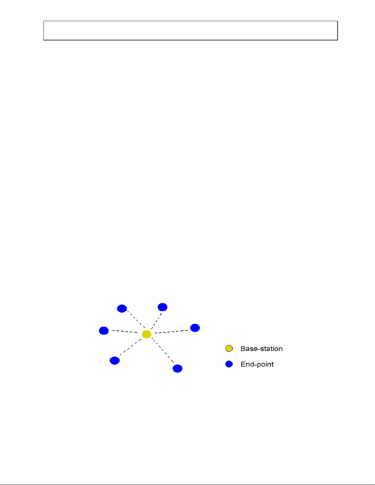
The network topology is a star configuration, as shown in Figure 1. One unit acts as a master unit, usually
referred to as a Base Unit (BS), and all other units are termed End Points (EP). The Base Unit and End Points are
identical in terms of hardware and software.
All communication is between EPs and the BS. It is intended that each EP will operate independent of a PC,
powered from a battery and the BS will be connected to a PC to allow logging of received data. However EPs can
also be connected to a PC to log the transmission success/failure and received data (from the BS). The BS must be
able to hear each EP, but each EP doesn’t necessarily have to hear one another.
Figure 1
The ETSI specific protocol uses non-slotted, non-persistent Carrier Sense Multiple Access with Collision
Avoidance (CSMA-CA). The ETSI bands are duty cycled limited to 10% or less so each EP powers up at regular
intervals to transmit data (e.g. temperature reading). An in-built duty cycle monitor can be used to monitor the
transmit duty cycle. In-between transmissions the EP goes in to a sleep mode. The BS, which is connected to a
PC, is always listening for an EP transmission. The EP listens to the channel before transmitting, thereby
Quick Start Guide Revision 1.0 Page 5 of 22
ADF702X Development Platform
Quick Start Guide ADF702X Development Platform
avoiding collisions. If the channel is assumed clear then the EP begins transmission of the data.
The non-slotted aspect of the protocol means that EPs can transmit as soon as they have data, subject to first
performing a Clear Channel Assessment (CCA). This also ensures no synchronisation is required. The number
of times this back-off can occur is limited, hence the non-persistent nature of the protocol.
The FCC Frequency Hopping (FH) protocol is intended to operate under FCC 15.247 in the 902-928MHz band.
The FH protocol uses 128 hop frequencies with a slot rate of 0.375 seconds. The FH protocol is built on top of the
CSMA-CA protocol meaning that the same CCA and collision avoidance features are used in the FH protocol.
1.3.2 The Hardware
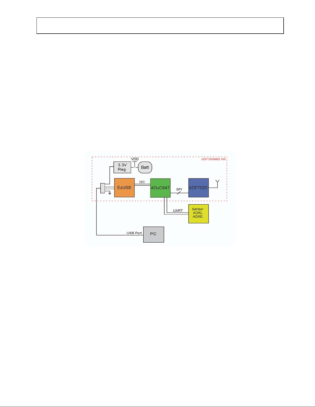
The EVAL-ADF70XX-MB2 controller board is the hardware that ships with the ADF702X Development Kit.
The board consists of a Cypress USB controller, an ADuC847 microconverter, power management, various
interfaces and an RTD. The ADismLINK protocol runs on the ADuC847 microconverter. The RF module
(ADF7020 evaluation board) connects to this controller board and is available separately. The block level
diagram of the hardware is shown in Figure 2.
Figure 2
1.3.3 The Software
The development kit provides two software applications for evaluation and development purposes.
1. ADF7020Demo
This application, written in Visual C++, is used to configure the network. Selection of both the ETSI or
FCC protocol and whether a unit is a BS or EP is allowed. The PHY and MAC layers of each protocol are
largely configurable within the application. The various demonstrations provided with the kit can also be
setup (e.g. temperature sensor network, range testing).
2. ADF7020Registers
This application, also written in C++, is intended for low level configuration of the ADF7020 parameters
and register programming. The application can be used in conjunction with ADF7020Demo to provide
effortless protocol/RF configurability and development.
Quick Start Guide Revision 1.0 Page 6 of 22
ADF702X Development Platform

Quick Start Guide ADF702X Development Platform
3. Source Code
A restricted version of the ADismLINK embedded source code is provided allowing user specific
applications to be easily developed on top of the existing PHY and MAC layers. The Keil C51 compiler is
required for using this code. For assistance/information on developing user specific applications or
using the restricted source code with another compiler, contact our RF & Wireless Components Group
or alternatively contact our Third Party Software Developer, Plextek Ltd., in the UK
(http://www.plextek.com).
Quick Start Guide Revision 1.0 Page 7 of 22
ADF702X Development Platform

Quick Start Guide ADF702X Development Platform
2 Development Kit Setup
2.1 CD Contents
As an install procedure is currently not used, the contents of the CD should be copied to a folder on the host
PC before any setup of the kit is carried out.
2.2 Installing the USB Driver
The files required to install the USB driver are:
CyUSB.sys – the Cypress generic USB driver
•
ADF7020DK.inf – the setup information file
•
•
7DD01xxx.spt – the EZ-USB firmware (the last three digits of the filename represent the version)
These files are located in the folder USB driver which should have been copied to the host PC. Make sure these
files are available ON THE PC, before plugging the board in for the first time.
The development board can be connected to the PC using one of the provided USB cables. At this stage refer to
the document entitled “Installing the USB driver”, which is included in the documentation folder on the CD.
Quick Start Guide Revision 1.0 Page 8 of 22
ADF702X Development Platform

Quick Start Guide ADF702X Development Platform
3 ADF7020Demo.exe
This application is used to select, configure and test the protocol. It allows the user to select either the ETSI duty
cycled protocol or the FCC frequency hopping protocol. All important protocol parameters (PHY and MAC
layers) can then be edited (e.g. number of end points, max payload data) within the software. Several demos are
also provided including a temperature sensor demo and a range-testing demo. These demos allow the user to see
the effect of changing the protocol parameters on the network performance.
The current version of this application is available on the Analog Devices Web Page. The full application name is
ADF7020Demo_VerX.exe, where the X is the current version number.
3.1 Starting ADF7020Demo.exe
Before the application is started the development board should be connected to the PC via the provided USB
cable (ensure switch S2 is selected to ON). If the USB driver has already been installed (Section 2) the driver
should load automatically once the board has been connected. If the USB driver hasn’t been installed then refer
to Section 2.
Run ADF7020Demo.exe from the PC by double clicking on it. Ensure that AdiMACDLL.dll and
DhUsbCommsDLL.dll are in the same location as ADF7020Demo.exe.
Once the executable runs the RPC (method of communication between ADuC847 and PC) initialises and the
RPC and MAC versions appear on the log window as in Figure 3.
Table 1 shows the Software releases and the corresponding RPC and MAC versions.
Software Version RPC version MAC version
Ver1.0 0x16 0x1F
Table 1
Quick Start Guide Revision 1.0 Page 9 of 22
ADF702X Development Platform

Quick Start Guide ADF702X Development Platform
Figure 3
3.2 The GUI
The development kit comes with the code image pre-programmed on the ADuC847. On power up of the board,
the code image looks at a number of locations on the ADuC847 on-board EEprom. This EEprom contains the
ADF7020 configuration parameters as well as all the user-definable protocol parameters and the demo settings.
ADF7020Demo.exe allows the user to edit all values in this EEprom and thus configure the protocol, the RF
parameters and also chose the demo to be run.
3.2.1 Main GUI
To run a demo, a minimum of two development boards and two ADF7020 RF modules are required. One unit
will be configured as a Base Unit and all subsequent units will be configured as End Points using the
ADF7020Demo.exe
On running ADF7020Demo.exe the main GUI appears, as shown in Figure 4.
Quick Start Guide Revision 1.0 Page 10 of 22
ADF702X Development Platform

Quick Start Guide ADF702X Development Platform
Figure 4
3.2.1.1 EEPROM Editor
This allows the user to write to individual addresses in the configuration EEprom. Normally all the EEprom
values are loaded in the Edit Protocol Configuration window (see below), but the EEprom editor allows the user
to both check and edit individual EEprom values without doing a full EEprom load (as is the case in the Edit
Protocol Configuration). This editor is also used when selecting which demo to run as EEprom address 0x0000 is
used to set the demo (see Section 3.3).
3.2.1.2 Transmit Data
This section allows the user to send data from the USB connected unit to another unit (either a Base Unit or End
Point). The address of the intended receiver is placed in Destination Address. The data to be sent can either be
entered in ASCII or Hex. The message can also be set to require an Acknowledge from the destination unit
(select Acknowledged).
Select Transmit to send the message. The option to Log to File is also included here which logs any received
data/error messages to a user specified file. It is also possible to read the transmit duty cycle of the unit connected
to the PC. This is particularly useful in trying to meet the ETSI duty cycled limitations (see the User Manual for
more information on how the duty cycle monitor works).
3.2.1.3 Log Window
All received messages are logged in this window. All transmissions (excluding acknowledges) are also logged in
this window as success/failures.
3.2.1.4 Edit Protocol Configuration
This takes the user to another GUI window which allows full configuration of the protocol and RF parameters
(see the next section).
Quick Start Guide Revision 1.0 Page 11 of 22
ADF702X Development Platform

Quick Start Guide ADF702X Development Platform
3.2.2 Protocol Configuration
On pressing the protocol Configuration Button on the main GUI, the user is taken to the ADF7020 protocol
configuration window. This is shown in Figure 5.
Figure 5
3.2.2.1 Load/Save Configuration
This section of the GUI window allows loading of a preset configuration, saving of a configuration and
downloading of a configuration. The option to save configurations is included due to the number of variable
parameters. The software comes with eight preset configurations which can be loaded using the Load Config File
button. The eight preset configurations are as follows
1. EP_GFSK_10800_ETSI_868
This configuration sets up an End Point using GFSK modulation with a 10.8kbps data rate and 21.6kHz
deviation. Uses the ETSI duty cycled protocol at 868 MHz.
2. BS_GFSK_10800_ETSI_868
This configuration sets up a Base Unit using GFSK modulation with a 10.8kbps data rate and 21.6kHz
deviation. Uses the ETSI duty cycled protocol at 868 MHz.
3. EP_FSK_10800_ETSI_868
Quick Start Guide Revision 1.0 Page 12 of 22
ADF702X Development Platform

Quick Start Guide ADF702X Development Platform
Same as 2 except FSK is used.
4. BS_FSK_10800_ETSI_868
Same as 2 except FSK is used.
5. EP_FSK_2000_ETSI_433
Same as 3 except at 433MHz and 2kbps data rate.
6. BS_FSK_2000_ETSI_433
Same as 4 except at 433MHz and 2kbps data rate.
7. EP_FSK_10800_FCC_FH_915
This configuration sets up an End Point using FSK modulation with a 10.8kbps data rate. Uses the
frequency hopping protocol (FCC 15.247) at 902-928MHz.
8. BS_FSK_10800_FCC_FH_915
This configuration sets up a Base Unit using FSK modulation with a 10.8kbps data rate. Uses the
frequency hopping protocol (FCC 15.247) at 902-928MHz.
All of the above preset configurations can be opened and inspected before downloading to the Configuration
EEprom on the development board. The EEprom is not loaded until the Write to EEprom button is pressed.
Before loading the EEprom all parameters on the GUI can be changed to suit the user’s needs. Alternatively the
user may wish to build up a configuration from scratch, in which case they should refer to the User Manual for
more information on the various tradeoffs and limits on both the MAC and PHY parameters.
3.2.2.2 Receive Register Settings
The Receive Register Settings can be entered for registers 1-6, 9 and 11 of the ADF7020. The register map can be
found on the ADF7020 data sheet. To calculate the register settings it is best to use ADF7020Registers.exe (see
Section 4). It is also possible to save the receive register settings in ADF7020Registers.exe and load them into
ADF7020Demo.exe using the Import Rx Registers button.
3.2.2.3 Transmit Register Settings
It is required to program only 3 registers (register 0, 1 & 2) to set the ADF7020 up in transmit mode (and register
1 is the same in transmit or receive). It is advisable to use the ADF7020 datasheet in conjunction with
ADF7020Register.exe to choose these values. The transmit register values should also correlate with the PHY
parameters.
3.2.2.4 PHY Configuration
This section of the GUI window allows the user to set the various PHY level parameters of the RF link.
Parameters like baud rate, preamble length and RSSI threshold can be set. The PHY parameters chosen here
should correlate with the ADF7020 register settings, as changing them does not automatically update the
register values.
The button Calculate Synth regs will use the xtal frequency, R divider value and base frequency to quickly update
Quick Start Guide Revision 1.0 Page 13 of 22
ADF702X Development Platform

Quick Start Guide ADF702X Development Platform
register 0. The button Calculate PA reg uses the value of PA Level to quickly update register 2. Both these buttons
should just be used to update previously entered values in register 0 & 2.
For further details on the variable parameters in the PHY layer the user is referred to the User Manual. It is
recommended to read the manual before proceeding with altering these parameters from the preset
configurations.
3.2.2.5 MAC Configuration
The MAC section of the GUI window allows the user to set numerous MAC level parameters like frequency
hopping, CSMA and whether the unit is an End Point or Base Unit. Many of these parameters have specific
limits, key trade offs and large implications on the protocol and regulation standards. It is therefore advised to
read the User Manual before attempting to alter these parameters from any of the eight preset configurations.
3.2.3 Loading the Configuration
Once the various settings have been chosen for the board, they must be loaded to the EEprom. This is carried out
by selecting Write to EEPROM which is a button in the Load/Save Configuration section of the GUI window (see
Figure 5).
The user will be asked if they wish to erase the current EEprom values before downloading the new values. It is
recommended to clear the EEprom values.
The EEprom load should take about 4-5 seconds. “Programming entire configuration into EEprom” will appear on
the log window. “Complete” will appear once the EEprom load has finished.
3.3 Running a Demo
Once a board’s EEprom has been loaded with a protocol configuration all that is required is to choose which
demo to run. A demo is selected by editing the value in address 0 of the configuration EEprom. This value is
entered using the EEprom editor (Section 3.2.1.1) on the main GUI window. End Points and Base Units have
different demos, which can be run at the same time.
3.3.1 RPC
RPC stands for Remote Procedure Call. The RPC system is used to allow control of an EP or BS from a PC. It
allows the same interface on the PC as on the target hardware, permitting software to be tested and debugged on
a PC before rebuilding.
On the development board there is an RPC button/switch (S4). If the board is to be connected to the PC and
ADF7020Demo.exe is to be run then the RPC button should be held when powering up the board (i.e.
connecting USB cable).
If the board is just connected to the PC for power or to run ADF7020Registers.exe then the RPC button doesn’t
need to be held on power up.
3.3.2 End Point Demos
The following values can be entered in address 0x0000 of the EEprom to run a particular demo. The EP demos
are independent of whether RPC is on or off.
Quick Start Guide Revision 1.0 Page 14 of 22
ADF702X Development Platform

Quick Start Guide ADF702X Development Platform
Value Demo
0xFFFFFFFF Default Demo: test messages to BS every 5 seconds
0x??000002
0x??000004
0x??000040
0xFF0000??
Test messages to BS every 0x?? seconds
Temperature messages to BS every 0x?? seconds
Persist with the same test packet # when MAC refuses to transmit,
every 0x?? Seconds
Test Message every 5 seconds (either of 3 above demos)
Table 2
3.3.3 Base Unit Demos
The Base unit will only run a demo if RPC is inactive. The demos on the base unit send downlink messages (Base
Unit to End Point Unit). These messages are just test messages with incrementing numbers.
The lower nibble of this test message is displayed on the End Point’s display LEDs. Thus using this demo it is
possible to carry out a range test as both Base Unit and End Point can operate independently of the PC (powered
using supplied battery).
Value RPC Demo
Default Demo: Test Messages to EP #6 and #7 every 20 seconds.
0xFFFFFFFF OFF
0x??000001
OFF
(Range Testing Demo)
Test messages to EP #6 and #7, every 0x?? seconds
(Range Testing Demo)
0xFF0000??
Any ON No Demo
OFF Test Message every 5 seconds (either above 2 demos)
Table 3
3.3.4 Procedure for setting up a demo
Base Unit
1. Connect a board (it is not necessary to have the RF module connected to the development board).
Ensure that the USB drivers have previously been installed.
2. Start ADF7020Demo.exe. Ensure the correct MAC and RPC version load.
3. Enter the Edit Protocol Configuration window by clicking on the button.
4. Load a preset configuration using Load Config File (ensuring it’s a Base Unit configuration). Ensure that
Unit is BS is selected in the MAC parameters.
5. Once the configuration has been finalised, load it to the EEprom by selecting Write to EEprom. Return to
main window by clicking OK. Wait a few seconds (4-5) until Complete appears in the Log Window.
Quick Start Guide Revision 1.0 Page 15 of 22
ADF702X Development Platform

Quick Start Guide ADF702X Development Platform
6. Close ADF7020Demo.exe. Disconnect board.
End Point
1. Connect a board (it is not necessary to have the RF module connected to the development board).
2. Start ADF7020demo.exe. Ensure the correct MAC and RPC version load.
3. Enter the Edit Protocol Configuration window by clicking on the button.
4. Load an EP preset configuration using Load Config File (ensuring it’s the corresponding EP
configuration for the previously loaded BS).
5. Once the configuration has been finalised, load it to the EEprom by selecting Write to EEprom. Return to
main window by clicking OK. Wait a few seconds (4-5) until Complete appears in the Log Window.
6. To tell the development board which demo to run, address 0x0000 of the EEprom must be programmed.
Using the EEprom Editor (see 3.2.1.1), write 0x02000004 to address 0x0000.
7. Close ADF7020Demo.exe. Disconnect Board.
8. Repeat 1-6 for further End Points ensuring each is addressed differently.
Starting Demo
1. Power up each End Point, either from another PC through the USB, a 9V supply or using the supplied
battery. Ensure an ADF7020 RF daughter card is connected to each board. The CPU LED (D5) should
begin to flash.
2. Connect the BS to the PC ensuring that the switch S2 is ON and the RPC button was pressed on power
up.
3. Run ADF7020Demo.exe.
4. Received messages showing the temperature from each EP should begin to appear in the log window.
3.3.5 Log Window Structure
The structure of a received message in the log window is shown in Figure 6.
The first line contains information on the message source address and the Received Signal Strength (RSSI) of the
received signal. The second line gives the first 128 bits in 16x8-bit Hex values. At the end of this line, the ASCII
representation of these values is given.
The second line contains the next 128 bits of the message, displayed as in the first line. As the message shown in
Figure 6 is only 200 bits, the second line displays the remaining 72 bits. The corresponding ASCII values (9
characters) are shown at the end of the line.
Quick Start Guide Revision 1.0 Page 16 of 22
ADF702X Development Platform

Quick Start Guide ADF702X Development Platform
Figure 6
3.3.6 Sample Demo Windows
1. EP #7 temperature message to BS
The Base Unit is connected to the PC with RPC on.
End Point (#7) is stand alone with RPC disabled (battery powered). The demo used was Temperature messages to
BS every 3 seconds (0x03000004 in address 0x0000).
The screen shot of the log window (for the BS, as it’s connected to the PC), is shown in Figure 7.
Figure 7
2. BS Test Message to EP & EP Test Message to BS
End Point #7 is connected to the PC with RPC on. The Demo used was Test Messages to Base Unit every 4
seconds (0x04000004 in address 0x0000).
The Base Unit is stand alone with RPC disabled (battery powered). The demo used was Test messages to EP every
8 seconds (0x08000001 in address 0x0000)
The screen shot of the log window (for the EP, as it’s connected to the PC), is shown in Figure 8.
Quick Start Guide Revision 1.0 Page 17 of 22
ADF702X Development Platform

Quick Start Guide ADF702X Development Platform
Figure 8
3.4 What the development Board LEDs mean
The Development board has numerous LEDs which are highlighted in Figure 9.
1. USB LED
This LED indicates when the board is being supplied with power from the USB. This LED will always
turn on when the development board is connected to a PC via a USB cable.
2. RPC LED
This LED indicates when information is being sent to the PC via the USB. Also if a board is being
powered from the USB but RPC is off this light will remain ON.
3. Power LED
This LED indicates when power is being supplied to the board.
4. CPU LED
This LED indicates when the MAC running on the ADuC847 is awake.
5. Display LEDs
These four LEDs are tied to the lower nibble of the ADuC847 GPIO port P0. Depending on whether the
unit is a base unit or an End Point and on various other protocol/demo settings these LEDs have
different functions. A full explanation of their purpose is given in the User Manual.
Quick Start Guide Revision 1.0 Page 18 of 22
ADF702X Development Platform

Quick Start Guide ADF702X Development Platform
Figure 9
Quick Start Guide Revision 1.0 Page 19 of 22
ADF702X Development Platform

Quick Start Guide ADF702X Development Platform
4 ADF7020Registers.exe
This application allows low level configuration of the ADF7020, by calculating the parts register settings and
downloading of these settings through the USB. The application can be used either as calculation tool to check
register values without downloading them to the ADF7020, or simply as a method of programming the ADF7020
and doing low-level (e.g. BER, data rate, modulation type) device evaluation.
ADF7020Registers.exe may also be opened at the same time as ADF7020Demo.exe, which is helpful when setting
up the ADF7020 register values in the protocol configuration window.
The full application name is ADF7020Registers_VerX.exe, where the X is the current version number.
4.1 Using ADF7020Registers.exe
To use ADF7020Registers as a low level configuration tool for the ADF7020 settings, independent of any
protocol then the protocol will have to be first disabled. To do this use the EEprom Editor tool in
ADF7020Demo.exe and program address 0x0000 with 0x000000FF.
EEprom Address EEprom Value Function
0x0004 0x000000FF Protocol deactivated and demos disabled. Use
this configuration with ADF7020Registers.exe
Table 4
4.2 The GUI
The main GUI window is shown in Figure 10. If the application is just to be used as a register calculator (e.g. with
ADF7020Demo.exe) then Connect USB should NOT be pressed. The Connect USB button (in the top RHS of the
GUI) should be pressed if a development board with an ADF7020 RF module is connected to the PC via the USB
and the user wishes to program the ADF7020 registers. When the button is pressed the RPC and MAC version
should appear in the Connected box at the top of the GUI.
Quick Start Guide Revision 1.0 Page 20 of 22
ADF702X Development Platform

Quick Start Guide ADF702X Development Platform
Figure 10
After selecting Transmit (Tx) or Receive (Rx) mode, you can select the required modulation scheme by clicking
on the drop-down box in the Modulation Options section.
The GUI window is divided up into several sections some of which have their own sub-windows which are
indicated by a raised button. For example in the Modulation Options section, one can enter the sub-window by
clicking on the AFC/Advanced button.
In the FSK panel you should enter the deviation frequency, data-rate, demodulation type and IF Bandwidth. In
Rx mode all the appropriate clock frequencies are chosen for you based on these inputs. You will need to click on
the AFC/Advanced button to force the software to auto-calculate these clock frequencies which will be displayed
on the AFC/Advanced sub-window.
Another feature of the software is to display the output of the Readback pin on the ADF7020 (see the Readback
section in ADF7020 Datasheet for more details). This can display the battery voltage, temperature and external
ADC input or frequency error.
For direct programming of the ADF7020, values can be entered manually (in hex) into the register boxes at the
bottom of the screen. To upload the current values in the register boxes, the user must either select Update 0-6 or
update each register individually.
Quick Start Guide Revision 1.0 Page 21 of 22
ADF702X Development Platform

Quick Start Guide ADF702X Development Platform
5 Using the Application software with other ADF702X Modules
Both ADF7020Demo.exe and ADF7020Registres.exe are specifically intended for the ADF7020. It is intended in
future releases of the application software to incorporate the ADF7025 and other ADF702X devices.
However the development kit can still currently be used with other ADF702X devices, once the user takes into
account some considerations.
5.1 ADF7020Demo.exe with another ADF702X Module
The protocol will operate independent of which ADF702x device is connected, but the application software will
not. The main consideration is that each ADF702X device may have slightly different register maps. To use the
ADF7020Demo.exe application to set up a network with an ADF702X device other than the ADF7020 one should
use the following steps:
1. Connect the development board (with attached ADF702X device) to the PC via the USB. Run the
ADF7020Demo.exe.
2. Enter the protocol configuration window. Using the ADF702X Data Sheet, the user should then calculate
the correct Receive and Transmit register settings for their RF link. These should be directly entered into
the available spaces for each register value on the GUI window.
3. In the PHY section of the GUI, the correct parameters should be entered but Calc Synth Regs and Calc
PA Reg should not be pressed (as this will change the register values).
4. Enter the MAC parameters as normal.
5. Save the configuration and name it appropriately, so that the configuration is available for future use.
6. Load the configuration to the EEprom by selecting Write to EEPROM.
7. Click OK and wait for 4-5 seconds for Complete to appear in the Log window.
For each unit, be it End Point or Base Unit this procedure should be followed.
Quick Start Guide Revision 1.0 Page 22 of 22
ADF702X Development Platform
 Loading...