A
io-homecontrol-Compliant RF Transceiver
FEATURES
Very low power, high performance, low IF transceiver
Fully integrated io-homecontrol compliant protocol covering
Layer 1, Layer 2, and time critical elements of Layer 3
Media access
Master, slave, and beacon modes supported
Automatic io-homecontrol channel scan
Automatic CRC, preamble, start byte insertion/check
UART data encoding as per io-homecontrol
Smart preamble detect/packet sniffing
Automatic address filtering
Low power modes
Autonomous packet handling without intervention of host
microprocessor thus significantly increasing battery life
1-way and 2-way communication supported
Automatic wake-up timer
32-bit hardware timer, 16-bit firmware timer (48 bits total)
Uses either
External 32 kHz crystal
Internal 32 kHz RC oscillator
Patented fast settling automatic frequency control (AFC)
Fully integrated image rejection calibration (patent pending)
Digital RSSI
Operating frequencies
Channel 1: 868.25 MHz
Channel 2: 868.95 MHz
Channel 3: 869.85 MHz
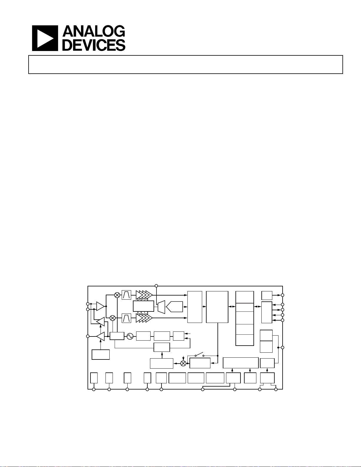
FUNCTIONAL BLOCK DIAGRAM
DCIN_ATB3
ADF7022
Very low power consumption
12.8 mA in receive mode with AGC active
11.9 mA in receive mode with manual AGC, ADC off
24.1 mA in transmit mode (10 dBm output)
0.75 μA in RCO wake mode
1.25 μA in XTO wake mode (32 kHz oscillator active)
38.4 μA average current in low power mode
Receiver sensitivity (10
−108.5 dBm at 38.4 kbps FSK, 20 kHz deviation
Output power programmable up to 13.5 dBm
Automatic PA ramping
Dual PAs offer Tx antenna diversity
Very few external components
Integrated PLL loop filter
Integrated Rx/Tx switch
Integrated battery monitor
On-chip 8-bit ADC and temperature sensor
Efficient and flexible SPI control interface
4 lines available for low cost microcontroller interface
Flexible Tx and Rx data buffers
Efficient burst mode register access
1.8 V to 3.6 V power supply
5 mm × 5 mm, 32-lead LFCSP package
APPLICATIONS
Home automation
Process and building control
−3
BER)
FSK
RFIO_1 P
RFIO_1N
RFO2
LNA
PA
PA
PA RAMP
PROFILE
DIVIDER
ADF7022
LDO2
LDO1
1
GPIO REFERS TO PIN G P0 TO PIN GP5.
RSSI/
LOGAMP
LOOP
FILTER
LDO3
CHARGE
PUMP
DIVIDER
Σ-∆
MODULATOR
BIAS
LDO4
MUX
ANALOG
8-BIT
ADC
TEST
DEMOD
PF
D
f
DEV
SENSOR
CDR
AFC
AGC
GAUSSIAN
FILTER
TEMP
8-BIT RISC
PROCESSOR
BATTERY
MONITOR
Figure 1.
For more information on the ADF7022, contact a local sales office at Analog Devices, Inc.
Rev. SpA
Information furnished by Analog Devices is believed to be accurate and reliable. However, no
responsibility is assumed by Anal og Devices for its use, nor for any infringements of patents or ot her
rights of third parties that may result from its use. Specifications subject to change without notice. No
license is granted by implication or otherwise under any patent or patent rights of Analog Devices.
Trademarks and registered trademarks are the property of their respective owners.
One Technology Way, P.O. Box 9106, Norwood, MA 02062-9106, U.S.A.
Tel: 781.329.4700 www.analog.com
Fax: 781.461.3113 ©2009–2011 Analog Devices, Inc. All rights reserved.
4kB ROM
IO-H/C
MAC
2kB RAM
256-BYTE
PACKET
RAM
64-BYTE
BBRAM
256-BYTE
MCR RAM
WAKE UP CONTROL
TIMER UNI T
32kHz
32kHz
RCOSC
OSC
IRQ
CTRL
SPI
GPIO
TEST
DAC
CLOCK
DIVIDER
26MHz
OSC
XOSC26N XOSC26PXOSC32KP_GP5_ATB1XOSC32KN_A TB2RBIASCREGRFx CREGVCO CREGSYNTH CREGDIGx
IRQ_GP3
CSN
MISO
SCLK
MOSI
1
GPIO
08266-001

ADF7022
NOTES
©2009–2011 Analog Devices, Inc. All rights reserved. Trademarks and
registered trademarks are the property of their respective owners.
D08266F-0-2/11(SpA)
Rev. SpA | Page 2 of 2
 Loading...