

High Performance,
R
FEATURES
High performance, low power, narrow-band transceiver
Enhanced performance ADF7021-N with external VCO
Frequency bands using external VCO: 80 MHz to 960 MHz
Improved adjacent channel power (ACP) and adjacent
channel rejection (ACR) compared with the ADF7021-N
Programmable IF filter bandwidths: 9 kHz, 13.5 kHz,
and 18.5 kHz
Modulation schemes: 2FSK, 3FSK, 4FSK, MSK
Spectral shaping: Gaussian and raised cosine filtering
Data rates: 0.05 kbps to 24 kbps
Power supply: 2.3 V to 3.6 V
Programmable output power: −16 dBm to +13 dBm
in 63 steps
Automatic power amplifier (PA) ramp control
Receiver sensitivity
−125 dBm at 250 bps, 2FSK
−122 dBm at 1 kbps, 2FSK
Patent pending, on-chip image rejection calibration
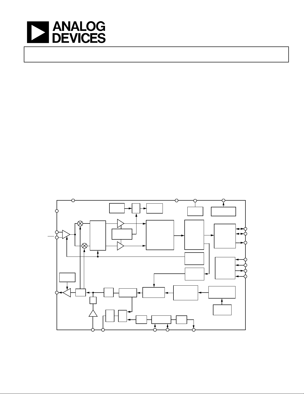
FUNCTIONAL BLOCK DIAGRAM
RSET
Narrow-Band Transceiver IC
ADF7021-V
On-chip fractional-N PLL
On-chip, 7-bit ADC and temperature sensor
Fully automatic frequency control (AFC) loop
Digital received signal strength indication (RSSI)
Integrated Tx/Rx switch
Leakage current in power-down mode: 0.1 μA
APPLICATIONS
Narrow-band, short-range device (SRD) standards
ETSI EN 300 220
500 mW output power capability in 869 MHz g3 subband
with external PA
High performance receiver rejection, blocking, and
adjacent channel power (ACP)
FCC Part 90 (meets Emission Mask D requirements)
FCC Part 95
ARIB STD-T67
Wireless metering
Narrow-band wireless telemetry
EG[1:4]CE
C
MUXOUT
R
LNA
RFIN
RFIN
RFOUT
LNA
GAIN
PA RAMP
÷1/÷2
BUFFER
IF FILTER
÷2
L2
DIV P
CPOUT
TEMP
SENSOR
LOG AMP
ADF7021-V
CP
RSSI/
PFD
N/N + 1
MUX
MODULATOR
DIV R
7-BIT ADC
2FSK
3FSK
4FSK
DEMODULATOR
Σ-Δ
OSC
OSC1 OSC2
LDO[1:4]
CLOCK
AND DATA
RECOVERY
AGC
CONTROL
AFC
CONTROL
2FSK
3FSK
4FSK
MOD CONTROL
CLK
DIV
CLKOUT
TEST MUX
Tx/Rx
CONTROL
SERIAL
PORT
GAUSSIAN/
RAISED COSINE
FILTER
3FSK
ENCODING
TxRxCLK
TxRxDATA
SWD
SLE
SDATA
SREAD
SCLK
8635-001
Figure 1.
Rev. 0
Information furnished by Analog Devices is believed to be accurate and reliable. However, no
responsibility is assumed by Analog Devices for its use, nor for any infringements of patents or other
rights of third parties that may result from its use. Specifications subject to change without notice. No
license is granted by implication or otherwise under any patent or patent rights of Analog Devices.
Trademarks and registered trademarks are the property of their respective owners.
One Technology Way, P.O. Box 9106, Norwood, MA 02062-9106, U.S.A.
Tel: 781.329.4700 www.analog.com
Fax: 781.461.3113 ©2010 Analog Devices, Inc. All rights reserved.

ADF7021-V
TABLE OF CONTENTS
Features .............................................................................................. 1
Applications ....................................................................................... 1
Functional Block Diagram .............................................................. 1
Revision History ............................................................................... 2
General Description ......................................................................... 3
Specifications ..................................................................................... 4
RF and PLL Specifications ........................................................... 4
Transmission Specifications ........................................................ 5
Receiver Specifications ................................................................ 6
Digital Specifications ................................................................... 9
General Specifications ............................................................... 10
Timing Characteristics .............................................................. 10
Timing Diagrams ........................................................................ 11
Absolute Maximum Ratings .......................................................... 14
ESD Caution ................................................................................ 14
Pin Configuration and Function Descriptions ........................... 15
Typical Performance Characteristics ........................................... 17
Frequency Synthesizer ................................................................... 21
Reference Input ........................................................................... 21
MUXOUT .................................................................................... 22
Voltage Controlled Oscillator (VCO) ...................................... 23
Choosing a VCO for Best System Performance ..................... 23
Transmitter ...................................................................................... 24
RF Output Stage .......................................................................... 24
Modulation Schemes .................................................................. 24
Spectral Shaping ......................................................................... 26
Modulation and Filtering Options ........................................... 27
Transmit Latency ........................................................................ 27
Test Pattern Generator ............................................................... 27
Receiver Section .............................................................................. 28
RF Front End ............................................................................... 28
IF Filter ......................................................................................... 28
RSSI/AGC .................................................................................... 28
Demodulation, Detection, and CDR ....................................... 30
Receiver Setup ............................................................................. 32
FSK Demodulator Optimization .............................................. 33
AFC Operation ........................................................................... 34
Automatic Sync Word Detection (SWD) ................................ 35
Applications Information .............................................................. 36
IF Filter Bandwidth Calibration ............................................... 36
LNA/PA Matching ...................................................................... 37
Image Rejection Calibration ..................................................... 38
Packet Structure and Coding .................................................... 39
Programming After Initial Power-Up ..................................... 39
Applications Circuit ................................................................... 42
Serial Interface ................................................................................ 43
Readback Format ........................................................................ 43
Interfacing to a Microcontroller/DSP ..................................... 44
Register 0—N Register ............................................................... 45
Register 1—Oscillator Register ................................................. 46
Register 2—Transmit Modulation Register ............................ 47
Register 3—Transmit/Receive Clock Register ........................ 48
Register 4—Demodulator Setup Register ............................... 49
Register 5—IF Filter Setup Register ......................................... 50
Register 6—IF Fine Calibration Setup Register ..................... 51
Register 7—Readback Setup Register ...................................... 52
Register 8—Power-Down Test Register .................................. 53
Register 9—AGC Register ......................................................... 54
Register 10—AFC Register ....................................................... 55
Register 11—Sync Word Detect Register ................................ 56
Register 12—SWD/Threshold Setup Register ........................ 56
Register 13—3FSK/4FSK Demodulation Register ................. 57
Register 14—Test DAC Register ............................................... 58
Register 15—Test Mode Register ............................................. 59
Outline Dimensions ....................................................................... 60
Ordering Guide .......................................................................... 60
REVISION HISTORY
4/10—Revision 0: Initial Version
Rev. 0 | Page 2 of 60

ADF7021-V
GENERAL DESCRIPTION
The ADF7021-V is a high performance, low power, narrow-band
RF transceiver based on the ADF7021-N. The architecture of
the ADF7021-V transceiver is similar to that of the ADF7021-N
except that an external VCO is used by the on-chip RF synthesizer
for applications that require improved phase noise performance.
The ADF7021-V is designed to operate in both the license-free
ISM bands and in the licensed bands from 80 MHz to 960 MHz.
To minimize RF feedthrough and spurious emissions, the
external VCO operates at 2× or 4× the desired RF frequency;
the ADF7021-V supports a maximum VCO frequency operation
of 1920 MHz. The 4× VCO operation is programmable by
enabling an additional on-chip divide-by-2 outside the RF
synthesizer loop and offers improved phase noise performance.
As with the ADF7021-N receiver, the IF filter bandwidths
of 9 kHz, 13.5 kHz, and 18.5 kHz are supported, making the
ADF7021-V ideally suited to worldwide narrow-band telemetry
applications.
The part has both Gaussian and raised cosine transmit data
filtering options to improve spectral efficiency for narrow-band
applications. It is suitable for circuit applications targeted at the
following:
• European ETSI EN 300 220
• North American FCC Part 15, Part 90, and Part 95
• Japanese ARIB STD-T67
• Korean short-range device regulations
• Chinese short-range device regulations
A complete transceiver can be built using a small number of
discrete external components, making the ADF7021-V very
suitable for area-sensitive, high performance driven applications.
The range of on-chip FSK modulation and data filtering options
allows users greater flexibility in their choice of modulation
schemes while meeting the tight spectral efficiency requirements.
The ADF7021-V also supports protocols that dynamically switch
among 2FSK, 3FSK, and 4FSK to maximize communication
range and data throughput.
The transmit section contains a low noise fractional-N PLL with
an output resolution of <1 ppm. The frequency-agile PLL allows
the ADF7021-V to be used in frequency-hopping spread spectrum
(FHSS) systems. The VCO is external, which provides better
phase noise and thus lower adjacent channel power (ACP) and
adjacent channel rejection (ACR) compared with the ADF7021-N.
The VCO tuning range extends from 0.2 V to 2 V, which should
be taken into account when choosing the external VCO.
The transmitter output power is programmable in 63 steps from
−16 dBm to +13 dBm and has an automatic power amplifier ramp
control to prevent spectral splatter and help meet regulatory
standards. The transceiver RF frequency, channel spacing, and
modulation are programmable using a simple 3-wire interface.
The device operates with a power supply range of 2.3 V to 3.6 V
and can be powered down when not in use.
A low IF architecture is used in the receiver (100 kHz), which
minimizes power consumption and the external component
count yet avoids dc offset and flicker noise at low frequencies.
The IF filter has programmable bandwidths of 9 kHz, 13.5 kHz,
and 18.5 kHz. The ADF7021-V supports a wide variety of programmable features, including Rx linearity, sensitivity, and IF
bandwidth, allowing the user to trade off receiver sensitivity
and selectivity against current consumption, depending on
the application. The receiver also features a patented automatic
frequency control (AFC) loop with programmable pull-in range
that allows the PLL to remove the frequency error in the
incoming signal.
The receiver achieves an image rejection performance of 50 dB
using a patent-pending IR calibration scheme that does not
require the use of an external RF source.
An on-chip ADC provides readback of the integrated temperature sensor, external analog input, battery voltage, and RSSI
signal, which can eliminate the need for an external ADC in
some applications. The temperature sensor is accurate to ±10°C
over the full operating temperature range of −40°C to +85°C.
This accuracy can be improved by performing a one-point calibration at room temperature and storing the result in memory.
Rev. 0 | Page 3 of 60

ADF7021-V
SPECIFICATIONS
VDD = 2.3 V to 3.6 V, GND = 0 V, TA = T
measurements are performed with the EVAL-ADF7021-VDBxZ using the PN9 data sequence, unless otherwise noted. The version
number of ETSI EN 300 200-1 is V2.3.1. LBW = loop bandwidth and IFBW = IF filter bandwidth.
RF AND PLL SPECIFICATIONS
Table 1.
Parameter Min Typ Max Unit Test Conditions/Comments
RF CHARACTERISTICS
Phase Frequency Detector (PFD)
Frequenc y
PHASE-LOCKED LOOP (PLL)
Normalized In-Band Phase Noise
1
Floor
PLL Settling 155 μs
EXTERNAL VCO
Tuning Range 0.2 2 V
Pin L2 Input Sensitivity 0 dBm VCO frequency < 1920 MHz
REFERENCE INPUT
Crystal Reference
External Oscillator
Crystal Start-Up Time
XTAL Bias = 20 μA 0.930 ms
XTAL Bias = 35 μA 0.438 ms
Input Level for External Oscillator
OSC1 Pin 0.8 V p-p Clipped sine wave
OSC2 Pin CMOS levels V
ADC PARAMETERS VDD = 2.3 V to 3.6 V, TA = 25°C
Integral Nonlinearity (INL) ±0.4 LSB
Differential Nonlinearity (DNL) ±0.4 LSB
1
This value can be used to calculate the in-band phase noise for any operating frequency. Use the following equation to calculate the in-band phase noise performance
as seen at the power amplifier (PA) output: −203 + 10 log(f
2
Guaranteed by design. Sample tested to ensure compliance.
3
A TCXO, VCXO, or OCXO can be used as an external oscillator.
4
Crystal start-up time is the time from chip enable (CE) being asserted to correct clock frequency on the CLKOUT pin.
2
2, 3
3.625 24 MHz
4
to T
MIN
RF/256 24 MHz
, unless otherwise noted. Typical specifications are at VDD = 3 V, TA = 25°C. All
MAX
Maximum usable PFD at a particular RF frequency
is limited by the minimum N divider value
−203 dBc/Hz
Measured for a 100 kHz frequency step to within
5 ppm accuracy, PFD = 19.68 MHz, LBW = 8 kHz
3.625 24 MHz
10 MHz XTAL, 33 pF load capacitors, VDD = 3.0 V
) + 20 logN.
PFD
Rev. 0 | Page 4 of 60

ADF7021-V
TRANSMISSION SPECIFICATIONS
LBW = loop bandwidth.
Table 2.
Parameter Min Typ Max Unit Test Conditions/Comments
DATA RATE Limited by the loop bandwidth
2FSK 0.05 18.5 kbps LBW must be ≥1.25 × data rate for correct operation
3FSK 0.05 18.5 kbps LBW = 18.5 kHz
4FSK 0.05 24 kbps LBW = 18.5 kHz
MODULATION
Frequency Deviation (f
0.306 156 kHz PFD = 20 MHz
Frequency Deviation Resolution 56 Hz PFD = 3.625 MHz
Gaussian Filter Bandwidth Time (BT) 0.5
Raised Cosine Filter Alpha 0.5/0.7 Programmable
TRANSMIT POWER
Maximum Transmit Power
Transmit Power Variation vs.
Temperature
Transmit Power Variation vs. VDD ±1 dB VDD = 2.3 V to 3.6 V at 915 MHz, TA = 25°C
Transmit Power Flatness ±1 dB 902 MHz to 928 MHz, VDD = 3 V, TA = 25°C
Programmable Step Size 0.3125 dB −16 dBm to +13 dBm
ADJACENT CHANNEL POWER (ACP)
460 MHz
12.5 kHz Channel Spacing −47 dBm
25 kHz Channel Spacing −53 dBm
868 MHz Compliant with ETSI EN 300 220
12.5 kHz Channel Spacing −44 dBm
25 kHz Channel Spacing −49 dBm
MODULATION BANDWIDTH
125 kHz Offset −74.5 dBm/1 kHz
125 kHz + 200 kHz −79 dBm/1 kHz
125 kHz + 400 kHz −69.5 dBm/10 kHz
125 kHz + 1 MHz −62 dBm/100 kHz
EMISSION MASK
12.5 kHz Offset
460 MHz −77 dBc
OCCUPIED BANDWIDTH
2FSK, Gaussian Data Filtering
12.5 kHz Channel Spacing 4.0 kHz 2.4 kbps PN9 data, f
25 kHz Channel Spacing 8.5 kHz 4.8 kbps PN9 data, f
2FSK, Raised Cosine Data Filtering
12.5 kHz Channel Spacing 4.5 kHz 2.4 kbps PN9 data, f
25 kHz Channel Spacing 9.6 kHz 4.8 kbps PN9 data, f
) 0.056 28.26 kHz PFD = 3.625 MHz
DEV
1
13 dBm VDD = 3.0 V, TA = 25°C
±1 dB T
= −40°C to +85°C
A
Gaussian 2FSK modulation, 13 dBm output power,
PFD = 19.68 MHz, LBW = 6 kHz
Measured in a ±8.5 kHz bandwidth at ±12.5 kHz
offset, 2.4 kbps PN9 data, f
Measured in a ±16 kHz bandwidth at ±25 kHz
offset, 4.8 kbps PN9 data, f
Measured in a ±8.5 kHz bandwidth at ±12.5 kHz
offset, 2.4 kbps PN9 data, f
Measured in a ±16 kHz bandwidth at ±25 kHz
offset, 4.8 kbps PN9 data, f
869.525 MHz, Gaussian 2FSK modulation, 4.8 kbps,
f
= 2.4 kHz, 10 dBm output power,2 compliant
DEV
with ETSI EN 300 220, LBW = 6 kHz
FCC Part 90 Emission Mask D, 100 Hz resolution
bandwidth, Gaussian 2FSK modulation, LBW =
6 kHz, 10 dBm output power, 2.4 kbps PN9 data,
= 1.2 kHz
f
DEV
99.0% of total mean power, LBW = 6 kHz, 10 dBm
output power
= 1.2 kHz
DEV
= 2.4 kHz
DEV
= 1.2 kHz
DEV
= 2.4 kHz
DEV
= 1.2 kHz
DEV
= 2.4 kHz
DEV
= 1.2 kHz
DEV
= 2.4 kHz
DEV
Rev. 0 | Page 5 of 60

ADF7021-V
Parameter Min Typ Max Unit Test Conditions/Comments
3FSK, Raised Cosine Filtering
12.5 kHz Channel Spacing 4.3 kHz 2.4 kbps PN9 data, f
25 kHz Channel Spacing 8.5 kHz 4.8 kbps PN9 data, f
4FSK, Raised Cosine Filtering
25 kHz Channel Spacing 11.3 kHz 9.6 kbps PN9 data, f
SPURIOUS EMISSIONS
Reference Spurs −65 dBc LBW = 8 kHz
HARMONICS
3
13 dBm output power
Second Harmonic −35/−52 dBc Unfiltered conductive/filtered conductive
Third Harmonic −43/−60 dBc Unfiltered conductive/filtered conductive
All Other Harmonics −36/−65 dBc Unfiltered conductive/filtered conductive
OPTIMUM PA LOAD IMPEDANCE
fRF = 915 MHz 39 + j61 Ω
fRF = 868 MHz 48 + j54 Ω
fRF = 470 MHz 97.5 + j64.4 Ω
fRF = 450 MHz 98 + j65 Ω
fRF = 426 MHz 100 + j65 Ω
fRF = 315 MHz 129 + j63 Ω
fRF = 175 MHz 173 + j49 Ω
fRF = 169 MHz 74.5 + j48.5 Ω
1
Measured as maximum unmodulated power.
2
Suitable for ETSI 500 mW Tx requirements.
3
Conductive filtered harmonic emissions measured on the EVAL-ADF7021-VDBxZ, which includes a T-stage harmonic filter (two inductors and one capacitor).
= 1.2 kHz
DEV
= 2.4 kHz
DEV
= 1.2 kHz
DEV
RECEIVER SPECIFICATIONS
LBW = loop bandwidth and IFBW = IF filter bandwidth.
Table 3.
Parameter Min Typ Max Unit Test Conditions/Comments
DATA RATE Limited by the IF filter bandwidth
2FSK 0.05 9.0 kbps IFBW = 9 kHz
0.05 13.5 kbps IFBW = 13.5 kHz
0.05 18.5 kbps IFBW = 18.5 kHz
3FSK 0.05 18.5 kbps IFBW = 18.5 kHz
4FSK 0.05 24 kbps IFBW = 18.5 kHz
SENSITIVITY Bit error rate (BER) = 10−3
2FSK
Sensitivity at 0.25 kbps −125 dBm f
Sensitivity at 1 kbps −122 dBm f
Sensitivity at 2.4 kbps −119 dBm f
Sensitivity at 4.8 kbps −116 dBm f
Sensitivity at 9.6 kbps −114 dBm f
= 1 kHz, high sensitivity mode, IFBW = 9.0 kHz
DEV
= 1 kHz, high sensitivity mode, IFBW = 9.0 kHz
DEV
= 1.2 kHz, high sensitivity mode, IFBW = 9.0 kHz
DEV
= 2.4 kHz, high sensitivity mode, IFBW = 9.0 kHz
DEV
= 4.8 kHz, high sensitivity mode, IFBW = 18.5 kHz
DEV
Gaussian 2FSK
Sensitivity at 0.25 kbps −125 dBm f
Sensitivity at 1 kbps −122 dBm f
Sensitivity at 2.4 kbps −120 dBm f
Sensitivity at 4.8 kbps −117 dBm f
Sensitivity at 9.6 kbps −114 dBm f
= 1 kHz, high sensitivity mode, IFBW = 9.0 kHz
DEV
= 1 kHz, high sensitivity mode, IFBW = 9.0 kHz
DEV
= 1.2 kHz, high sensitivity mode, IFBW = 9.0 kHz
DEV
= 2.4 kHz, high sensitivity mode, IFBW = 9.0 kHz
DEV
= 4.8 kHz, high sensitivity mode, IFBW = 18.5 kHz
DEV
GMSK
Sensitivity at 4.8 kbps −114.5 dBm f
= 1.2 kHz, high sensitivity mode, IFBW = 9.0 kHz
DEV
1
Rev. 0 | Page 6 of 60

ADF7021-V
Parameter Min Typ Max Unit Test Conditions/Comments
Raised Cosine 2FSK
Sensitivity at 0.25 kbps −125 dBm f
Sensitivity at 1 kbps −121 dBm f
Sensitivity at 2.4 kbps −120 dBm f
Sensitivity at 4.8 kbps −115 dBm f
Sensitivity at 9.6 kbps −114 dBm f
3FSK
Sensitivity at 4.8 kbps −110 dBm
Raised Cosine 3FSK
Sensitivity at 4.8 kbps −110 dBm
4FSK
Sensitivity at 4.8 kbps −112 dBm
Raised Cosine 4FSK
Sensitivity at 4.8 kbps −109 dBm
INPUT IP3
Low Gain, Enhanced Linearity
−3 dBm LNA_GAIN = 3, MIXER_LINEARITY = 1
Mode
Medium Gain Mode −13.5 dBm LNA_GAIN = 10, MIXER_LINEARITY = 0
High Sensitivity Mode −24 dBm LNA_GAIN = 30, MIXER_LINEARITY = 0
ADJACENT CHANNEL REJECTION
(ACR)
868 MHz
12.5 kHz Channel Spacing −60 dBm IFBW = 9 kHz, data rate = 0.25 kbps, f
25 kHz Channel Spacing −39 dBm IFBW = 9 kHz, data rate = 0.25 kbps, f
12.5 kHz Channel Spacing −60 dBm IFBW = 9 kHz, data rate = 1 kbps, f
25 kHz Channel Spacing −40 dBm IFBW = 9 kHz, data rate = 1 kbps, f
12.5 kHz Channel Spacing −59.5 dBm IFBW = 9 kHz, data rate = 2.4 kbps, f
25 kHz Channel Spacing −42 dBm IFBW = 9 kHz, data rate = 2.4 kbps, f
12.5 kHz Channel Spacing −63 dBm IFBW = 9 kHz, data rate = 4.8 kbps, f
25 kHz Channel Spacing −45 dBm IFBW = 9 kHz, data rate = 4.8 kbps, f
25 kHz Channel Spacing −57 dBm IFBW = 18.5 kHz, data rate = 9.6 kbps, f
460 MHz
12.5 kHz Channel Spacing −59.5 dBm IFBW = 9 kHz, data rate = 0.25 kbps, f
25 kHz Channel Spacing −37.5 dBm IFBW = 9 kHz, data rate = 0.25 kbps, f
12.5 kHz Channel Spacing −60 dBm IFBW = 9 kHz, data rate = 1 kbps, f
25 kHz Channel Spacing −41 dBm IFBW = 9 kHz, data rate = 1 kbps, f
12.5 kHz Channel Spacing −62 dBm IFBW = 9 kHz, data rate = 2.4 kbps, f
25 kHz Channel Spacing −43 dBm IFBW = 9 kHz, data rate = 2.4 kbps, f
12.5 kHz Channel Spacing −61.5 dBm IFBW = 9 kHz, data rate = 4.8 kbps, f
25 kHz Channel Spacing −44.5 dBm IFBW = 9 kHz, data rate = 4.8 kbps, f
25 kHz Channel Spacing −56 dBm IFBW = 18.5 kHz, data rate = 9.6 kbps, f
COCHANNEL REJECTION
868 MHz −5 dB IFBW = 9 kHz, data rate = 4.8 kbps, f
= 1 kHz, high sensitivity mode, IFBW = 9.0 kHz
DEV
= 1 kHz, high sensitivity mode, IFBW = 9.0 kHz
DEV
= 1.2 kHz, high sensitivity mode, IFBW = 9.0 kHz
DEV
= 2.4 kHz, high sensitivity mode, IFBW = 9.0 kHz
DEV
= 4.8 kHz, high sensitivity mode, IFBW = 18.5 kHz
DEV
= 2.4 kHz, high sensitivity mode, IFBW = 18.5 kHz,
f
DEV
Viterbi detection on
= 2.4 kHz, high sensitivity mode, IFBW = 13.5 kHz,
f
DEV
alpha = 0.5, Viterbi detection on
(inner)2 = 1.2 kHz, high sensitivity mode, IFBW = 13.5
f
DEV
kHz
(inner)2 = 1.2 kHz, high sensitivity mode, IFBW = 13.5 kHz,
f
DEV
alpha = 0.5
Two-tone test, f
− 800 kHz
f2 = f
LO
= 860 MHz, f1 = fLO + 100 kHz,
LO
Desired signal is 3 dB above the sensitivity point of
−109.5 dBm as per EN 300 220; rejection is measured as the
level of an unmodulated interferer to cause a BER of 10
−2
for
the desired signal
= 1 kHz, LBW = 6 kHz
DEV
= 1 kHz, LBW = 6 kHz
DEV
= 1 kHz, LBW = 6 kHz
DEV
= 1 kHz, LBW = 6 kHz
DEV
= 1.2 kHz, LBW = 6 kHz
DEV
= 1.2 kHz, LBW = 6 kHz
DEV
= 2.4 kHz, LBW = 6 kHz
DEV
= 2.4 kHz, LBW = 6 kHz
DEV
= 4.8 kHz, LBW = 6 kHz
DEV
Desired signal is at −106.5 dBm; rejection is measured as the
level of an unmodulated interferer to cause a BER of 10
−2
for
the desired signal
= 1 kHz, LBW = 6 kHz
DEV
= 1 kHz, LBW = 6 kHz
DEV
= 1 kHz, LBW = 6 kHz
DEV
= 1 kHz, LBW = 6 kHz
DEV
= 1.2 kHz, LBW = 6 kHz
DEV
= 1.2 kHz, LBW = 6 kHz
DEV
= 2.4 kHz, LBW = 6 kHz
DEV
= 2.4 kHz, LBW = 6 kHz
DEV
= 4.8 kHz, LBW = 6 kHz
DEV
Desired signal is 3 dB above the sensitivity point of
−109.5 dBm; rejection is measured as the level of an
interferer to cause a BER of 10
−2
for the desired signal
= 2.4 kHz, LBW = 6 kHz
DEV
Rev. 0 | Page 7 of 60

ADF7021-V
Parameter Min Typ Max Unit Test Conditions/Comments
IMAGE CHANNEL REJECTION
868 MHz 26/39 dB Uncalibrated/calibrated,3 VDD = 3.0 V, TA = 25°C
460 MHz 29/50 dB Uncalibrated/calibrated,3 VDD = 3.0 V, TA = 25°C
BLOCKING
±1 MHz −29.5 dBm
±2 MHz −26.5 dBm
±5 MHz −26 dBm
±10 MHz −25.5 dBm
SATURATION (MAXIMUM
12 dBm 2FSK mode, BER = 10
INPUT LEVEL)
RECEIVED SIGNAL STRENGTH
INDICATION (RSSI)
Input Power Range
4
−120 to −47 dBm
Linearity ±2 dB Input power range = −100 dBm to −47 dBm
Absolute Accuracy ±3 dB Input power range = −100 dBm to −47 dBm
Response Time 333 μs As per AGC gain stage, AGC clock = 3 kHz
AUTOMATIC FREQUENCY LOOP
(AFC)
Pull-In Range, Minimum 0.5 kHz Range is programmable in Register 10 (Bits[DB31:DB24])
Pull-In Range, Maximum
1.5 × IF_
kHz Range is programmable in Register 10 (Bits[DB31:DB24])
FILTER_BW
Response Time 96 Bits Dependent on modulation index
Accuracy 0.5 kHz Input power range = −100 dBm to +12 dBm
Rx SPURIOUS EMISSIONS
5
External 920 MHz VCO −54/−88 dBm
External 920 MHz VCO −45/−66 dBm
External 1738 MHz VCO −85/−85 dBm
External 1738 MHz VCO −39/−52 dBm
LNA INPUT IMPEDANCE
fRF = 915 MHz 24 − j60 Ω
fRF = 868 MHz 26 − j63 Ω
fRF = 470 MHz 58 − j124 Ω
fRF = 450 MHz 63 − j129 Ω
fRF = 426 MHz 68 − j134 Ω
fRF = 315 MHz 96 − j160 Ω
fRF = 175 MHz 178 − j190 Ω
fRF = 169 MHz 182.5 − j194 Ω
1
Using Gaussian or raised cosine filtering. The frequency deviation should be chosen to ensure that the transmit-occupied signal bandwidth is within the receiver
IF filter bandwidth.
2
4FSK f
is defined as the frequency spacing from the RF carrier to +f
DEV
3
Calibration of the image rejection used an external RF source.
4
For received signal levels < −100 dBm, it is recommended that the RSSI readback value be averaged over a number of samples to improve RSSI accuracy at low input power.
5
Filtered conductive receive spurious emissions are measured on the EVAL-ADF7021-VDBxZ, which includes a T-stage harmonic filter (two inductors and one capacitor).
DEV
or −f
. It is also equal to half the frequency spacing between adjacent symbols.
DEV
Rev. 0 | Page 8 of 60
Desired signal (2FSK, 9.6 kbps, ±4 kHz deviation) is 3 dB
above the sensitivity point (BER = 10
−2
); modulated interferer (2FSK, 9.6 kbps, ±4 kHz deviation) is placed at the
image frequency of fRF − 200 kHz; the interferer level is
increased until BER = 10
−2
Desired signal is 3 dB above the sensitivity point of
−109.5 dBm; rejection is measured as the level of an
unmodulated interferer to cause a BER of 10
−2
for the
desired signal; as per ETSI EN 300 220-1
−3
<1 GHz at antenna input, unfiltered conductive/filtered
conductive
>1 GHz at antenna input, unfiltered conductive/filtered
conductive
<1 GHz at antenna input, unfiltered conductive/filtered
conductive
>1 GHz at antenna input, unfiltered conductive/filtered
conductive
RFIN to RFGND; refer to the AN-859 Application Note for
other frequencies

ADF7021-V
DIGITAL SPECIFICATIONS
Table 4.
Parameter Min Typ Max Unit Test Conditions/Comments
TIMING INFORMATION
Chip Enabled to Regulator
Ready
Chip Enabled to Tx Mode 32-bit register write time = 50 μs
TCXO Reference 1 ms Depends on VCO settling
XTAL 2 ms Depends on VCO settling
Chip Enabled to Rx Mode
TCXO Reference 1.2 ms Depends on VCO settling
XTAL 2.2 ms Depends on VCO settling
Tx-to-Rx Turnaround Time
LOGIC INPUTS
Input High Voltage, V
Input Low Voltage, V
Input Current, I
INH/IINL
0.7 × VDD V
INH
0.2 × VDD V
INL
±1 μA
Input Capacitance, CIN 10 pF
Control Clock Input 50 MHz
LOGIC OUTPUTS
Output High Voltage, VOH VDD2 − 0.4 V IOH = 500 μA
Output Low Voltage, VOL 0.4 V IOL = 500 μA
CLKOUT Rise/Fall Time 5 ns
CLKOUT Load 10 pF
50 μs CREG[1:4] = 100 nF
32-bit register write time = 50 μs, IF filter coarse
calibration only
AGC settling +
)
(5 × t
BIT
ms
Time to synchronized data output; includes AGC
settling (three AGC levels) and CDR synchronization;
= data bit period; AFC settling not included
t
BIT
Rev. 0 | Page 9 of 60

ADF7021-V
GENERAL SPECIFICATIONS
Table 5.
Parameter Min Typ Max Unit Test Conditions/Comments
TEMPERATURE RANGE (TA) −40 +85 °C
POWER SUPPLIES
Voltage Supply, VDD 2.3 3.6 V All VDDx pins must be tied together
TRANSMIT CURRENT CONSUMPTION1,
868 MHz
0 dBm 17.6 mA
5 dBm 20.8 mA
10 dBm 27.1 mA
460 MHz
0 dBm 13.8 mA
5 dBm 17 mA
10 dBm 23 mA
RECEIVE CURRENT CONSUMPTION
868 MHz
Low Current Mode 19.3 mA
High Sensitivity Mode 21.7 mA
460 MHz
Low Current Mode 16.3 mA
High Sensitivity Mode 18.3 mA
POWER-DOWN CURRENT CONSUMPTION
Low Power Sleep Mode 0.1 1 μA CE low
1
The transmit current consumption tests used the same combined PA and LNA matching network as that used on the EVAL-ADF7021-VDBxZ evaluation boards.
Improved PA efficiency is achieved by using a separate PA matching network.
2
Device current only. VCO and TCXO currents are excluded.
2
2
V
2
V
= 3.0 V, PA is matched into 50 Ω
DD
= 3.0 V
DD
TIMING CHARACTERISTICS
VDD = 3 V ± 10%, GND = 0 V, TA = 25°C, unless otherwise noted. Guaranteed by design but not production tested.
Table 6.
Parameter Limit at T
t1 >10 ns SDATA to SCLK setup time
t2 >10 ns SDATA to SCLK hold time
t3 >25 ns SCLK high duration
t4 >25 ns SCLK low duration
t5 >10 ns SCLK to SLE setup time
t6 >20 ns SLE pulse width
t8 <25 ns SCLK to SREAD data valid, readback
t9 <25 ns SREAD hold time after SCLK, readback
t10 >10 ns SCLK to SLE disable time, readback
t11 5 < t11 < (¼ × t
t12 >5 ns TxRxDATA to TxRxCLK setup time (Tx mode)
t13 >5 ns TxRxCLK to TxRxDATA hold time (Tx mode)
t14 5 < t14 < (¼ × t
t15 >¼ × t
to T
MIN
μs SLE positive edge to positive edge of TxRxCLK (Rx mode)
BIT
Unit Description
MAX
) ns TxRxCLK negative edge to SLE
BIT
) μs TxRxCLK negative edge to SLE
BIT
Rev. 0 | Page 10 of 60
ADF7021-V
S
T
TIMING DIAGRAMS
Serial Interface
SCLK
t
3
t
4
DATA
SLE
SCLK
SDATA
SLE
SREAD
DB31 (MSB) DB30
(CONTROL BIT C1)
2FSK/3FSK Timing
t
1
REG 7 DB0
t
1
t
2
DB2
(CONTROL BIT C3)
Figure 2. Serial Interface Timing Diagram
t
2
t
3
XRV16
t
t
8
9
RV15
Figure 3. Serial Interface Readback Timing Diagram
±1 × DATA RATE/32 1/DATA RATE
DB1
(CONTROL BIT C2)
RV2
DB0 (LSB)
(CONTROL BIT C1)
t
5
t
10
RV1 X
t
6
08635-002
08635-003
TxRxCLK
xRxDATA
DATA
08635-004
Figure 4. TxRxDATA/TxRxCLK Timing Diagram in Receive Mode
1/DATA RATE
TxRxCLK
TxRxDATA
DATA
SAMPLEFETCH
08635-005
Figure 5. TxRxDATA/TxRxCLK Timing Diagram in Transmit Mode
Rev. 0 | Page 11 of 60
ADF7021-V
4FSK Timing
In 4FSK receive mode, MSB/LSB synchronization should be guaranteed by detection of the SWD pin in the receive bit stream.
REGISTE R 0 W RI T E
SWITCH FROM Rx TO Tx
t
SLE
TxRxCLK
SYMBOL
t
t
BIT
11
t
13
t
12
TxRxDATA
Tx/Rx MODE
Rx SYMBOL
MSB
Rx SYMBOL
LSB
Rx SYMBOL
MSB
Rx SYMBOL
LSB
Rx MODE Tx MODE
Tx SYMBOL
MSB
Tx SYMBOL
LSB
Tx SYMBOL
MSB
08635-006
Figure 6. Receive-to-Transmit Timing Diagram in 4FSK Mode
REGISTER 0 WRITE
SWITCH FROM Tx TO Rx
t
SLE
TxRxCLK
TxRxDATA
Tx SYMBOL
MSB
Tx SYMBOL
LSB
Tx SYMBOL
MSB
t
14
Tx SYMBOL
LSB
15
t
t
BIT
Rx SYMBOL
MSB
SYMBOL
Rx SYMBOL
LSB
Tx/Rx MODE
Tx MODE Rx MODE
Figure 7. Transmit-to-Receive Timing Diagram in 4FSK Mode
Rev. 0 | Page 12 of 60
08635-007
ADF7021-V
A
UART/SPI Mode
UART mode is enabled by setting Register 0, Bit DB28 to 1. SPI mode is enabled by setting Register 0, Bit DB28 to 1 and setting Register 15,
Bits[DB19:DB17] to 0x7. The transmit/receive data clock is available on the CLKOUT pin.
t
BIT
(TRANSMIT/RECEIVE DAT A
CLOCK IN SPI M ODE.
NOT USED IN UART MODE.)
(TRANSMIT DATA INPUT
IN UART/SPI M ODE.)
(RECEIVE DATA OUTPUT
IN UART/SPI M ODE.)
(TRANSMIT/RECEIVE DAT
CLOCK IN SPI M ODE.
NOT USED IN UART MODE.)
(TRANSMIT DATA INPUT
IN UART/SPI MODE.)
(RECEIVE DATA OUTPUT
IN UART/SPI MODE.)
CLKOUT
TxRxCLK
TxRxDATA
Tx/Rx MODE
CLKOUT
TxRxCLK
TxRxDATA
SAMPLE
FETCH
Tx BIT
Tx BIT
Tx BIT
Tx BIT
HIGH-Z
Tx MODE
Figure 8. Transmit Timing Diagram in UART/SPI Mode
t
BIT
FETCH SAMPLE
HIGH-Z
Rx BIT
Rx BIT
Rx BIT
Rx BIT
Tx BIT
Rx BIT
8635-008
Tx/Rx MODE
Rx MODE
8635-009
Figure 9. Receive Timing Diagram in UART/SPI Mode
Rev. 0 | Page 13 of 60
ADF7021-V
ABSOLUTE MAXIMUM RATINGS
TA = 25°C, unless otherwise noted.
Table 7.
Parameter Rating
VDD to GND1 −0.3 V to +5 V
Analog I/O Voltage to GND1 −0.3 V to VDDx + 0.3 V
Digital I/O Voltage to GND1 −0.3 V to VDDx + 0.3 V
Operating Temperature Range
Industrial (B Version) −40°C to +85°C
Storage Temperature Range −65°C to +125°C
Maximum Junction Temperature 150°C
MLF θJA Thermal Impedance 26°C/W
Reflow Soldering
Peak Temperature 260°C
Time at Peak Temperature 40 sec
1
GND = GND1 = GND2 = GND4 = RFGND = 0 V.
Stresses above those listed under Absolute Maximum Ratings
may cause permanent damage to the device. This is a stress
rating only; functional operation of the device at these or any
other conditions above those indicated in the operational
section of this specification is not implied. Exposure to absolute
maximum rating conditions for extended periods may affect
device reliability.
This device is a high performance RF integrated circuit with an
ESD rating of <2 kV, and it is ESD sensitive. Proper precautions
should be taken for handling and assembly.
ESD CAUTION
Rev. 0 | Page 14 of 60
ADF7021-V
PIN CONFIGURATION AND FUNCTION DESCRIPTIONS
CVCO
VCOIN
CREG1
VDD1
RFOUT
RFGND
RFIN
RFIN
R
LNA
VDD4
RSET
CREG4
GND4
GND1L1GNDL2VDD
4847464544434241403938
PIN 1
1
INDICATOR
2
3
4
5
6
7
8
9
10
11
12
CPOUT
ADF7021-V
TOP VIEW
(Not to Scale)
CREG3
VDD3
OSC1
OSC2
MUXOUT
37
36
CLKOUT
35
TxRxCLK
34
TxRxDATA
33
SWD
32
VDD2
31
CREG2
30
ADCIN
29
GND2
28
SCLK
27
SREAD
26
SDATA
25
SLE
1314151617181920212223
MIX_I
MIX_I
MIX_Q
NOTES
1. THE EXPOSED PADDLE MUST BE CONNECTED
TO THE G ROUND PLANE.
GND4
FILT_I
FILT_I
MIX_Q
FILT_Q
FILT_Q
GND4
24
CE
TEST_A
08635-011
Figure 10. Pin Configuration
Table 8. Pin Function Descriptions
Pin No. Mnemonic Description
1 VCOIN Do not connect.
2 CREG1
Regulator Voltage for PA Block. Place a series 3.9 Ω resistor and a 100 nF capacitor between this pin and
ground for regulator stability and noise rejection.
3 VDD1
Voltage Supply for PA Block. Place decoupling capacitors of 0.1 μF and 100 pF as close as possible to this
pin. Tie all VDDx pins together.
4 RFOUT
The modulated signal is available at this pin. Output power levels are from −16 dBm to +13 dBm. The
output should be impedance matched to the desired load using suitable components.
5 RFGND Ground for Output Stage of Transmitter. Tie all GND pins together.
6 RFIN
LNA Input for Receiver Section. Input matching is required between the antenna and the differential LNA
input to ensure maximum power transfer.
7
8 R
RFIN
External Bias Resistor for LNA. Optimum resistor is 1.1 kΩ with 5% tolerance.
LNA
9 VDD4
Complementary LNA Input.
Voltage Supply for LNA/Mixer Block. Decouple this pin to ground with a 10 nF capacitor. Tie all VDDx pins
together.
10 RSET
External Resistor. Sets charge pump current and some internal bias currents. Use a 3.6 kΩ resistor with
5% tolerance.
11 CREG4
Regulator Voltage for LNA/Mixer Block. Place a 100 nF capacitor between this pin and ground for
regulator stability and noise rejection.
12, 19, 22 GND4 Ground for LNA/Mixer Block. Tie all GND pins together.
13 to 16
17, 18, 20,
21
MIX_I, MIX_I
MIX_Q, MIX_Q
FILT_I, FILT_I,
FILT_Q, FILT_Q,
,
Signal Chain Test Pins. These pins are high impedance under normal conditions and should be left
unconnected.
Signal Chain Test Pins. These pins are high impedance under normal conditions and should be left
unconnected.
23 TEST_A Signal Chain Test Pin. This pin is high impedance under normal conditions and should be left unconnected.
24 CE
Chip Enable. Bringing CE low puts the ADF7021-V into complete power-down. Register values are lost
when CE is low, and the part must be reprogrammed after CE is brought high.
25 SLE
Load Enable, CMOS Input. When SLE goes high, the data stored in the shift registers is loaded into one of
the 16 latches. A latch is selected using the control bits.
26 SDATA
Serial Data Input. The serial data is loaded MSB first with the four LSBs as the control bits. This pin is a
high impedance CMOS input.
Rev. 0 | Page 15 of 60

ADF7021-V
Pin No. Mnemonic Description
27 SREAD
28 SCLK
29 GND2 Ground for Digital Block. Tie all GND pins together.
30 ADCIN
31 CREG2
32 VDD2
33 SWD
34 TxRxDATA
35 TxRxCLK
36 CLKOUT
37 MUXOUT
38 OSC2
39 OSC1
40 VDD3
41 CREG3
42 CPOUT
43 VDD
44 L2 VCO Buffer Input.
45 GND Ground. Tie all GND pins together.
46 L1 Do not connect.
47 GND1 Ground. Tie all GND pins together.
48 CVCO Do not connect.
EP Exposed Paddle The exposed paddle must be connected to the ground plane.
Serial Data Output. This pin is used to feed readback data from the ADF7021-V to the microcontroller. The
SCLK input is used to clock each readback bit (for example, AFC or ADC) from the SREAD pin.
Serial Clock Input. The serial clock is used to clock in the serial data to the registers. The data is latched
into the 32-bit shift register on the SCLK rising edge. This pin is a digital CMOS input.
Analog-to-Digital Converter Input. The internal 7-bit ADC can be accessed through this pin. Full scale is
0 V to 1.9 V. Readback is through the SREAD pin.
Regulator Voltage for Digital Block. Place a 100 nF capacitor between this pin and ground for regulator
stability and noise rejection.
Voltage Supply for Digital Block. Place a decoupling capacitor of 10 nF as close as possible to this pin. Tie
all VDDx pins together.
Sync Word Detect. The ADF7021-V asserts this pin when it finds a match for the sync word sequence.
This provides an interrupt for an external microcontroller, indicating that valid data is being received.
Transmit Data Input/Received Data Output. This is a digital pin, and normal CMOS levels apply. In UART/SPI
receive mode, this pin provides an output for the received data. In UART/SPI transmit mode, this pin is
high impedance.
Outputs the data clock in both receive and transmit modes. This is a digital pin, and normal CMOS levels
apply. The positive clock edge is matched to the center of the received data. In standard transmit mode,
this pin outputs an accurate clock to latch the data from the microcontroller into the transmit section at
the exact required data rate. In UART/SPI transmit mode, this pin is used to input the transmit data. In
UART/SPI receive mode, this pin is high impedance.
Divided-Down Version of the Crystal Reference with Output Driver. The digital clock output can be used
to drive several other CMOS inputs, such as a microcontroller clock. The output has a 50:50 mark/space
ratio and is inverted with respect to the reference. Place a series 1 kΩ resistor as close as possible to the
pin in applications where the CLKOUT feature is used.
Provides the DIGITAL_LOCK_DETECT signal. This signal is used to determine whether the PLL is locked to
the correct frequency. It also provides other signals such as REGULATOR_READY, which is an indicator of
the status of the serial interface regulator.
Connect the reference crystal between this pin and OSC1. A TCXO reference can be used by driving this
pin with CMOS levels and disabling the internal crystal oscillator.
Connect the reference crystal between this pin and OSC2. A TCXO reference can be used by driving this
pin with ac-coupled 0.8 V p-p levels and by enabling the internal crystal oscillator.
Voltage Supply for Charge Pump and PLL Dividers. Decouple this pin to ground with a 10 nF capacitor. Tie
all VDDx pins together.
Regulator Voltage for Charge Pump and PLL Dividers. Place a 100 nF capacitor between this pin and
ground for regulator stability and noise rejection.
Charge Pump Output. This output generates current pulses that are integrated in the loop filter. The
integrated current changes the control voltage on the input to the VCO.
Voltage Supply for RF Circuitry. Place a decoupling capacitor of 10 nF as close as possible to this pin. Tie
all VDDx pins together.
Rev. 0 | Page 16 of 60
ADF7021-V
–
–
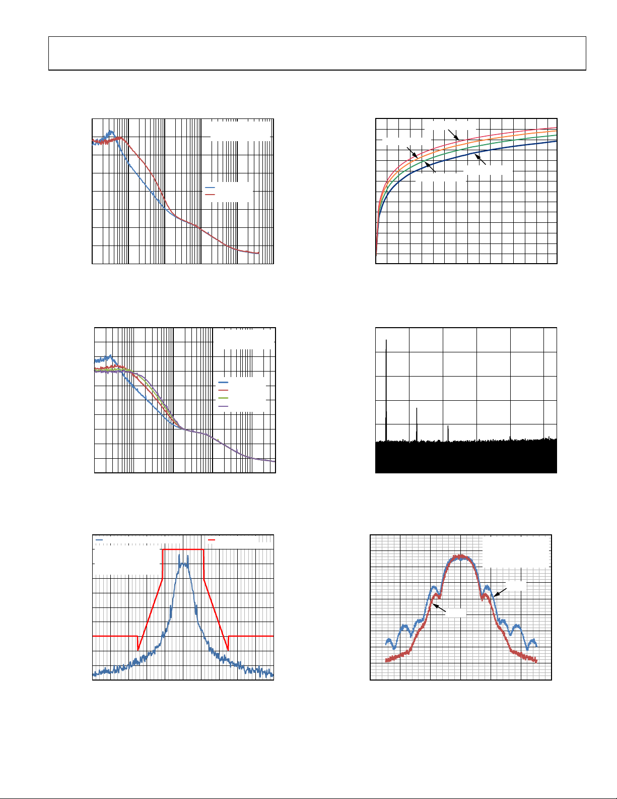
TYPICAL PERFORMANCE CHARACTERISTICS
80
–90
–100
–110
–120
–130
PHASE NOISE (dBc/Hz)
–140
–150
–160
1 10 100 1k 10k 100k
FREQUENCY OFFSET (kHz)
RF FREQ = 460MHz
TCXO = 19.2MHz
ICP= 0.3mA
= 0.9mA
I
CP
Figure 11. Phase Noise Response at 460 MHz, VDD = 3 V
08635-077
16
12
8
PA_BIAS = 9µA
4
0
–4
–8
–12
–16
–20
–24
RF OUTPUT POWER (dBm)
–28
–32
–36
–40
0 4 8 12 16 20 24 28 32 36 40 44 48 52 56 60
PA_BIAS = 11µA
PA_BIAS = 7µA
PA SETTING
PA_BIAS = 5µA
Figure 14. RF Output Power vs. PA Setting
08635-012
60
–70
–80
–90
–100
–110
–120
–130
PHASE NOISE (dBc/Hz)
–140
–150
–160
1 10 100 1k 10k
FREQUENCY OFFSET (kHz)
RF FREQ = 8 68M Hz
TCXO = 19. 2 M Hz
ICP= 0.3mA
I
= 0.9mA
CP
I
= 1.5mA
CP
I
= 2.1mA
CP
Figure 12. Phase Noise Response at 868 MHz, VDD = 2.3 V
20
DEMODULATI O N = G F SK
10
DATA RATE = 2.4kbps
f
= 1.2kHz
DEV
RF FREQ = 4 70M Hz
0
IFBW = 4kHz
–10
–20
–30
–40
–50
OUTPUT POWER (dBm)
–60
–70
–80
–25,000
0
–20,000
–15,000
FREQUENCY OFFSET FROM CARRIER (Hz)
–5000
–10,000
FCC PART 90
EMISSION MASK D
5000
10,000
15,000
Figure 13. Output Spectrum in FCC Part 90 Emission Mask D
and GFSK Modes
20,000
25,000
20
0
–20
–40
–60
OUTPUT POWER (dBm)
–80
–100
300 800 1300 1800 2300 2800
08635-078
FREQUENCY (MHz)
08635-013
Figure 15. PA Output Harmonic Response with T-Stage LC Filter
10
0
–10
–20
–30
–40
–50
OUTPUT POWER (dBm)
–60
–70
–80
867.97 867.98 867.99 868.00 868.01 868.02 868.03
08635-079
GFSK
FREQUENCY (MHz)
DATA RATE = 9.6kbps
DATA = P RBS9
f
= 2.4kHz
DEV
RF FREQ = 868MHz
2FSK
08635-014
Figure 16. Output Spectrum in 2FSK and GFSK Modes
Rev. 0 | Page 17 of 60
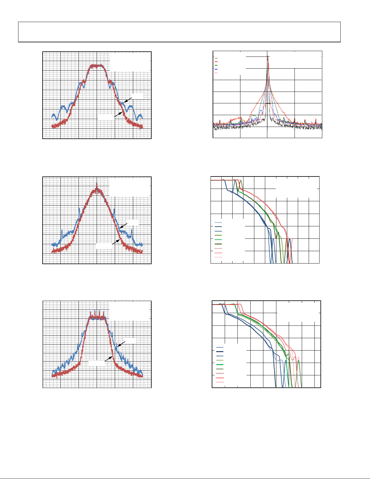
ADF7021-V
R
R
10
0
–10
–20
–30
–40
–50
OUTPUT POWER (dBm)
–60
–70
–80
867.97 867.98 867.99 868.00 868.01 868.02 868.03
FREQUENCY (MHz)
DATA RATE = 9.6kbps
DATA = P RBS 9
f
= 2.4kHz
DEV
RF FREQ = 86 8M Hz
RC2FSK
2FSK
Figure 17. Output Spectrum in 2FSK and Raised Cosine 2FSK Modes
08635-015
RAMP RATE:
10
CW ONLY
256 CODES/BI T
128 CODES/BI T
0
64 CODES/BIT
32 CODES/BIT
–10
–20
–30
OUTPUT PO WER (dBm)
–40
–50
–60
–100 –50 500 100
FREQUENCY OFFSET (kHz)
TRACE = MAX HOLD
PA ON/OFF RATE = 3Hz
PA ON/OFF CYCLES = 10,000
V
= 3.0V
DD
Figure 20. Output Spectrum in Maximum Hold
for Various PA Ramp Rate Options
08635-018
10
0
–10
–20
–30
–40
–50
OUTPUT POWER (dBm)
–60
–70
–80
867.97 867.98 867.99 868.00 868.01 868.02 868.03
FREQUENCY (MHz)
DATA RATE = 9.6kbps
DATA = PRBS9
f
DEV
RF FREQ = 868M Hz
RC3FSK
= 2.4kHz
3FSK
Figure 18. Output Spectrum in 3FSK and Raised Cosine 3FSK Modes
10
0
–10
–20
–30
–40
–50
–60
OUTPUT PO WER (dBm)
–70
–80
–90
867.94 867.96 867.98 868.00 868.02 868.04 868.06
RC4FSK
FREQUENCY (MHz)
DATA RATE = 9.6kbps
DATA = PRBS9
f
= 2.4kHz
DEV
RF FREQ = 868M Hz
4FSK
Figure 19. Output Spectrum in 4FSK and Raised Cosine 4FSK Modes
0
–1
–2
–3
–40°C, 2.3V
–4
LOG BE
08635-016
–40°C, 3V
–40°C, 3.6V
+25°C, 2. 3V
–5
+25°C, 3V
+25°C, 3. 6V
+85°C, 2. 3V
–6
+85°C, 3V
+85°C, 3. 6V
–7
–125 –123 –121 –119 –117 –115 –113 –111 –109 –107 –105
RF INPUT POWER (dBm)
DATA RAT E = 2.4kbps
f
= 4.8Hz
DEV
RF FREQ = 868M Hz
IFBW = 9kHz
08635-019
Figure 21. 2FSK Sensitivity vs. VDD and Temperature at 868 MHz
0
–1
–2
–3
–40°C, 2.3V
–4
LOG BE
08635-017
–40°C, 3V
–40°C, 3.6V
+25°C, 2.3V
–5
+25°C, 3V
+25°C, 3.6V
+85°C, 2.3V
–6
+85°C, 3V
+85°C, 3.6V
–7
–127 –125 –123 –121 –119 –117 –115 –113 –111
RF INPUT POWER (dBm)
DATA RATE = 1.2kbps
f
= 2.4Hz
DEV
RF FREQ = 46 0M Hz
IFBW = 9kHz
08635-020
Figure 22. 2FSK Sensitivity vs. VDD and Temperature at 460 MHz
Rev. 0 | Page 18 of 60

ADF7021-V
–
0.6
0.5
0.4
0.3
BIT ERROR RATE
0.2
DATA RATE = 1.2kbps
f
= 2.4Hz
DEV
RF FREQ = 8 68M Hz
IFBW = 9kHz
–40°C, 2.3V
–40°C, 3V
–40°C, 3.6V
+25°C, 2.3V
+25°C, 3V
+25°C, 3.6V
+85°C, 2.3V
+85°C, 3V
+85°C, 3.6V
RSSI LEVEL (dBm)
–40
–60
–80
–100
20
RSSI
READBACK LEVEL
ACTUAL RF INPUT LEVEL
0.1
0
–130 –125 –120 –115 –110 –105
RF INPUT PO WER (dBm)
Figure 23. 2FSK Sensitivity vs. VDD and Temperature at 868 MHz
0.6
0.5
0.4
0.3
BIT ERROR RATE
0.2
0.1
0
–130 –125 –120 –115 –110 –105
RF INPUT PO WER (dBm)
Figure 24. 2FSK Sensitivity vs. V
DATA RATE = 1.2kbps
f
= 2.4Hz
DEV
RF FREQ = 460M Hz
IFBW = 9kHz
–40°C, 2.3V
–40°C, 3V
–40°C, 3.6V
+25°C, 2.3V
+25°C, 3V
+25°C, 3.6V
+85°C, 2.3V
+85°C, 3V
+85°C, 3.6V
and Temperature at 460 MHz
DD
–120
–140
–122.5 –112.5 –102.5 –92.5 –82.5 –72.5 –62.5 –52.5 –42.5
08635-021
RF INPUT POWER (dBm)
08635-023
Figure 26. Digital RSSI Readback Linearity
80
70
60
50
40
30
BLOCKING (dB)
20
459.70
CALIBRATED
UNCALIBRATED
459.75
459.80
459.85
BLOCKER FREQ UE NCY ( M Hz)
459.90
459.95
460.00
460.05
460.10
460.15
08635-080
10
0
–10
08635-022
Figure 27. Image Rejection, Uncalibrated vs. Calibrated
100
90
80
70
60
50
40
30
BLOCKING (dB )
20
10
0
–10
–20 –15 –10 –5 0 5 10 15 20
FREQUENCY OF F SE T (M Hz)
08635-024
Figure 25. Wideband Interference Rejection (Modulated Carrier Is Swept 20 MHz
Either Side of an 868 MHz Modulated GFSK 2.4 kHz/4.8 kbps Wanted Signal at the
Sensitivity Point (−106.5 dBm); the Power Level of the Blocker Is Adjusted to
Give a BER of 10
−2
; Interferer Is a GFSK PRBS15 4.8 kHz/2.4 kHz Signal)
2.5
0
+90°C
–2.5
–5.0
–7.5
–10.0
–12.5
–15.0
–17.5
–20.0
–22.5
ATTENUATION (dB)
–25.0
–27.5
–30.0
–32.5
–35.0
–37.5
90 92 94 96 98 100 102 104 106 108 110
–40°C
IF FREQUENCY (kHz)
08635-025
Figure 28. Variation of IF Filter Response with Temperature
(IF_FILTER_BW = 9 kHz, Temperature Range Is −40°C to +90°C in 10° Steps)
Rev. 0 | Page 19 of 60

ADF7021-V
–
–
100
–102
–104
–106
–108
–110
–112
SENSITIVITY POINT (dBm)
–114
–116
DISCRIMINAT OR BANDWIDTH =
1× FSK FREQUENCY DEVIATI ON
–118
0 0.2 0.4 0.6 0.8 1.0 1.2
DISCRIMINAT OR BANDWIDTH =
2× FSK FREQUE NC Y D EVIAT ION
MODULATION INDEX
RF FREQ = 860MHz
2FSK MODULATION
DATA RATE = 9.6kbps
IFBW = 25kHz
= 3.0V
V
DD
TEMPERATURE = 25 ° C
Figure 29. 2FSK Sensitivity vs. Modulation Index and Correlator
Discriminator Bandwidth
0
–1
–2
VITERBI DE T ECTION
–3
THRESHOLD DET ECTION
70
MIXER
3, 72
HIGH MIXER
LINEARITY
(MEDIUM GAIN MODE)
LNA GAIN, FILTER GAIN
–80
IP3 = –5dBm
–90
–100
IP3 = –3dBm
–110
SENSITIVITY (dBm)
–120
–130
08635-026
DEFAULT
LINEARITY
(LOW GAIN MODE)
2FSK MODULATION
DATA RATE = 9.6kb ps
f
DEV
IFBW = 12.5kHz
DEMOD = CORREL ATOR
SENSITIVITY @ BER = 10
IP3 = –9dBm
IP3 = –13.5dBm
10, 72
= 4kHz
IP3 = –20dBm
(HIGH GAIN MODE)
–3
IP3 = –24dBm
30, 72
08635-028
Figure 31. 2FSK Receiver Sensitivity vs. LNA Gain/IF Filter Gain and Mixer
Linearity Settings (Input IP3 at Each Setting Also Shown)
–4
LOG BER
–5
3FSK MODULATION
V
= 3.0V, T EMP = 25°C
DD
DATA RATE = 9.6kbps
–6
f
= 2.4kHz
DEV
RF FREQ = 868MHz
IFBW = 18.75kHz
–7
–120 –118 –116 –114 –112 –110 –108 –106 –104 –102 –100
INPUT POWER (dBm)
Figure 30. 3FSK Receiver Sensitivity Using Viterbi Detection and
Threshold Detection
08635-027
Rev. 0 | Page 20 of 60

ADF7021-V
V
FREQUENCY SYNTHESIZER
REFERENCE INPUT
The on-board crystal oscillator circuitry (see Figure 32) can use
a quartz crystal as the PLL reference. A quartz crystal with a frequency tolerance of ≤10 ppm for narrow-band applications is
recommended. It is possible to use a quartz crystal with >10 ppm
tolerance, but compensation for the frequency error of the crystal
is necessary to comply with the absolute frequency error specifications of narrow-band regulations (for example, ARIB STD-T67
and ETSI EN 300 220).
The oscillator circuit is enabled by setting Bit DB12 in Register 1
high. It is enabled by default on power-up and is disabled by
bringing CE low. Errors in the crystal can be corrected using
the automatic frequency control (AFC) feature or by adjusting
the fractional-N value (see the N Counter section).
OSC1
Figure 32. Crystal Oscillator Circuit on the ADF7021-V
Two parallel resonant capacitors are required for oscillation at
the correct frequency. Their values are dependent on the crystal
specification. The resonant capacitors should be selected to
ensure that the series value of capacitance added to the PCB
track capacitance adds up to the specified load capacitance of
the crystal, usually 12 pF to 20 pF. Track capacitance values vary
from 2 pF to 5 pF, depending on board layout. When possible,
choose capacitors that have a very low temperature coefficient
to ensure stable frequency operation over all conditions.
Using a TCXO Reference
A single-ended reference (TCXO, VCXO, or OCXO) can also be
used with the ADF7021-V. This is recommended for applications
that have absolute frequency accuracy requirements of <10 ppm,
such as applications requiring compliance with ARIB STD-T67
or ETSI EN 300 220. The following are two options for interfacing the ADF7021-V to an external reference oscillator.
• An oscillator with CMOS output levels can be applied to
OSC2. The internal oscillator circuit should be disabled by
setting Bit DB12 in Register 1 low.
• An oscillator with 0.8 V p-p levels can be ac-coupled through
a 22 pF capacitor into OSC1. The internal oscillator circuit
should be enabled by setting Bit DB12 in Register 1 high.
Programmable Crystal Bias Current
Bias current in the oscillator circuit can be configured from
20 µA to 35 µA by writing to the XTAL_BIAS bits (Register 1,
Bits[DB14:DB13]). Increasing the bias current allows the crystal
oscillator to power up faster.
OSC2
CP1CP2
08635-030
CLKOUT Divider and Buffer
The CLKOUT circuit takes the reference clock signal from the
oscillator section, shown in Figure 32, and supplies a divideddown, 50:50 mark/space signal to the CLKOUT pin. The
CLKOUT signal is inverted with respect to the reference clock.
An even divide from 2 to 30 is available; this divide number is
set in Register 1, Bits[DB10:DB7]. On power-up, the CLKOUT
defaults to divide-by-8.
DD
CLKOUT
ENABLE BIT
DIVIDER
1TO 15
Figure 33. CLKOUT Stage
÷2
CLKOUTOSC1
08635-031
To disable CLKOUT, set the divide number to 0. The output
buffer can drive a load of up to 20 pF with a 10% rise time at
4.8 MHz. Faster edges can result in some spurious feedthrough
to the output. A series resistor (1 kΩ) can be used to slow the
clock edges to reduce these spurs at the CLKOUT frequency.
R Counter
The 3-bit R counter divides the reference input frequency by an
integer from 1 to 7. The divided-down signal is presented as the
reference clock to the phase frequency detector (PFD). The
divide ratio is set in Register 1, Bits[DB6:DB4]. Maximizing the
PFD frequency reduces the N value. This reduces the noise multiplied at a rate of 20 log(N) to the output and reduces occurrences
of spurious components.
Register 1 defaults to R = 1 on power-up.
PFD (Hz) = XTAL/R
Loop Filter
The loop filter integrates the current pulses from the charge
pump to form a voltage that tunes the output of the VCO to the
desired frequency. It also attenuates spurious levels generated by
the PLL. A typical loop filter design is shown in Figure 34.
CHARGE
PUMP OUT
Figure 34. Typical Loop Filter Configuration
VCO
08635-032
The loop should be designed so that the loop bandwidth (LBW) is
approximately 6 kHz. This provides a good compromise between
in-band phase noise and out-of-band spurious rejection. Widening
the LBW excessively reduces the time spent jumping between
frequencies, but it can cause insufficient spurious attenuation.
The loop filter design on the EVAL-ADF7021-VDBxZ should
be used for optimum performance.
Rev. 0 | Page 21 of 60

ADF7021-V
V
The free design tool ADIsimSRD™ Design Studio can also be
used to design loop filters for the ADF7021-V. See the ADIsimSRD
Design Studio website (www.analog.com/adisimsrd) for details).
N Counter
The feedback divider in the ADF7021-V PLL consists of an
8-bit integer counter (set using Register 0, Bits[DB26:DB19])
and a 15-bit, Σ- fractional-N divider (set using Register 0,
Bits[DB18:DB4]). The integer counter is the standard pulseswallow type that is common in PLLs. It sets the minimum
integer divide value to 23. The fractional divide value provides
very fine resolution at the output, where the output frequency
of the PLL is calculated as
__NFRACTIONAL
f
OUT
XTAL
R
⎛
⎜
⎜
⎝
NINTEGER
+×=
15
2
⎞
⎟
⎟
⎠
When RF_DIVIDE_BY_2 is enabled (see the Vo lt ag e
Controlled Oscillator (VCO) section), this formula becomes
_
f
OUT
XTAL
R
0.5
⎛
INTEGER_N
⎜
⎝
+××=
2
NFRACTIONAL
15
The combination of INTEGER_N (maximum = 255) and
FRACTIONAL_N (maximum = 32,768/32,768) gives a
maximum N divider of 255 + 1. Therefore, the minimum
usable PFD is
PFD
MIN
(Hz)+=
FrequencyOutputRequiredMaximum
()
1255
⎞
⎟
⎠
The serial interface operates from a regulator supply. Therefore,
to write to the part, CE must be high and the regulator voltage
must be stabilized. Regulator status (CREG4) can be monitored
using the REGULATOR_READY signal from the MUXOUT pin.
MUXOUT
The MUXOUT pin allows access to various digital points in the
ADF7021-V. The state of MUXOUT is controlled in Register 0,
Bits[DB31:DB29].
REGULATOR_READY
REGULATOR_READY is the default setting on MUXOUT after
the transceiver is powered up. The power-up time of the regulator
is typically 50 µs. Because the serial interface is powered from
the regulator, the regulator must be at its nominal voltage before
the ADF7021-V can be programmed. The regulator status can
be monitored at MUXOUT. When the regulator ready signal on
MUXOUT is high, programming of the ADF7021-V can begin.
DD
REGULATOR_RE ADY ( DE FAULT)
FILTER_CAL_COMPLETE
DIGITAL_LOCK_DETECT
RSSI_READY
Tx_Rx
LOGIC_ZERO
TRISTATE
LOGIC_ONE
MUX CONTROL
MUXOUT
For example, when operating in the European 868 MHz to
870 MHz band, PFD
REFERE NC E IN
÷R
= 3.4 MHz.
MIN
PFD/
CHARGE
PUMP
THIRD-ORDER
Σ-Δ MODULATOR
Figure 35. Fractional-N PLL
VCO
÷N
INTEGER_NFRACTIONAL_N
08635-033
Voltage Regulators
The ADF7021-V contains four regulators to supply stable
voltages to the part. The nominal regulator voltage is 2.3 V.
Regulator 1 requires a 3.9 resistor and a 100 nF capacitor in
series between CREG1 and ground, whereas the other regulators require a 100 nF capacitor connected between CREGx and
ground. When CE is high, the regulators and other associated
circuitry are powered on, drawing a total supply current of
2 mA. Bringing the CE pin low disables the regulators, reduces
the supply current to less than 1 µA, and erases all values held
in the registers.
GND
Figure 36. MUXOUT Circuit
FILTER_CAL_COMPLETE
MUXOUT can be set to FILTER_CAL_COMPLETE. This signal
goes low for the duration of both a coarse IF filter calibration
and a fine IF filter calibration. It can be used as an interrupt to
a microcontroller to signal the end of the IF filter calibration.
DIGITAL_LOCK_DETECT
DIGITAL_LOCK_DETECT indicates when the PLL has locked.
The lock detect circuit is located at the PFD. When the phase
error on five consecutive cycles is less than 15 ns, lock detect is
set high. Lock detect remains high until a 25 ns phase error is
detected at the PFD.
RSSI_READY
MUXOUT can be set to RSSI_READY. This indicates that the
internal analog RSSI has settled and that a digital RSSI readback
can be performed.
Tx_Rx
Tx_Rx signifies whether the ADF7021-V is in transmit or
receive mode. When in transmit mode, this signal is low.
When in receive mode, this signal is high. It can be used to
control an external Tx/Rx switch.
08635-034
Rev. 0 | Page 22 of 60

ADF7021-V
VOLTAGE CONTROLLED OSCILLATOR (VCO)
To minimize feedthrough and spurious emissions, the external
VCO must be chosen to operate at a minimum of twice the
required RF frequency. The VCO frequency is divided by 2 inside
the synthesizer loop, providing the required frequency for the
transmitter and for the local oscillator (LO) of the receiver. For
improved phase noise performance, an additional divide-by-2
can be enabled by setting the RF_DIVIDE_BY_2 bit (Bit DB18)
in Register 1.
As an example, for 80 MHz operation, a 160 MHz external VCO
could be used with the RF_DIVIDE_BY_2 bit disabled, or a
320 MHz VCO could be used with the RF_DIVIDE_BY_2 bit
enabled to support operation in the 80 MHz band. Assuming
that both VCOs have similar phase noise performance, the
320 MHz design using the additional divide-by-2 should result
in improved transmit ACP, as well as improved ACR, blocking,
and image rejection in the receiver.
The maximum VCO frequency of operation supported on the
ADF7021-V is 1920 MHz, which results in a maximum RF
channel frequency of 960 MHz using a 2× VCO or 480 MHz
using a 4× VCO.
EXTERNAL
COMPONENTS
REF
TCXO/XTAL
LOOP
FILTER
÷R
PFD/CP
ADF7021-V
Figure 37. Voltage Controlled Oscillator (VCO)
VCO
÷2
÷N
SYNTH
FREQUENCY
MUX
TO
÷2
PA
08635-036
The VCO tuning voltage can be checked for a particular RF
output frequency by measuring the voltage on the CPOUT pin
when the part is fully powered up in transmit or receive mode.
The VCO tuning range of the external VCO must be 0.2 V to 2 V.
The input impedance of the L2 pin is programmable and can
be selected to have a high impedance value or 50 Ω impedance,
depending on the VCO selected. The impedance of this pin can
be set using the BUFFER_IMPEDANCE bit (Bit DB17) in
Register 1.
CHOOSING A VCO FOR BEST SYSTEM PERFORMANCE
The interaction between the RF VCO frequency and the reference frequency can lead to fractional spur creation. When the
synthesizer is in fractional mode (that is, the RF VCO and
reference frequencies are not integer related), spurs can appear
on the VCO output spectrum at an offset frequency that
corresponds to the difference frequency between an integer
multiple of the reference and the VCO frequency.
These spurs are attenuated by the loop filter. They are more
noticeable on channels close to integer multiples of the reference
where the difference frequency may be inside the loop bandwidth
(thus, the name integer boundary spurs). The occurrence of
these spurs is rare because the integer frequencies are around
multiples of the reference, which is typically >10 MHz. To avoid
having very small or very large values in the fractional register,
choose a suitable reference frequency.
In addition to spurious considerations, the selection of a high
performance VCO with very low phase noise is essential to
minimize the ACP performance of the transmitter and to
maximize the ACR and blocking resilience of the receiver.
Rev. 0 | Page 23 of 60

ADF7021-V
3
6
TRANSMITTER
RF OUTPUT STAGE
The power amplifier (PA) of the ADF7021-V is based on a
single-ended, controlled current, open-drain amplifier that has
been designed to deliver up to 13 dBm into a 50 Ω load at a
maximum frequency of 960 MHz.
The PA output current and, consequently, the output power
are programmable over a wide range. The PA configuration is
shown in Figure 38. The output power is set using Register 2,
Bits[DB18:DB13].
REGISTER 2,
BITS[DB12:DB11]
2
6
IDAC
RFOUT
+
RFGND
FROM VCO
Figure 38. PA Configuration
The PA is equipped with overvoltage protection, which makes it
robust in severe mismatch conditions. Depending on the application, users can design a matching network for the PA to exhibit
optimum efficiency at the desired radiated output power level for
a wide range of antennas, such as loop or monopole antennas.
See the LNA/PA Matching section for more information.
PA Ramping
When the PA is switched on or off quickly, its changing input
impedance momentarily disturbs the VCO output frequency.
This process is called VCO pulling, and it manifests as spectral
splatter or spurs in the output spectrum around the desired
carrier frequency. Some radio emissions regulations place
limits on these PA transient-induced spurs (for example, the
ETSI EN 300 220 regulations). By gradually ramping the PA
on and off, PA transient spurs are minimized.
The ADF7021-V has built-in PA ramping configurability. As
Figure 39 illustrates, there are eight ramp rate settings, defined
as a certain number of PA setting codes per one data bit period.
The PA steps through each of its 64 code levels but at different
speeds for each setting. The ramp rate is set by configuring
Bits[DB10:DB8] in Register 2.
If the PA is enabled/disabled by the PA_ENABLE bit (Register 2,
Bit DB7), it ramps up and down. If it is enabled/disabled by the
Tx/Rx bit (Register 0, Bit DB27), it ramps up and turns hard off.
REGISTER 2,
BITS[DB18:DB13]
REGISTER 2, BIT DB7
REGISTE R 0, BIT DB27
08635-037
DATA BITS
PA RAMP 0
(NO RAMP)
PA RAMP 1
(256 CODES PER BI T)
PA RAMP 2
(128 CODES PER BI T)
PA RAMP 3
(64 CODES PER BIT)
PA RAMP 4
(32 CODES PER BIT)
PA RAMP 5
(16 CODES PER BIT)
PA RAMP 6
(8 CODES PER BIT)
PA RAMP 7
(4 CODES PER BIT)
1 2
4 ... 8 ... 1
08635-038
Figure 39. PA Ramping Settings
PA Bias Currents
The PA_BIAS bits (Register 2, Bits[DB12:DB11]) facilitate an
adjustment of the PA bias current to further extend the output
power control range, if necessary. If this feature is not required,
the default value of 9 µA is recommended. If output power
greater than 10 dBm is required, a PA bias setting of 11 µA is
recommended. The output stage is powered down by resetting
Register 2, Bit DB7 to 0.
MODULATION SCHEMES
The ADF7021-V supports 2FSK, 3FSK, and 4FSK modulation.
The implementation of these modulation schemes is shown in
Figure 40.
REF
Tx_FREQUENCY_
DEVIATION
GAUSSIAN
OR
RAISED COSINE
FILTERING
MUX
LOOP FILTER
THIRD-ORDER
Σ-Δ MODULATOR
2FSK
3FSK
1 – D2 PR
SHAPING
4FSK
4FSK
BIT SYMBO L
MAPPER
VCO
÷N
INTEGER_N
PRE-
CODER
PFD/
CHARGE
PUMP
FRACTIONAL_N
Figure 40. Transmit Modulation Implementation
÷2
TO
PA STAGE
TxRxDATA
08635-039
Rev. 0 | Page 24 of 60

ADF7021-V
N
I
N
N
I
N
Setting the Transmit Data Rate
In all modulation modes except for oversampled 2FSK mode, an
accurate clock is provided on the TxRxCLK pin to latch the data
from the microcontroller into the transmit section at the required
data rate. The exact frequency of this clock is defined by
=
CLKDATA
XTAL
32××
VIDECDR_CLK_DIDIVIDEDEMOD_CLK_
where:
XTAL is the crystal or TCXO frequency.
DEMOD_CLK_DIVIDE is the divider that sets the demodulator
clock rate (Register 3, Bits[DB9:DB6]).
CDR_CLK_DIVIDE is the divider that sets the CDR clock rate
(Register 3, Bits[DB17:DB10]).
See the Register 3—Transmit/Receive Clock Register section for
more programming information.
Setting the FSK Transmit Deviation Frequency
In all modulation modes, the deviation from the center
frequency is set using the Tx_FREQUENCY_DEVIATION
bits (Register 2, Bits[DB27:DB19]).
The deviation from the center frequency in Hz is as follows:
For direct RF output,
DEV
Tx_FREQUE
PFD
f
(Hz)
×
=
CY_DEVIAT
16
2
O
With RF_DIVIDE_BY_2 (Register 1, Bit DB18) enabled,
DEV
Tx_FREQUE
PFD
f
5.0(Hz)
×
×=
CY_DEVIAT
16
2
O
where Tx_FREQUENCY_DEVIATION is a number from 1 to
511 (Register 2, Bits[DB27:DB19]).
In 4FSK modulation, the four symbols (00, 01, 11, 10) are
transmitted as ±3 × f
and ±1 × f
DEV
DEV
.
Binary Frequency Shift Keying (2FSK)
Binary frequency shift keying is implemented by setting the
N value for the center frequency and then toggling it with the
TxRxDATA line. The deviation from the center frequency is set
using the Tx_FREQUENCY_DEVIATION bits (Register 2,
Bits[DB27:DB19]).
2FSK is selected by setting the MODULATION_SCHEME bits
(Register 2, Bits[DB6:DB4]) to 000.
Minimum shift keying (MSK) or Gaussian minimum shift
keying (GMSK) is supported by selecting 2FSK modulation
and using a modulation index of 0.5. A modulation index of 0.5
is set by configuring Register 2, Bits[DB27:DB19] for an
= 0.25 × transmit data rate.
f
DEV
Three-Level Frequency Shift Keying (3FSK)
In three-level FSK modulation—3FSK, also known as modified
duobinary FSK and as partial response maximum likelihood
Class 4 (PRML4) signaling—the binary data (Logic 0 and Logic 1)
is mapped onto three distinct frequencies: the carrier frequency
), the carrier frequency minus a deviation frequency (fC − f
(f
C
and the carrier frequency plus the deviation frequency (f
C
+ f
DEV
DEV
).
A Logic 0 is mapped to the carrier frequency, whereas a Logic 1
is mapped onto either the f
frequency or the fC + f
C
DEV
DEV
− f
frequency.
0
–1
f
–
f
C
DEV
RF FREQUENCY
Figure 41. 3FSK Symbol-to-Frequency Mapping
+1
f
f
+
f
C
C
DEV
08635-040
Compared with 2FSK, this bit-to-frequency mapping results
in a reduced transmission bandwidth because some energy is
removed from the RF sidebands and transferred to the carrier
frequency. At low modulation index, 3FSK improves the transmit spectral efficiency by up to 25% when compared with 2FSK.
The bit-to-symbol mapping for 3FSK is implemented using a
linear convolutional encoder that also permits Viterbi detection
to be used in the receiver. A block diagram of the transmit hardware used to realize this system is shown in Figure 42. The
convolutional encoder polynomial used to implement the
transmit spectral shaping is
2
P(D) = 1 − D
where:
P is the convolutional encoder polynomial.
D is the unit delay operator.
A digital precoder with transfer function 1/P(D) implements
2
an inverse modulo-2 operation of the 1 − D
shaping filter in
the transmitter.
Tx DATA
0, 1
PRECODER
1/P(D)
0, 1
CONVOLUTIONAL
ENCODER
P(D)
0, +1, –1
FSK MOD
CONTROL
AND
DATA FILTERING
Figure 42. 3FSK Encoding
f
C
f
+
f
C
DEV
f
–
f
C
DEV
TO
N DIVIDER
),
08635-041
Rev. 0 | Page 25 of 60

ADF7021-V
The signal mapping of the input binary transmit data to the
three-level convolutional output is shown in Tab l e 9 . The
convolutional encoder restricts the maximum number of
sequential +1s or −1s to two and delivers an equal number of
+1s and −1s to the FSK modulator, thus ensuring equal spectral
energy in both RF sidebands.
Table 9. Three-Level Signal Mapping of the Convolutional
Encoder
TxDATA
Precoder
1 0 1 1 0 0 1 0 0 1
1 0 0 1 0 1 1 1 1 0
Output
Encoder
+1 0 −1 +1 0 0 +1 0 0 −1
Output
Another property of this encoding scheme is that the transmitted symbol sequence is dc-free, which facilitates symbol
detection and frequency measurement in the receiver. In
addition, no code rate loss is associated with this three-level
convolutional encoder; that is, the transmitted symbol rate is
equal to the data rate presented at the transmit data input.
3FSK is selected by setting the MODULATION_SCHEME bits
(Register 2, Bits[DB6:DB4]) to 010. It can also be used with
raised cosine filtering to further increase the spectral efficiency
of the transmit signal.
Four-Level Frequency Shift Keying (4FSK)
In 4FSK modulation, two bits per symbol spectral efficiency is
realized by mapping consecutive input bit-pairs in the Tx data
bit stream to one of four possible symbols (−3, −1, +1, +3). Thus,
the transmitted symbol rate is half the input bit rate. These
symbols are mapped to equally spaced discrete frequencies
centered on the RF carrier at
, −1f
, +1f
−3f
where f
DEV
DEV
is programmed using the Tx_FREQUENCY_
DEV
, and +3f
DEV
DEV
DEVIATION bits (Bits[DB27:DB19] in Register 2) and is also
equal to half the frequency spacing between adjacent symbols.
By minimizing the separation between symbol frequencies,
4FSK can have high spectral efficiency. The bit-to-symbol
mapping for 4FSK is gray coded and is shown in Figure 43.
SYMBOL
FREQUENCIES
Tx DATA
+3f
+f
–f
–3f
Figure 43. 4FSK Bit-to-Symbol Mapping
00011011
f
DEV
DEV
DEV
DEV
t
08635-042
The inner deviation frequencies (+f
DEV
and −f
) are set using
DEV
the Tx_FREQUENCY_DEVIATION bits (Bits[DB27:DB19] in
Register 2). The outer deviation frequencies are automatically
set to three times the inner deviation frequency.
The transmit clock from Pin TxRxCLK is available after writing
to Register 3 in the power-up sequence for receive mode. The
MSB of the first symbol should be clocked into the ADF7021-V
on the first transmit clock pulse from the ADF7021-V after
writing to Register 3. See Figure 6 and Figure 7 for more timing
information; see Figure 54 and Figure 55 for the power-up
sequences.
Oversampled 2FSK
In oversampled 2FSK, there is no data clock from the TxRxCLK
pin. Instead, the transmit data at the TxRxDATA pin is sampled
at 32 times the programmed rate.
Oversampled 2FSK is the only modulation mode that can be
used with the UART mode interface for data transmission (see
the Interfacing to a Microcontroller/DSP section for more
information).
SPECTRAL SHAPING
Gaussian or raised cosine filtering can be used to improve
transmit spectral efficiency. The ADF7021-V supports Gaussian
filtering (bandwidth time [BT] = 0.5) on 2FSK modulation.
Raised cosine filtering can be used with 2FSK, 3FSK, or 4FSK
modulation. The roll-off factor (alpha) of the raised cosine filter
has programmable options of 0.5 and 0.7. Both the Gaussian
and raised cosine filters are implemented using linear phase
digital filter architectures that deliver precise control over the
BT and alpha filter parameters, and guarantee a transmit spectrum
that is very stable over temperature and supply variation.
Gaussian Frequency Shift Keying (GFSK)
Gaussian frequency shift keying reduces the bandwidth occupied
by the transmitted spectrum by digitally prefiltering the transmit
data. The BT product of the Gaussian filter used is 0.5.
Gaussian filtering can be used only with 2FSK modulation. GFSK
is selected by setting Register 2, Bits[DB6:DB4] to 001.
Raised Cosine Filtering
Raised cosine filtering provides digital prefiltering of the transmit
data by using a raised cosine filter with a roll-off factor (alpha)
of either 0.5 or 0.7. The alpha is set to 0.5 by default, but the
raised cosine filter bandwidth can be increased to provide less
aggressive data filtering by using an alpha of 0.7 (set Register 2,
Bit DB30 to Logic 1). Raised cosine filtering can be used with
2FSK, 3FSK, and 4FSK modulation.
Raised cosine filtering is enabled by setting Register 2,
Bits[DB6:DB4] as shown in Tab le 1 0.
Rev. 0 | Page 26 of 60

ADF7021-V
MODULATION AND FILTERING OPTIONS
The various modulation and data filtering options for the
ADF7021-V are described in Tabl e 10 .
Table 10. Modulation and Filtering Options
Register 2,
Modulation Data Filtering
Bits[DB6:DB4]
Binary FSK
2FSK None 000
MSK1 None 000
OQPSK with Half Sine
Baseband Shaping
None 000
2
GFSK Gaussian 001
GMSK3 Gaussian 001
RC2FSK Raised cosine 101
Oversampled 2FSK None 100
Three-Level FSK
3FSK None 010
RC3FSK Raised cosine 110
Four-Level FSK
4FSK None 011
RC4FSK Raised cosine 111
1
MSK is 2FSK modulation with a modulation index = 0.5.
2
Offset quadrature phase shift keying (OQPSK) with half sine baseband
shaping is spectrally equivalent to MSK.
3
GMSK is GFSK with a modulation index = 0.5.
TRANSMIT LATENCY
Transmit latency is the delay time from the sampling of a
bit/symbol by the TxRxCLK signal to when that bit/symbol
appears at the RF output. The latency without any data filtering
is 1 bit. The addition of data filtering adds a further latency as
indicated in Tab l e 1 1 .
It is important that the ADF7021-V be left in transmit mode
after the last data bit is sampled by the data clock to account for
this latency. The ADF7021-V should stay in transmit mode for
a time equal to the number of latency bit periods for the applied
modulation scheme. This ensures that all of the data sampled by
the TxRxCLK signal appears at RF.
The figures for latency in Tab l e 1 1 assume that the positive
TxRxCLK edge is used to sample data (default). If the TxRxCLK
is inverted by setting Register 2, Bits[DB29:DB28], an additional
0.5 bit latency can be added to all values in Ta b le 1 1.
Table 11. Bit/Symbol Latency in Transmit Mode for Various
Modulation Schemes
Modulation Latency
2FSK 1 bit
GFSK 4 bits
RC2FSK, alpha = 0.5 5 bits
RC2FSK, alpha = 0.7 4 bits
3FSK 1 bit
RC3FSK, alpha = 0.5 5 bits
RC3FSK, alpha = 0.7 4 bits
4FSK 1 symbol
RC4FSK, alpha = 0.5 5 symbols
RC4FSK, alpha = 0.7 4 symbols
TEST PATTERN GENERATOR
The ADF7021-V has a number of built-in test pattern generators
that can be used to facilitate radio link setup or RF measurement.
A full list of the supported test patterns is shown in Tabl e 12 .
The data rate for these test patterns is the programmed data rate
set in Register 3.
The PN9 sequence is suitable for test modulation when carrying
out adjacent channel power (ACP) or occupied bandwidth
measurements.
Table 12. Transmit Test Pattern Generator Options
Register 15,
Test Pattern
Normal 000
Transmit carrier only 001
Transmit +f
Transmit −f
tone only 010
DEV
tone only 011
DEV
Transmit 1010 pattern 100
Transmit PN9 sequence 101
Transmit SWD pattern repeatedly 110
Bits[DB10:DB8]
Rev. 0 | Page 27 of 60
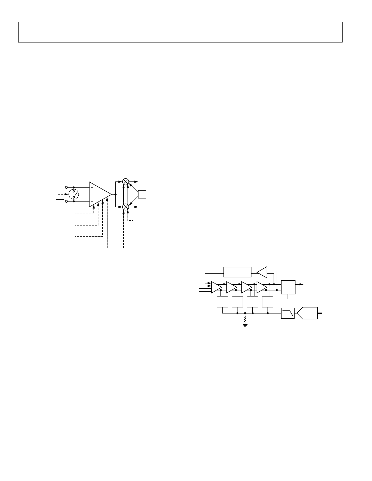
ADF7021-V
RECEIVER SECTION
RF FRONT END
The ADF7021-V is based on a fully integrated, low IF receiver
architecture. The low IF architecture facilitates a very low external
component count and does not suffer from powerline-induced
interference problems.
Figure 44 shows the structure of the receiver front end. The
many programming options allow users to trade off sensitivity,
linearity, and current consumption to best suit their application.
To achieve a high level of resilience against spurious reception,
the low noise amplifier (LNA) features a differential input.
Switch SW2 shorts the LNA input when transmit mode is
selected (Register 0, Bit DB27 = 0). This feature facilitates the
design of a combined LNA/PA matching network, avoiding the
need for an external Tx/Rx switch. See the LNA/PA Matching
section for details on the design of the matching network.
Tx/Rx SELECT
(REG 0, BIT DB27)
(REG 9, BIT S [ DB27:DB26] )
(REG 9, BIT S [ DB21:DB20] )
LNA/MIXER_ENABLE
RFIN
RFIN
LNA_MODE
(REG 9, BIT DB25)
LNA_BIAS
LNA_GAIN
(REG 8, BI T DB6)
SW2 LNA
Figure 44. RF Front End
I (TO FILTER)
LO
Q (TO FILTER)
MIXER_LINEARITY
(REG 9, BIT DB28)
08635-043
The LNA is followed by a quadrature downconversion mixer,
which converts the RF signal to the IF frequency of 100 kHz.
An important consideration is that the output frequency of the
synthesizer must be programmed to a value 100 kHz below the
center frequency of the received channel. The LNA has two
basic operating modes: high gain/low noise mode and low gain/
low power mode. To switch between these two modes, use the
LNA_MODE bit (Register 9, Bit DB25). The mixer is also configurable for either a low current mode or an enhanced linearity
mode using the MIXER_LINEARITY bit (Register 9, Bit DB28).
Based on the specific sensitivity and linearity requirements of
the application, it is recommended that the LNA_MODE bit and
the MIXER_LINEARITY bit be adjusted as shown in Tab l e 1 4 .
The gain of the LNA is configured by the LNA_GAIN bits
(Register 9, Bits[DB21:DB20]) and can be set by the user or by
the automatic gain control (AGC) logic.
IF FILTER
IF Filter Settings
Out-of-band interference is rejected by means of a fifth-order
Butterworth polyphase IF filter centered on a frequency of
100 kHz. The bandwidth of the IF filter can be programmed to
9 kHz, 13.5 kHz, or 18.5 kHz in Register 4, Bits[DB31:DB30],
and should be chosen as a compromise between interference
rejection and attenuation of the desired signal.
Rev. 0 | Page 28 of 60
If the AGC loop is disabled, the gain of the IF filter can be set to
one of three levels by using the FILTER_GAIN bits (Register 9,
Bits[DB23:DB22]). The filter gain is adjusted automatically if
the AGC loop is enabled.
IF Filter Bandwidth and Center Frequency Calibration
To compensate for manufacturing tolerances, the IF filter should
be calibrated after power-up to ensure that the bandwidth and
center frequency are correct. Coarse and fine calibration schemes
are provided to offer a choice between fast calibration (coarse
calibration) and high filter centering accuracy (fine calibration).
Coarse calibration is enabled by setting Register 5, Bit DB4 high.
Fine calibration is enabled by setting Register 6, Bit DB4 high.
For details on when it is necessary to perform a filter calibration,
and in what applications to use either a coarse calibration or
fine calibration, see the IF Filter Bandwidth Calibration section.
RSSI/AGC
The RSSI is implemented as a successive compression log amp
following the baseband (BB) channel filtering. The log amp
achieves ±3 dB log linearity. It also doubles as a limiter to
convert the signal-to-digital levels for the FSK demodulator.
The offset correction circuit uses the BBOS_CLK_DIVIDE bits
(Bits DB5:DB4] in Register 3) and should be set between 1 MHz
and 2 MHz. The RSSI level is converted for user readback and
for digitally controlled AGC by an 80-level (7-bit) flash ADC.
This level can be converted to input power in dBm. By default,
the AGC is on when powered up in receive mode.
OFFSET
CORRECTION
FSK
1
IFWR IFWR IFWR IFWR
R
Figure 45. RSSI Block Diagram
LATCHAAA
CLK
RSSI Thresholds
When the RSSI is above AGC_HIGH_THRESHOLD (Register 9,
Bits[DB17:DB11]), the gain is reduced. When the RSSI is below
AGC_LOW_THRESHOLD (Register 9, Bits[DB10:DB4]), the
gain is increased. The thresholds default to 70 (high threshold)
and 30 (low threshold) on power-up in receive mode. A delay
(set by AGC_CLK_DIVIDE in Register 3, Bits[DB31:DB26]) is
programmed to allow for settling of the loop. A value of 33 is
recommended to give an AGC update rate of 3 kHz.
The user has the option of changing the two threshold values
from the defaults of 70 and 30 (Register 9). The default AGC
setup values should be adequate for most applications. The
threshold values must be more than 30 apart for the AGC to
operate correctly.
DEMOD
ADC
RSSI
08635-044

ADF7021-V
Offset Correction Clock
In Register 3, the user should set the BBOS_CLK_DIVIDE bits
(Bits[DB5:DB4]) to give a baseband offset clock (BBOS CLK)
frequency between 1 MHz and 2 MHz.
BBOS CLK (Hz) = XTAL/(BBOS_CLK_DIVIDE)
where BBOS_CLK_DIVIDE can be set to 4, 8, 16, or 32.
AGC Information and Timing
AGC is selected by default and operates by setting the appropriate LNA and filter gain settings for the measured RSSI level.
To enter one of the LNA/mixer modes listed in Table 1 4, the
user can disable AGC by writing to Register 9. After each gain
change, the AGC loop waits for a programmed time to allow
transients to settle. This AGC update rate is set according to
AGC Update Rate (Hz) =
DIVIDECLKSEQ
(Hz)__
DIVIDECLKAGC
__
where:
SEQ_CLK_DIVIDE = 100 kHz (Register 3, Bits[DB25:DB18]).
AGC_CLK_DIVIDE is set by Register 3, Bits[DB31:DB26]. A
value of 33 is recommended.
It is recommended that AGC_CLK_DIVIDE be set to a value of
33, which allows a settling time of 333 µs for each gain change.
By using the recommended setting for AGC_CLK_DIVIDE, the
total AGC settling time is
TimeSettlingAGC
(sec)
=
ChangesGainAGCofNumber
(Hz)
RateUpdateAGC
The total AFC settling time depends on the number of AGC
gain changes during reception of a packet. A total of five gain
changes gives a worst-case AGC settling time of 5 × 333 µs. To
allow for AGC settling, the preamble length should be adjusted
accordingly.
RSSI Formula (Converting to dBm)
The RSSI formula is
Input Power (dBm) = (−130 dBm + (Readback Code +
Gain Mode Correction)) × 0.5
where:
Readback Code is given by Bit RV7 to Bit RV1 in the readback
register (see Figure 57 and the Readback Format section).
Gain Mode Correction is given by the values in Table 1 3.
The LNA gain (LG2, LG1) and filter gain (FG2, FG1) values
are also obtained from the readback register, as part of an RSSI
readback.
Table 13. Gain Mode Correction
LNA Gain
(LG2, LG1)
H (1, 0) H (1, 0) 0
M (0, 1) H (1, 0) 24
M (0, 1) M (0, 1)
M (0, 1) L (0, 0)
L (0, 0) L (0, 0) 86
Filter Gain
(FG2, FG1)
Gain Mode
Correction
38
58
An additional factor should be introduced to account for losses
in the front-end-matching network/antenna.
Table 14. LNA/Mixer Modes (Register 9 Settings)
Sensitivity (2FSK,
LNA_MODE
Receiver Mode
High Sensitivity
Mode (Default)
Enhanced Linearity,
High Gain
Medium Gain 1 10 0 −108 17.9 −13.5
Enhanced Linearity,
Medium Gain
Low Gain 1 3 0 −99 17.9 −5
Enhanced Linearity,
Low Gain
(Bit DB25)
0 30 0 −116.5 20.1 −24
0 30 1 −113 20.1 −20
1 10 1 −102 17.9 −9
1 3 1 −91 17.9 −3
LNA_GAIN
(Bits[DB21:DB20])
MIXER_LINEARITY
(Bit DB28)
Data Rate = 4.8 kbps,
f
= 4 kHz) (dBm)
DEV
Rx Current
Consumption (mA)
Input IP3
(dBm)
Rev. 0 | Page 29 of 60
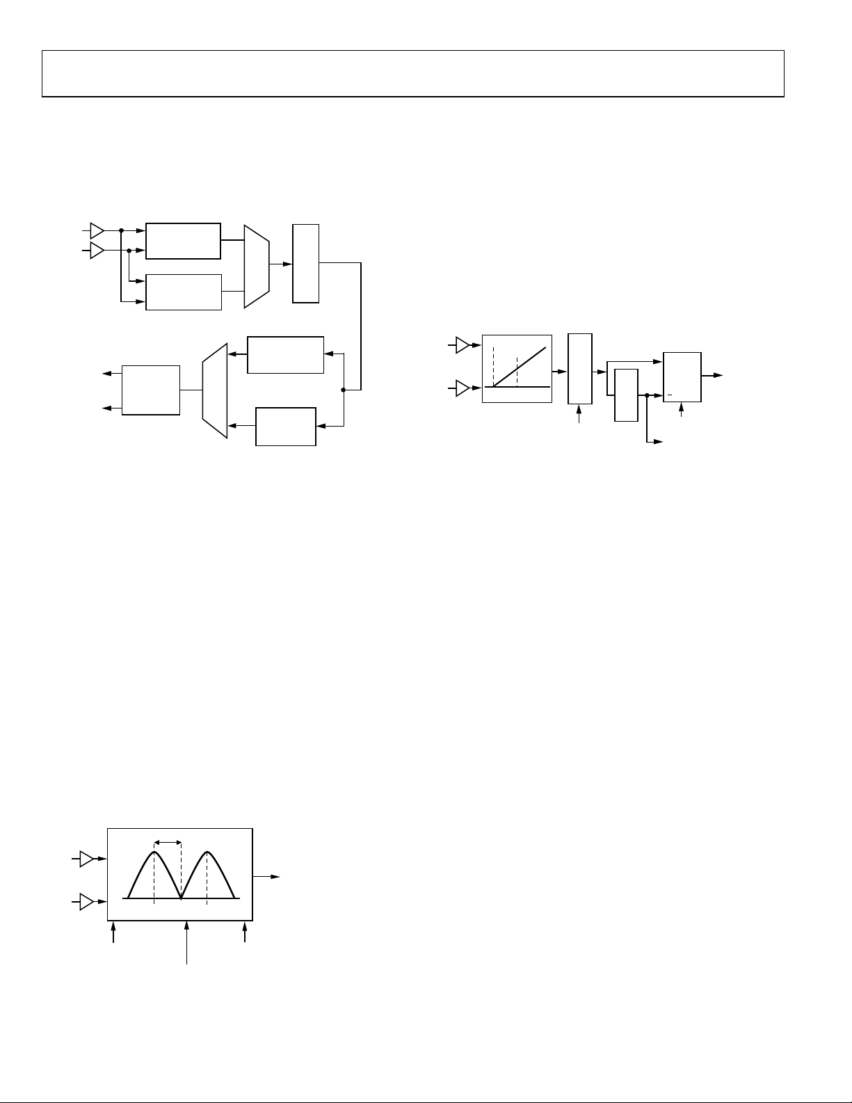
ADF7021-V
R
DEMODULATION, DETECTION, AND CDR
System Overview
An overview of the demodulation, detection, and clock and
data recovery (CDR) of the received signal on the ADF7021-V
is shown in Figure 46.
LIMITERS
I
Q
TxRxDATA
TxRxCLK
Figure 46. Overview of Demodulation, Detection, and CDR Process
The quadrature outputs of the IF filter are first limited and
then fed to either the correlator FSK demodulator or to the
linear FSK demodulator. The correlator demodulator is used
to demodulate 2FSK, 3FSK, and 4FSK. The linear demodulator
is used for frequency measurement and is enabled when the
AFC loop is active. The linear demodulator can also be used
to demodulate 2FSK.
Following the demodulator, a digital postdemodulator filter
removes excess noise from the demodulator signal output.
Threshold/slicer detection is used for data recovery of 2FSK and
4FSK. Data recovery of 3FSK can be implemented using either
threshold detection or Viterbi detection.
An on-chip CDR PLL is used to resynchronize the received bit
stream to a local clock. It outputs the retimed data and clock on
the TxRxDATA and TxRxCLK pins, respectively.
Correlator Demodulator
The correlator demodulator can be used for 2FSK, 3FSK, and
4FSK demodulation. Figure 47 shows the operation of the
correlator demodulator for 2FSK.
I
LIMITERS
Q
CORRELATOR
DEMODULATOR
LINEAR
DEMODULATOR
CLOCK
AND
DATA
RECOVERY
FREQUENCY COR
DISCRIM BW
IF –
IF
f
DEV
ELATOR
IF +
MUX
f
DEV
MUX
THRESHOLD
DETECTION
2FSK/3FSK/4FSK
VITERBI
DETECTION
3FSK
OUTPUT LEVELS:
2FSK = +1, –1
3FSK = +1, 0, –1
4FSK = +3, +1, –1, –3
POST
DEMOD FILTER
08635-045
The quadrature outputs of the IF filter are first limited and then
fed to a digital frequency correlator that performs filtering and
frequency discrimination of the 2FSK/3FSK/4FSK spectrum.
For 2FSK modulation, data is recovered by comparing the
output levels from two correlators. The performance of this
frequency discriminator approximates that of a matched filter
detector, which is known to provide optimum detection in the
presence of additive white Gaussian noise (AWGN). This
method of FSK demodulation provides approximately 3 dB to
4 dB better sensitivity than a linear demodulator.
Linear Demodulator
Figure 48 shows a block diagram of the linear demodulator.
I
LEVEL
LIMITERS
Q
IF
FREQUENCY
LINEAR
DISCRIMINATOR
REG 4, BITS [DB29: DB20]
FILTER
POST DEMOD
ENVELOPE
DETECTOR
+
2FSK RxDATA
SLICER
2FSK
RxCLK
FREQUENCY
READBACK
AND AFC LOOP
Figure 48. Block Diagram of Linear FSK Demodulator
A digital frequency discriminator provides an output signal that
is linearly proportional to the frequency of the limiter outputs.
The discriminator output is filtered and averaged using a combined averaging filter and envelope detector. The demodulated
2FSK data from the postdemodulator filter is recovered by
slicing against the output of the envelope detector, as shown in
Figure 48. This method of demodulation corrects for frequency
errors between the transmitter and receiver when the received
spectrum is close to or within the IF bandwidth. This envelope
detector output is also used for AFC readback and provides the
frequency estimate for the AFC control loop.
Postdemodulator Filter
A second-order, digital low-pass filter removes excess noise from
the demodulated bit stream at the output of the discriminator.
The bandwidth of this postdemodulator filter is programmable
and must be optimized for the user’s data rate and the received
modulation type. If the bandwidth is too narrow, performance
degrades due to intersymbol interference (ISI). If the bandwidth
is too wide, excess noise degrades the performance of the receiver.
The POST_DEMOD_BW bits (Register 4, Bits[DB29:DB20])
set the bandwidth of this filter.
08635-047
REG 4, BIT S [DB19: DB10 ]
DISCRIMINATOR_BW
REG 4, BIT DB7
DOT_PRODUCT
REG 4, BITS[DB9:DB8]
Rx_INVERT
8635-046
Figure 47. 2FSK Correlator FSK Demodulator Operation
Rev. 0 | Page 30 of 60

ADF7021-V
2FSK Bit Slicer/Threshold Detection
2FSK demodulation can be implemented using the correlator
FSK demodulator or the linear FSK demodulator. In both cases,
threshold detection is used for data recovery at the output of the
postdemodulator filter.
The output signal levels of the correlator demodulator are always
centered about 0. Therefore, the slicer threshold level can be
fixed at 0, and the demodulator performance is independent of
the run-length constraints of the transmit data bit stream. This
results in robust data recovery that does not suffer from the
classic baseline wander problems that exist in more traditional
FSK demodulators.
When the linear demodulator is used for 2FSK demodulation,
the output of the envelope detector is used as the slicer threshold,
and this output tracks frequency errors that are within the IF
filter bandwidth.
3FSK and 4FSK Threshold Detection
4FSK demodulation is implemented using the correlator
demodulator followed by the postdemodulator filter and
threshold detection. The output of the postdemodulator filter
is a four-level signal that represents the transmitted symbols
(−3, −1, +1, +3). Threshold detection of 4FSK requires three
threshold settings: one that is always fixed at 0 and two that are
programmable and are symmetrically placed above and below 0
using the 3FSK/4FSK_SLICER_THRESHOLD bits (Register 13,
Bits[DB10:DB4]).
3FSK demodulation is implemented using the correlator demodulator, followed by a postdemodulator filter. The output of the
postdemodulator filter is a three-level signal that represents the
transmitted symbols (−1, 0, +1). Data recovery of 3FSK can be
implemented using threshold detection or Viterbi detection.
Threshold detection is implemented using two thresholds that
are programmable and are symmetrically placed above and
below 0 using the 3FSK/4FSK_SLICER_THRESHOLD bits
(Register 13, Bits[DB10:DB4]).
3FSK Viterbi Detection
Viterbi detection of 3FSK operates on a four-state trellis and is
implemented using two interleaved Viterbi detectors operating
at half the symbol rate. The Viterbi detector is enabled by
Register 13, Bit DB11.
To facilitate different run-length constraints in the transmitted
bit stream, the Viterbi path memory length is programmable in
steps of 4 bits, 6 bits, 8 bits, or 32 bits by setting the VITERBI_
PATH_MEMORY bits (Register 13, Bits[DB14:DB13]). This
value should be set equal to or greater than the maximum
number of consecutive 0s in the interleaved transmit bit stream.
When used with Viterbi detection, the receiver sensitivity
for 3FSK is typically 3 dB greater than that obtained using
threshold detection. When the Viterbi detector is enabled,
however, the receiver bit latency is increased by twice the
Viterbi path memory length.
Clock and Data Recovery (CDR)
An oversampled digital clock and data recovery (CDR) PLL is
used to resynchronize the received bit stream to a local clock in
all modulation modes. The oversampled clock rate of the PLL
(CDR CLK) must be set at 32 times the symbol rate (see the
Register 3—Transmit/Receive Clock Register section). The maximum data/symbol rate tolerance of the CDR PLL is determined
by the number of zero-crossing symbol transitions in the transmitted packet. For example, if using 2FSK with a 101010 preamble,
a maximum tolerance of ±3.0% of the data rate is achieved.
However, this tolerance is reduced during recovery of the
remainder of the packet, where symbol transitions may not be
guaranteed to occur at regular intervals. To maximize the data
rate tolerance of the CDR, some form of encoding and/or data
scrambling is recommended that guarantees a number of
transitions at regular intervals.
For example, using 2FSK with Manchester-encoded data
achieves a data rate tolerance of ±2.0%.
The CDR PLL is designed for fast acquisition of the recovered
symbols during preamble and typically achieves bit synchronization within five-symbol transitions of preamble.
In 4FSK modulation, the tolerance using the +3, −3, +3, −3
preamble is ±3% of the symbol rate (or ±1.5% of the data rate).
However, this tolerance is reduced during recovery of the
remainder of the packet, where symbol transitions may not
be guaranteed to occur at regular intervals. To maximize the
symbol/data rate tolerance of the CDR, the remainder of the
4FSK packet should be constructed so that the transmitted
symbols retain close to dc-free properties by using data scrambling and/or by inserting specific dc-balancing symbols into the
transmitted bit stream at regular intervals, such as after every
8 or 16 symbols.
In 3FSK modulation, the linear convolutional encoder scheme
guarantees that the transmitted symbol sequence is dc-free,
facilitating symbol detection. However, Tx data scrambling is
recommended to limit the run length of 0 symbols in the
transmit bit stream. Using 3FSK, the CDR data rate tolerance is
typically ±0.5%.
Rev. 0 | Page 31 of 60

ADF7021-V
(
)
RECEIVER SETUP
Correlator Demodulator Setup
To enable the correlator for various modulation modes, see
Tabl e 15 .
Table 15. Enabling the Correlator Demodulator
DEMOD_SCHEME
Received Modulation
2FSK 001
3FSK 010
4FSK 011
To optimize receiver sensitivity, the correlator bandwidth must
be optimized for the specific deviation frequency and modulation used by the transmitter. The discriminator bandwidth is
controlled by Register 4, Bits[DB19:DB10], and is defined as
where:
DEMOD CLK is as defined in the Register 3—Transmit/Receive
Clock Register section.
K is set for each modulation mode as follows:
For 2FSK,
=
⎜
f
⎝
⎛
×
⎜
RoundK
For 3FSK,
=
⎜
f
2
×
⎝
⎛
×
⎜
RoundK
For 4FSK,
⎛
4FSK
⎜
⎜
⎝
RoundK
=
where:
Round is rounded to the nearest integer.
Round
is rounded to the nearest of the following integers:
4FSK
32, 31, 28, 27, 24, 23, 20, 19, 16, 15, 12, 11, 8, 7, 4, 3.
is the transmit frequency deviation in Hz. For 4FSK, f
f
DEV
is the frequency deviation used for the ±1 symbols (that is, the
inner frequency deviations).
To optimize the coefficients of the correlator, Register 4, Bit DB7
and Register 4, Bits[DB9:DB8] must also be assigned. The value
of these bits depends on whether K is odd or even. These bits
are assigned according to Table 16 and Tabl e 17 .
Table 16. Assignment of Correlator K Value for 2FSK and 3FSK
K K/2 (K + 1)/2
Even Even N/A 0 00
Even Odd N/A 0 10
Odd N/A Even 1 00
Odd N/A Odd 1 10
(Register 4, Bits[DB6:DB4])
BWTORDISCRIMINA
3
⎞
10100
⎟
⎟
DEV
⎠
3
⎞
10100
⎟
⎟
DEV
⎠
3
⎞
×
10100
⎟
⎟
×
f
4
DEV
⎠
Register 4,
Bit DB7
×=KCLKDEMOD
3
10400_×
Register 4,
Bits[DB9:DB8]
DEV
Table 17. Assignment of Correlator K Value for 4FSK
K Register 4, Bit DB7 Register 4, Bits[DB9:DB8]
Even 0 00
Odd 1 00
Linear Demodulator Setup
The linear demodulator can be used for 2FSK demodulation. To
enable the linear demodulator, set the DEMOD_SCHEME bits
(Register 4, Bits[DB6:DB4]) to 000.
Postdemodulator Filter Setup
The 3 dB bandwidth of the postdemodulator filter should be
set according to the received modulation type and data rate.
The bandwidth is controlled by Register 4, Bits[DB29:DB20]
and is given by
11
f
××=π2
CUTOFF
CLKDEMOD
where f
BWDEMODPOST
__
is the target 3 dB bandwidth in Hz of the post-
CUTOFF
demodulator filter.
Table 18. Postdemodulator Filter Bandwidth Settings for
2FSK/3FSK/4FSK Modulation Schemes
Received
Modulation
2FSK 0.75 × data rate
3FSK 1 × data rate
4FSK 1.6 × symbol rate (0.8 × data rate)
Postdemodulator Filter Bandwidth,
f
(Hz)
CUTOFF
3FSK Viterbi Detector Setup
The Viterbi detector can be used for 3FSK data detection; it is
activated by setting Register 13, Bit DB11, to Logic 1.
The Viterbi path memory length is programmable in steps of
4, 6, 8, or 32 bits (VITERBI_PATH_MEMORY, Register 13,
Bits[DB14:DB13]). The path memory length should be set
equal to or greater than the maximum number of consecutive
0s in the interleaved transmit bit stream.
The Viterbi detector also uses threshold levels to implement the
maximum likelihood detection algorithm. These thresholds are
programmable via the 3FSK/4FSK_SLICER_THRESHOLD bits
(Register 13, Bits[DB10:DB4]).
These bits are assigned as follows:
3FSK/4FSK_SLICER_THRESHOLD =
⎛
⎜
×
75
⎜
⎝
__
3
×
10100
⎞
×
KDEVIATIONFREQUENCYTx
⎟
⎟
⎠
where K is the value calculated for correlator discriminator
bandwidth.
3FSK Threshold Detector Setup
To activate threshold detection of 3FSK, Register 13, Bit DB11,
should be set to Logic 0. The 3FSK/4FSK_SLICER_THRESHOLD
bits (Register 13, Bits[DB10:DB4]) should be set as described in
the 3FSK Viterbi Detector Setup section.
Rev. 0 | Page 32 of 60

ADF7021-V
3FSK CDR Setup
In 3FSK, a transmit preamble of at least 40 bits of continuous
1s is recommended to ensure a maximum number of symbol
transitions for the CDR to acquire lock.
The clock and data recovery for 3FSK requires a number of
parameters in Register 13 to be set (see Tabl e 19).
4FSK Threshold Detector Setup
The threshold for the 4FSK detector is set using the
3FSK/4FSK_SLICER_THRESHOLD bits (Register 13,
Bits[DB10:DB4]). The threshold should be set as follows:
3FSK/4FSK_SLICER_THRESHOLD =
78
⎛
⎜
×
⎜
⎝
3
×
10100
⎞
×
K Deviation Tx Outer 4FSK
⎟
⎟
⎠
where K is the value calculated for correlator discriminator
bandwidth.
FSK DEMODULATOR OPTIMIZATION
2FSK Preamble
The recommended preamble bit pattern for 2FSK, GFSK, and
RC2FSK is a dc-free pattern (such as a 10101010… pattern).
Preamble patterns with longer run-length constraints (such as
Table 19. 3FSK CDR Settings
Parameter (Register 13) Recommended Setting Purpose
PHASE_CORRECTION (Bit DB12) 1 Phase correction is on
3FSK_CDR_THRESHOLD (Bits[DB21:DB15])
3FSK_PREAMBLE_TIME_VALIDATE (Bits[DB25:DB22]) 15 Preamble detector time qualifier
Table 20. Preamble Bit Length for 2FSK Modulation
Sensitivity Degradation
Demodulator
from Specifications
Correlator (AFC off)
Mod index = 2 0 dB ±30% × f
Mod index = 1 0 dB ±25% × f
Mod index = 0.5 0 dB ±20% × f
Linear (AFC off)
f
= 4.2 kHz 3 dB ±0.5 × IFBW
DEV
f
= 2.2 kHz 3 dB ±0.5 × IFBW
DEV
f
= 1.6 kHz 3 dB ±0.5 × IFBW
DEV
Correlator (AFC on) 2 dB AFC pull-in range
Linear (AFC on) 3 dB AFC pull-in range
Correlator + bypass CDR (AFC off) 2 dB to 3 dB
1
This value is generally true; however, some sensitivity degradation may occur close to the edge of the IF filter.
2
Limited to ±0.5 × IFBW or AFC pull-in range, whichever is less.
3
Dependent on modulation index and f
minimum preamble length increases as the modulation index and f
4
Dependent on the performance of the symbol timing recovery module on the external microcontroller.
5
Depends on the pulse width mark/space ratio of Logic 1 to Logic 0 that the symbol timing recovery scheme on the external microcontroller can tolerate. In this mode,
the mark/space ratio of the recovered bit stream increases with frequency error. In the absence of frequency error, the mark/space ratio is 50:50, that is, the width of a
Logic 1 is the same as the width of a Logic 0.
. At higher modulation indexes (1.0 or greater) and higher f
DEV
4
⎛
⎜
×
62
⎜
⎝
where K is the value calculated for correlator
discriminator bandwidth.
are reduced.
DEV
Rev. 0 | Page 33 of 60
11001100…) can also be used, but result in a longer synchronization time of the received bit stream in the receiver. The
preamble must allow enough bits for AGC settling of the
receiver and CDR acquisition (see Tabl e 20 ).
The remaining fields that follow the preamble do not need to
use dc-free coding. For these fields, the ADF7021-V can accommodate coding schemes with a run length of greater than eight
bits without any performance degradation. Refer to the AN-915
Application Note for more information.
4FSK Preamble and Data Coding
The recommended preamble bit pattern for 4FSK is a repeating
00100010… bit sequence. This two-level sequence of repeating
−3, +3, −3, +3 symbols is dc-free and maximizes the symbol
timing performance and data recovery of the 4FSK preamble
in the receiver. The minimum recommended length of the
preamble is 32 bits (16 symbols).
The remainder of the 4FSK packet should be constructed so
that the transmitted symbols retain close to a dc-free balance by
using data scrambling and/or by inserting specific dc-balancing
symbols in the transmitted bit stream at regular intervals, such
as after every 8 or 16 symbols.
Sets CDR decision threshold levels
⎞
__
3
×
10100
×
K DEVIATIONFREQUENCYTx
⎟
⎟
⎠
Rx Frequency Error
Tolerance (1% P E R)
16
DEV
16
DEV
16
DEV
Minimum Preamble (Bits)
±50% × f
1
1
112
1
128
2
2
96 to 128
5
DEV
(>4.0 kHz), the minimum preamble length is 96 bits. The
DEV
64
96 to 128
8
3

ADF7021-V
Correlator Demodulator and Low Modulation Indexes
The modulation index in 2FSK is defined as
f
×=2
IndexModulation
DEV
RateData
The receiver sensitivity performance and receiver frequency
tolerance can be maximized at low modulation indexes by
increasing the discriminator bandwidth of the correlator
demodulator. For modulation indexes of less than 0.4, it is
recommended that the correlator bandwidth be doubled by
calculating K as follows:
3
100
×
f
DEV
⎞
⎟
⎟
⎠
=
⎜
2
⎝
⎛
⎜
RoundK
The DISCRIMINATOR_BW value in Register 4 should be
recalculated using the new K value. Figure 29 illustrates the
improved sensitivity that can be achieved for 2FSK modulation,
at low modulation indexes, by doubling the correlator bandwidth.
AFC OPERATION
The ADF7021-V also supports a real-time AFC loop that is
used to remove frequency errors due to mismatches between
the transmit and receive crystals/TCXOs. The AFC loop uses
the linear frequency discriminator block to estimate frequency
errors. The linear FSK discriminator output is filtered and
averaged to remove the FSK frequency modulation using a
combined averaging filter and envelope detector. In receive
mode, the output of the envelope detector provides an estimate
of the average IF frequency.
The two methods of AFC supported on the ADF7021-V are
external AFC and internal AFC.
External AFC
With external AFC, the user reads back the frequency information through the ADF7021-V serial port and applies a
frequency correction value to the synthesizer-N divider.
The frequency information is obtained by reading the
signed, 16-bit AFC readback value, as described in the
Readback Format section, and by applying the following
formula:
Frequency Readback (Hz) = (AFC READBACK ×
DEMOD CLK)/2
Although the AFC readback value is a signed number, under
normal operating conditions, it is positive. In the absence of
frequency errors, the frequency readback value is equal to the
IF frequency of 100 kHz.
18
Internal AFC
The ADF7021-V supports a real-time, internal, automatic
frequency control loop. In this mode, an internal control loop
automatically monitors the frequency error and adjusts the
synthesizer-N divider using an internal proportional integral
(PI) control loop.
The internal AFC control loop parameters are controlled in
Register 10. The internal AFC loop is activated by setting
Bit DB4 in Register 10 to 1. A scaling coefficient must also be
entered, based on the crystal frequency in use. This is set up
using Bits[DB16:DB5] in Register 10 and should be calculated
as follows:
24
⎛
__
=
⎜
RoundFACTORSCALINGAFC
⎜
XTAL
⎝
⎞
×
5002
⎟
⎟
⎠
Maximum AFC Range
The maximum frequency correction range of the AFC loop
is programmable using Register 10, Bits[DB31:DB24]. The
maximum AFC correction range is the difference in frequency
between the upper and lower limits of the AFC tuning range.
For example, if the maximum AFC correction range is set to
10 kHz, the AFC can adjust the receiver LO within the f
±
LO
5 kHz range.
However, when RF_DIVIDE_BY_2 (Register 1, Bit DB18) is
enabled, the programmed range is halved. The user should
account for this halving by doubling the programmed maximum AFC range.
The recommended maximum AFC correction range should be
≤1.5 × IF filter bandwidth. If the maximum frequency correction
range is set to be >1.5 × IF filter bandwidth, the attenuation of
the IF filter can degrade the AFC loop sensitivity.
The adjacent channel rejection (ACR) performance of the receiver
can be degraded when AFC is enabled and the AFC correction
range is close to or greater than the IF filter bandwidth. However,
because the AFC correction range is programmable, the user
can trade off AFC correction range and ACR performance of
the receiver.
When AFC errors are removed using either the internal or
external AFC, further improvement in receiver sensitivity can
be obtained by reducing the IF filter bandwidth using the
IF_FILTER_BW bits (Register 4, Bits[DB31:DB30]).
Rev. 0 | Page 34 of 60

ADF7021-V
AUTOMATIC SYNC WORD DETECTION (SWD)
The ADF7021-V also supports automatic detection of the sync
or ID fields. To activate this mode, the sync (or ID) word must
be preprogrammed into the ADF7021-V. In receive mode, this
preprogrammed word is compared to the received bit stream.
When a valid match is identified, the external SWD pin is
asserted by the ADF7021-V on the next Rx clock pulse.
This feature can be used to alert the microprocessor that a
valid channel has been detected. It relaxes the computational
requirements of the microprocessor and reduces the overall
power consumption.
The SWD signal can also be used to frame the received packet
by staying high for a preprogrammed number of bytes. The data
packet length can be set in Register 12, Bits[DB15:DB8].
The SWD pin status can be configured by setting Bits[DB7:DB6]
in Register 12. Bits[DB5:DB4] in Register 11 are used to set the
length of the sync/ID word, which can be 12, 16, 20, or 24 bits
long. A value of 24 bits is recommended to minimize false sync
word detection in the receiver that can occur during recovery of
the remainder of the packet or when a noise/no signal is present
at the receiver input. The transmitter must transmit the sync
byte MSB first, LSB last to ensure proper alignment in the
receiver sync-byte-detection hardware.
An error tolerance parameter can also be programmed that
accepts a valid match when up to three bits of the word are
incorrect. The error tolerance value is assigned in Register 11,
Bits[DB7:DB6].
Rev. 0 | Page 35 of 60

ADF7021-V
APPLICATIONS INFORMATION
IF FILTER BANDWIDTH CALIBRATION
The IF filter should be calibrated on every power-up in receive
mode to correct for errors in the bandwidth and filter center
frequency due to process variations. The automatic calibration
requires no external intervention when it is initiated by a write
to Register 5. Depending on numerous factors, such as IF filter
bandwidth, received signal bandwidth, and temperature variation, the user must determine whether to carry out a coarse
calibration or a fine calibration.
The performance of both calibration methods is shown in
Tabl e 21 .
Table 21. IF Filter Calibration Specifications
Filter Calibration
Method
Coarse Calibration 100 kHz ± 2.5 kHz 200 μs
Fine Calibration 100 kHz ± 0.6 kHz 8.2 ms
1
After calibration.
Center Frequency
Accuracy
1
Calibration Setup
IF filter calibration is initiated by writing to Register 5 and
setting the IF_CAL_COARSE bit (Bit DB4). This initiates a
coarse filter calibration. If the IF_FINE_CAL bit (Register 6,
Bit DB4) has already been set high, the coarse calibration is
followed by a fine calibration; otherwise, the calibration ends.
When initiated by writing to the part, calibration is performed
automatically without user intervention. The calibration time is
200 µs for coarse calibration and 8.2 ms for fine calibration, during
which time the ADF7021-V should not be accessed. The IF
filter calibration logic requires that the IF_FILTER_DIVIDER
bits (Register 5, Bits[DB13:DB5]) be set such that
(Hz)
XTAL
__
DIVIDERFILTERIF
=
kHz50
The fine calibration uses two internally generated tones at certain
offsets around the IF filter. The two tones are attenuated by the
IF filter, and the level of this attenuation is measured using the
RSSI. The filter center frequency is adjusted to allow equal
attenuation of both tones. The attenuation of the two test tones
is then remeasured. This process continues for a maximum of
10 RSSI measurements, at which point the calibration algorithm
sets the IF filter center frequency to within 0.6 kHz of 100 kHz.
The frequency of these tones is set in Register 6 by the
IF_CAL_LOWER_TONE_DIVIDE bits (Bits[DB12:DB5]) and
the IF_CAL_UPPER_TONE_DIVIDE bits (Bits[DB20:DB13]),
as shown in the following equations.
Calibration
Time (Typ)
Lower Tone Frequency (kHz) =
XTAL
2×VIDEER_TONE_DIIF_CAL_LOW
Upper Tone Frequency (kHz) =
XTAL
2×VIDEER_TONE_DIIF_CAL_UPP
It is recommended that the lower tone and the upper tone be set
as shown in Tab l e 2 2 .
Table 22. IF Filter Fine Calibration Tone Frequencies
IF Filter
Bandwidth (kHz)
9 78.1 116.3
13.5 79.4 116.3
18.5 78.1 119
Lower Tone
Frequency (kHz)
Upper Tone
Frequency (kHz)
Because the filter attenuation is slightly asymmetrical, it is
necessary to have a small offset in the filter center frequency to
provide near equal rejection at the upper and lower adjacent
channels. The calibration tones listed in Ta b le 2 2 provide this
small positive offset in the IF filter center frequency.
In some applications, an offset may not be required, and the
user may wish to center the IF filter at 100 kHz exactly. In this
case, the user can alter the tone frequencies from those given in
Tabl e 22 to adjust the fine calibration result.
The calibration algorithm adjusts the filter center frequency and
measures the RSSI 10 times during the calibration. The time for
an adjustment plus RSSI measurement is given by
TimenCalibratioToneIF =
LL_TIMEIF_CAL_DWE
CLKSEQ
It is recommended that the IF tone calibration time be at least
800 µs. The total time for the IF filter fine calibration is given by
IF Filter Fine Calibration Time = IF Tone Calibration Time × 10
When to Use Coarse Calibration
It is recommended that a coarse calibration be performed on
every power-up in receive mode. This calibration typically takes
200 µs. The FILTER_CAL_COMPLETE signal from MUXOUT
(set using Bits[DB31:DB29] in Register 0) can be used to monitor
the filter calibration duration or to signal the end of calibration.
The ADF7021-V should not be accessed during calibration.
Rev. 0 | Page 36 of 60

ADF7021-V
V
A
A
When to Use Fine Calibration
In cases where the receive signal bandwidth is very close to the
bandwidth of the IF filter, it is recommended that a fine filter
calibration be performed every time that the unit powers up in
receive mode.
A fine calibration should be performed if
OBW + Coarse Calibration Variation > IF_FILTER_BW
where:
OBW is the 99% occupied bandwidth of the transmit signal.
Coarse Calibration Variation is 2.5 kHz.
IF_FILTER_BW is set by Register 4, Bits[DB31:DB30].
The FILTER_CAL_COMPLETE signal from MUXOUT (set by
Register 0, Bits[DB31:DB29]) can be used to monitor the filter
calibration duration or to signal the end of calibration. A coarse
filter calibration is automatically performed prior to a fine filter
calibration.
When to Use Single Fine Calibration
In applications where the receiver powers up numerous times
in a short period, it is necessary to perform fine calibration only
once, on the initial power-up in receive mode.
After the initial coarse calibration and fine calibration, the result
of the fine calibration can be read back through the serial interface using the FILTER_CAL_READBACK result (see the Filter
Bandwidth Calibration Readback section). On subsequent
power-ups in receive mode, the filter is manually adjusted using
the previous fine filter calibration result. This manual adjustment
is performed using the IF_FILTER_ADJUST bits (Register 5,
Bits[DB19:DB14]).
This method should only be used if the successive power-ups in
receive mode are over a short duration, during which time there
is little variation in temperature (<15°C).
IF Filter Variation with Temperature
When calibrated, the filter center frequency can vary with changes
in temperature. If the ADF7021-V is used in an application where
it remains in receive mode for a considerable length of time, the
user must consider this variation of filter center frequency with
temperature. This variation is typically 1 kHz per 20°C, which
means that if a coarse filter calibration and fine filter calibration
are performed at 25°C, the initial maximum error is ±0.5 kHz,
and the maximum possible change in the filter center frequency
over temperature (−40°C to +85°C) is ±3.25 kHz. This gives a
total error of ±3.75 kHz.
If the receive signal occupied bandwidth is considerably
narrower than the IF filter bandwidth, the variation of filter
center frequency over the operating temperature range may
not be an issue. However, if the IF filter bandwidth is not wide
enough to tolerate the variation with temperature, a periodic
filter calibration can be performed or, alternatively, the on-chip
temperature sensor can be used to determine when a filter calibration is necessary by monitoring for changes in temperature.
LNA/PA MATCHING
The ADF7021-V exhibits optimum performance in terms of
sensitivity, transmit power, and current consumption only if its
RF input and output ports are properly matched to the antenna
impedance. For cost-sensitive applications, the ADF7021-V is
equipped with an internal Tx/Rx switch that facilitates the use
of a simple, combined passive LNA/PA matching network.
Alternatively, an external Tx/Rx switch such as the ADG919 can
be used, which yields a slightly improved receiver sensitivity
and lower transmitter power consumption.
Internal Tx/Rx Switch
Figure 49 shows the ADF7021-V in a configuration where
the internal Tx/Rx switch is used with a combined LNA/PA
matching network. This is the configuration used on the
EVAL-ADF7021-VDBxZ evaluation board. For most applications, the slight performance degradation of 1 dB to 2 dB
caused by the internal Tx/Rx switch is acceptable, allowing
the user to take advantage of the cost-saving potential of this
solution. The design of the combined matching network must
compensate for the reactance presented by the networks in the
Tx and the Rx paths, taking the state of the Tx/Rx switch into
consideration.
BAT
L1
C1
NTENN
OPTIONAL
BPF OR LPF
Figure 49. ADF7021-V with Internal Tx/Rx Switch
Z
OPT
Z
IN
C
A
L
A
ZIN_RFIN
C
B
The procedure typically requires several iterations until an acceptable compromise is reached. The successful implementation of
a combined LNA/PA matching network for the ADF7021-V is
critically dependent on the availability of an accurate electrical
model for the PCB. In this context, the use of a suitable CAD
package is strongly recommended. To avoid this effort, a small
form-factor reference design for the ADF7021-V is provided,
including matching and harmonic filter components. The design is
on a 4-layer PCB. Gerber files are available at www.analog.com.
_PA
_RFIN
ADF7021-V
RFOUT
RFIN
RFIN
PA
LNA
08635-048
Rev. 0 | Page 37 of 60

ADF7021-V
V
External Tx/Rx Switch
Figure 50 shows a configuration using an external Tx/Rx switch.
This configuration allows independent optimization of the
matching and filter network in the transmit and receive paths.
Therefore, it is more flexible and less difficult to design than the
configuration using the internal Tx/Rx switch. The PA is biased
through Inductor L1, whereas C1 blocks dc current. Together,
L1 and C1 form the matching network that transforms the source
impedance into the optimum PA load impedance, Z
BAT
ADG919
ANTENNA
Rx/Tx – SEL ECT
Figure 50. ADF7021-V with External Tx/Rx Switch
Z
_PA depends on various factors, such as the required out-
OPT
OPTIONAL
OPTIONAL
BPF
(SAW)
LPF
C
C
C1
A
B
Z
OPT
Z
IN
L
ZIN_RFIN
L1
_PA
_RFIN
A
ADF7021-V
RFOUT
RFIN
RFIN
OPT
_PA.
PA
LNA
put power, the frequency range, the supply voltage range, and
the temperature range. Selecting an appropriate Z
_PA helps
OPT
to minimize the Tx current consumption in the application.
The AN-764 Application Note and the AN-859 Application
Note contain a number of Z
_PA values for representative
OPT
conditions. Under certain conditions, however, it is recommended that a suitable Z
_PA value be obtained by means
OPT
of a load-pull measurement.
Due to the differential LNA input, the LNA matching network
must be designed to provide both a single-ended-to-differential
conversion and a complex, conjugate impedance match. The network with the lowest component count that can satisfy these
requirements is the configuration shown in Figure 50, consisting of two capacitors and one inductor.
Depending on the antenna configuration, the user may need a
harmonic filter at the PA output to satisfy the spurious emission
requirement of the applicable government regulations. The harmonic filter can be implemented in various ways, for example, a
discrete LC pi or T-stage filter. The immunity of the ADF7021-V
to strong out-of-band interference can be improved by adding a
band-pass filter in the Rx path. Alternatively, the ADF7021-V
blocking performance can be improved by selecting one of the
enhanced linearity modes, as described in Tabl e 14.
IMAGE REJECTION CALIBRATION
The image channel in the ADF7021-V is 200 kHz below the
desired signal. The polyphase filter rejects this image with an
asymmetric frequency response. The image rejection (IR)
08635-049
performance of the receiver is dependent on how well matched
the I and Q signals are in amplitude and how well matched the
quadrature is between them (that is, how close to 90° apart they
are). The uncalibrated image rejection performance is approximately 29 dB (at 460 MHz). However, it is possible to improve
this performance by as much as 20 dB by finding the optimum
I/Q gain and phase adjust settings.
Calibration Using Internal RF Source
With the LNA powered off, an on-chip generated, low level RF
tone is applied to the mixer inputs. The LO is adjusted to make
the tone fall at the image frequency where it is attenuated by the
image rejection of the IF filter. The power level of this tone is
then measured using the RSSI readback. The I/Q gain and phase
adjust DACs (Register 5, Bits[DB31:DB20]) are adjusted and the
RSSI is remeasured. This process is repeated until the optimum
values for the gain and phase adjust are found that provide the
lowest RSSI readback level, thereby maximizing the image
rejection performance of the receiver.
Using the internal RF source, the RF frequencies that can be
used for image calibration are programmable and are odd
multiples of the reference frequency.
Calibration Using External RF Source
IR calibration can also be implemented using an external RF
source. The IR calibration procedure is the same as that used for
the internal RF source, except that an RF tone is applied to the
LNA input.
Calibration Procedure and Setup
The IR calibration algorithm available from Analog Devices, Inc., is
based on a low complexity, 2D optimization algorithm that can
be implemented in an external microprocessor or microcontroller.
To enable the internal RF source, the IR_CAL_SOURCE_DRIVE_
LEVEL bits (Register 6, Bits[DB29:DB28]) should be set to the
maximum level. The LNA should be set to its minimum gain
setting, and the AGC should be disabled if the internal RF source
is being used. Alternatively, an external RF source can be used.
The magnitude of the phase adjust is set using the IR_PHASE_
ADJUST_MAG bits (Register 5, Bits[DB23:DB20]). This correction can be applied to either the I or Q channel, depending on
the value of the IR_PHASE_ADJUST_DIRECTION bit
(Register 5, Bit DB24).
The magnitude of the I/Q gain is adjusted using the IR_GAIN_
ADJUST_MAG bits (Register 5, Bits[DB29:DB25]). This correction
can be applied to either the I or Q channel, depending on the
value of the IR_GAIN_ADJUST_I/Q bit (Register 5, Bit DB30),
whereas the IR_GAIN_ADJUST_UP/DN bit (Register 5,
Bit DB31) sets whether the gain adjustment defines a gain or
an attenuation adjust.
Rev. 0 | Page 38 of 60

ADF7021-V
ADF7021-V
RFIN
RFIN
LNA
INTERNAL
SIGNAL
SOURCE
MUX
PHASE ADJUST
Q
I
FROM LO
PHASE ADJUST
REGISTER 5
GAIN ADJUST
REGIST E R 5
GAIN ADJUST
SERIAL
INTERFACE
4
POLYPHASE
IF FILTER
4
RSSI READBACK
RSSI/
LOG AMP
7-BIT
ADC
Figure 51. Image Rejection Calibration Using the Internal Calibration Source and a Microcontroller
The calibration results are valid over changes in the ADF7021-V
supply voltage. However, there is some variation with temperature.
A typical plot of variation in image rejection over temperature
after initial calibrations at −40°C, +25°C, and +85°C is shown in
Figure 52. The internal temperature sensor on the ADF7021-V
can be used to determine whether a new IR calibration is required.
60
50
40
30
20
IMAGE REJECTION (dB)
10
CAL AT +85°C
VDD = 3.0V
IFBW = 25 kHz
WANTED SIGNAL:
RF FREQ = 4 30M Hz
MODULATION = 2FSK
DATA RATE = 9.6kbps,
DATA = PRBS9
f
= 4kHz
DEV
LEVEL= –100dBm
0
–60 –40 –20 0 20 40 60 80 100
Figure 52. Image Rejection vs. Temperature After Initial Calibrations
at −40°C, +25°C, and +85°C
CAL AT +25°C
INTERFERER S IGNAL:
RF FREQ = 429.8MHz
MODULATION = 2FSK
DATA RATE = 9.6kbps,
DATA = PRBS11
f
= 4kHz
DEV
TEMPERATURE (°C)
CAL AT –40°C
08635-051
MICROCONTROLLER
I/Q GAIN/PHASE ADJUST AND
RSSI MEASUREMENT
ALGORITHM
PACKET STRUCTURE AND CODING
The suggested packet structure to use with the ADF7021-V is
shown in Figure 53.
PREAMBLE
Figure 53. Typical Format of a Transmit Protocol
See the Receiver Setup section for information about the required
preamble structure and length for the various modulation schemes.
PROGRAMMING AFTER INITIAL POWER-UP
Tabl e 23 lists the minimum number of writes needed to set up
the ADF7021-V in either Tx or Rx mode after CE is brought
high for a minimum of 100 µs before programming any register.
Additional registers can also be written to tailor the part to a
particular application, such as setting up sync byte detection
or enabling AFC. When going from Tx to Rx or vice versa, the
user needs to toggle the Tx/Rx bit and write only to Register 0
to alter the LO by 100 kHz.
Table 23. Minimum Register Writes Required for Tx/Rx Setup
Mode Required Register Writes
Tx Reg 1, Reg 3, Reg 0, Reg 2
Rx Reg 1, Reg 3, Reg 5, Reg 0, Reg 4
Tx to Rx and Rx to Tx Reg 0
SYNC
WORDIDFIELD
8635-050
DATA F IELD CRC
08635-052
Rev. 0 | Page 39 of 60

ADF7021-V
The recommended programming sequences for transmit and
receive are shown in Figure 54 and Figure 55, respectively.
TCXO
REFERENCE
TURN ON EXTERNAL VCO AND
ALLOW ADEQUATE SETTLING
POWER-DOWN
CE LOW
The difference in the power-up routine for a TCXO and XTAL
reference is shown in these figures.
XTAL
REFERENCE
WAIT 50µs (REGUL ATOR PO WER-UP)
CHECK FOR REGULATOR READY
CE HIGH
(REGULATOR POWER-UP + TYPICAL XTAL SETTLING)
WRITE TO REG ISTER 1
WRITE TO REGIST E R 3 (TURNS ON Tx/Rx CLOCKS)
WRITE TO REGIST E R 0 ( TURNS ON PLL)
WAIT 40µs (TYPICAL PLL SETTLING)
WRITE TO REGISTER 2 (TURNS ON PA)
WAIT FOR PA TO RAMP UP (O NLY IF PA RAMP ENABLED)
Tx MODE
CE HIGH
WAIT 50µs + 1ms
CHECK FOR REGULATOR READY
OPTIO NAL . O NLY NECESSARY IF PA
RAMP-DOWN IS REQUIRED.
WAIT FOR Tx LATENCY NUMBER OF BITS
(REFER TO TABLE 11)
WRITE T O RE GISTER 2 (TURNS OFF PA)
WAIT FOR PA TO RAMP DOW N
CE LOW
POWER-DOWN
Figure 54. Power-Up Sequence for Transmit Mode
Rev. 0 | Page 40 of 60
08635-053

ADF7021-V
TCXO
REFERENCE
POWER-DOWN
TURN ON EXTERNAL VCO AND
ALLOW ADEQU ATE SET T L ING
CE LOW
XTAL
REFERENCE
WAIT 50µs (REGULATOR POW E R-UP )
CHECK FOR REGULATOR READY
CE HIGH
WRITE TO REGISTER 6 (SETS UP IF FILTER FINE CALIBRATION)
(REGULATOR POWE R- UP + TYPICAL XTAL SETTLI NG)
WRITE TO REGISTER 1
WRITE TO REGISTER 3 (TURNS ON Tx/ Rx CLOCKS)
WRITE TO REGISTER 5 (STARTS IF FILTER CALIBRATION)
WAIT 0.2ms (COARSE CAL) OR WAIT 8.2ms
(COARSE CALIBRATION + FINE CALIBRATION)
WRITE TO REGISTER 11 (SET UP SWD)
WRITE TO REGIST E R 12 ( E NABLE SWD)
WRITE TO REGISTER 0 (TURNS ON PLL)
WAIT 40µs (TYPICAL PLL SETTLING)
CE HIGH
WAIT 50µs + 1ms
CHECK FOR REGULATOR READY
OPTIONAL:
ONLY NECESSARY IF
IF FILTER FINE CALIBRATION
IS REQUIRED.
OPTIONAL:
ONLY NECESSARY IF
SWD IS REQUIRED.
WRITE TO REGIST E R 4 (TURNS ON DEMO D)
OPTIONAL:
ONLY NECESSARY IF
AFC IS REQUIRED.
08635-054
OPTIONAL.
WRITE TO REGISTER 10 (TURNS ON AFC)
Rx MODE
CE LOW
POWER-DOWN
Figure 55. Power-Up Sequence for Receive Mode
Rev. 0 | Page 41 of 60

ADF7021-V
APPLICATIONS CIRCUIT
The ADF7021-V requires very few external components for
operation. Figure 56 shows the recommended application
circuit. Note that the power supply decoupling and regulator
capacitors are omitted for clarity.
LOOP FILTEREXTERNAL V CO
For recommended component values, see the ADF7021-V
evaluation board data sheet and the AN-859 Application Note,
accessible from the ADF7021-V product page. Follow the reference design schematic closely to ensure optimum performance
in narrow-band applications.
ANTENNA
CONNECTION
T-STAGE LC
FILTER
MATCHING
RESISTOR
VDD
RF
OUT
R
LNA
VDD
VDD
V
TUNE
1
2
3
4
5
6
7
8
9
10
11
12
RSET
RESISTOR
VCOIN
CREG1
VDD1
RFOUT
RFGND
RFIN
RFIN
R
LNA
VDD4
RSET
CREG4
GND4
4847464544
L1
GND
GND1
CVCO
MIX_I
MIX_I
MIX_Q
13
MIX_Q
14
15
16
42
41
43
L2
VDD
CREG3
CPOUT
ADF7021-V
FILT_I
GND4
FILT_I
202122
171819
TCXO
VDD
403938
VDD3
FILT_Q
FILT_Q
VDD
REFERENCE
37
OSC1
OSC2
MUXOUT
CLKOUT
TxRxCLK
TxRxDATA
CE
GND4
TEST_A
24
23
SWD
VDD2
CREG2
ADCIN
GND2
SCLK
SREAD
SDATA
SLE
36
35
34
33
32
31
30
29
28
27
26
25
TO
MICROCONTROLLER
Tx/Rx SIGNAL
INTERFACE
VDD
TO
MICROCONTROLLER
CONFIGURATION
INTERFACE
CHIP ENABLE
TO MICROCONTROLL ER
NOTES
1. PINS[13:18], PINS[20: 2 1], AND PIN 23 ARE TE S T PINS AND ARE NOT USED IN NORMAL OPERATI ON.
Figure 56. Typical Application Circuit (Regulator Capacitors and Power Supply Decoupling Not Shown)
Rev. 0 | Page 42 of 60
08635-055

ADF7021-V
SERIAL INTERFACE
The serial interface allows the user to program the 16 32-bit
registers using a 3-wire interface (SCLK, SDATA, and SLE). It
consists of a level shifter, 32-bit shift register, and 16 latches.
Signals should be CMOS compatible. The serial interface is
powered by the regulator and, therefore, is inactive when CE is low.
Data is clocked into the register, MSB first, on the rising edge of
each clock (SCLK). Data is transferred to one of 16 latches on the
rising edge of SLE. The destination latch is determined by the
value of the four control bits (C4 to C1); these bits are the four
LSBs, DB3 to DB0, as shown in Figure 2. Data can also be read
back on the SREAD pin.
READBACK FORMAT
The readback operation is initiated by writing a valid control word
to the readback setup register and enabling the READBACK_
SELECT bit (Register 7, Bit DB8 = 1). The readback can begin
after the control word has been latched with the SLE signal. SLE
must be kept high while the data is being read out. Each active
edge at the SCLK pin successively clocks the readback word out
at the SREAD pin, MSB first (see Figure 57). The data appearing
at the first clock cycle following the latch operation must be
ignored. An extra clock cycle is needed after the 16
bit to return the SREAD pin to tristate. Therefore, 18 total clock
cycles are needed for each readback. After the 18
SLE should be brought low.
AFC Readback
The AFC readback is valid only during the reception of FSK
signals with either the linear or correlator demodulator active.
The AFC readback value is formatted as a signed, 16-bit integer
comprising Bit RV16 to Bit RV1 and is scaled according to the
following formula:
FREQ RB (Hz) = (AFC READBACK × DEMOD CLK)/2
In the absence of frequency errors, FREQ RB is equal to the IF
frequency of 100 kHz. Note that, for the AFC readback to yield
a valid result, the downconverted input signal must not fall outside
the bandwidth of the analog IF filter. At low input signal levels, the
variation in the readback value can be improved by averaging.
th
readback
th
clock cycle,
18
RSSI Readback
The format of the RSSI readback word is shown in Figure 57. It
comprises the RSSI-level information (Bit RV7 to Bit RV1), the
current filter gain (FG2, FG1), and the current LNA gain (LG2,
LG1) setting. The filter and LNA gain are coded in accordance
with the definitions in the Register 9—AGC Register section. For
signal levels below −100 dBm, averaging the measured RSSI values
improves accuracy. The input power can be calculated from the
RSSI readback value as described in the RSSI/AGC section.
Readback with AFC or Linear Demodulation On
To perform any readback with the AFC on, the AGC must first be
locked. To lock the AGC, use the LOCK_THRESHOLD_MODE
bits (Bits[DB5:DB4] in Register 12) for packet reception. The lock
threshold mode locks the threshold of the envelope detector, as
well as the AFC and AGC circuits. It can be set to lock on reception of a valid SWD and remain locked until it is released by a
subsequent SPI command (LOCK_THRESHOLD_MODE = 1).
It can also be set to lock on reception of a valid SWD for a specified
number of bytes by setting LOCK_THRESHOLD_MODE = 2;
or it can be locked at any time by setting LOCK_THRESHOLD_
MODE = 3. After the threshold is locked, a readback can be
performed. The AGC/AFC lock is released by setting
LOCK_THRESHOLD_MODE = 0.
Battery Voltage/ADCIN/Temperature Sensor Readback
The battery voltage is measured at Pin VDD4. The readback
information is contained in Bit RV7 to Bit RV1. This also
applies to the readback of the voltage at the ADCIN pin and the
temperature sensor. From the readback information, the battery
or ADCIN voltage can be determined as follows:
= (BATTERY VOLTAGE READBACK)/21.1
V
BATTERY
= (ADCIN VOLTAGE READBACK)/42.1
V
ADCIN
The temperature can be calculated as follows:
Temperature (°C) = −40 + [(68.4 − TEMP READBACK) × 9.32]
READBACK MODE
AFC READBACK
RSSI READBACK
BATTERY VOL T AG E / ADCI N/
TEMP. SENS OR READBACK
SILICON RE V ISION
FILTE R CAL READBACK
DB15
RV16
X
X
RV16
0
DB14
RV15
X
X
RV15
0
DB13
RV14
X
X
RV14
0
DB12
RV13
X
X
RV13
0
DB11
RV12
X
X
RV12
0
DB10
RV11
LG2
X
RV11
0
DB9
RV10
LG1
X
RV10
0
READBACK VALUE
DB8
DB7
RV9
RV8
FG2
FG1
X
X
RV9
RV8
0
RV8
DB6
RV7
RV7
RV7
RV7
RV7
DB5
RV6
RV6
RV6
RV6
RV6
DB4
RV5
RV5
RV5
RV5
RV5
DB3
RV4
RV4
RV4
RV4
RV4
DB2
RV3
RV3
RV3
RV3
RV3
DB1
RV2
RV2
RV2
RV2
RV2
DB0
RV1
RV1
RV1
RV1
RV1
08635-056
Figure 57. Readback Value Table
Rev. 0 | Page 43 of 60

ADF7021-V
Silicon Revision Readback
The silicon revision readback word is valid without setting any
other registers. The silicon revision word is coded with four
quartets in BCD format. The product code (PC) is coded with
three quartets extending from Bit RV16 to Bit RV5. The revision
code (RC) is coded with one quartet extending from Bit RV4 to
Bit RV1. The product code for the ADF7021-V should read back as
PC = 0x212. The current revision code should read as RC = 0x0.
Filter Bandwidth Calibration Readback
The filter calibration readback word is contained in Bit RV8 to
Bit RV1 (see Figure 57). This readback can be used for manual
filter adjustment, thereby avoiding the need to do an IF filter
calibration in some instances. The manual adjust value is
programmed using Register 5, Bits[DB19:DB14]. To calculate
the manual adjustment based on a filter calibration readback,
use the following formula:
IF_FILTER_ADJUST = FILTER_CAL_READBACK − 128
The result should be programmed into Register 5, Bits[DB19:DB14]
as described in the Register 5—IF Filter Setup Register section.
INTERFACING TO A MICROCONTROLLER/DSP
Standard Transmit/Receive Data Interface
The standard transmit/receive signal and configuration interface
to a microcontroller is shown in Figure 58. In transmit mode, the
ADF7021-V provides the data clock on the TxRxCLK pin, and
the TxRxDATA pin is used as the data input. The transmit data
is clocked into the ADF7021-V on the rising edge of TxRxCLK.
ADuC84x
MISO
MOSI
SCLOCK
SS
P3.7
P3.2/INT0
P2.4
P2.5
GPIO
P2.6
P2.7
Figure 58. ADuC84x to ADF7021-V Connection Diagram
In receive mode, the ADF7021-V provides the synchronized
data clock on the TxRxCLK pin. The received data is available
on the TxRxDATA pin. The rising edge of TxRxCLK should be
used to clock the receive data into the microcontroller. See
Figure 4 and Figure 5 for the relevant timing diagrams.
In 4FSK transmit mode, the MSB of the transmit symbol is
clocked into the ADF7021-V on the first rising edge of the data
clock from the TxRxCLK pin. In 4FSK receive mode, the MSB
of the first payload symbol is clocked out on the first falling edge
of the data clock after the SWD and should be clocked into the
microcontroller on the following rising edge. See Figure 6 and
Figure 7 for the relevant timing diagrams.
ADF7021-V
TxRxDATA
TxRxCLK
CE
SWD
SREAD
SLE
SDATA
SCLK
08635-057
Rev. 0 | Page 44 of 60
UART Mode
In UART mode, the TxRxCLK pin is configured to input transmit data in transmit mode. In receive mode, the receive data is
available on the TxRxDATA pin, thus providing an asynchronous
data interface. The UART mode can only be used with oversampled
2FSK modulation. Figure 59 shows a possible interface to a microcontroller using the UART mode of the ADF7021-V. To enable the
UART interface mode, set Bit DB28 in Register 0 high. Figure 8
and Figure 9 show the relevant timing diagrams for UART mode.
MICROCONTROLLER
TxDATA
UART
RxDATA
GPIO
Figure 59. ADF7021-V (UART Mode) to Asynchronous Microcontroller Interface
ADF7021-V
TxRxCLK
TxRxDATA
CE
SWD
SREAD
SLE
SDATA
SCLK
08635-058
SPI Mode
In SPI mode, the TxRxCLK pin is configured to input transmit
data in transmit mode. In receive mode, the receive data is available on the TxRxDATA pin. The data clock in both transmit and
receive modes is available on the CLKOUT pin. In transmit mode,
data is clocked into the ADF7021-V on the rising edge of
CLKOUT. In receive mode, the TxRxDATA data pin should be
sampled by the microcontroller on the rising edge of CLKOUT.
To enable SPI interface mode, set Bit DB28 in Register 0 high
and set Bits[DB19:DB17] in Register 15 to 0x7. Figure 8 and
Figure 9 show the relevant timing diagrams for SPI mode;
Figure 60 shows the recommended interface to a microcontroller using the SPI mode of the ADF7021-V.
MICROCONTROLLER
MISO
MOSI
SPI
SCLK
GPIO
Figure 60. ADF7021-V (SPI Mode) to Microcontroller Interface
ADF7021-V
TxRxCLK
TxRxDATA
CLKOUT
CE
SWD
SREAD
SLE
SDATA
SCLK
08635-059
ADSP-BF533 Interface
The suggested method of interfacing to the Blackfin®
ADSP-BF533 is shown in Figure 61.
ADSP-BF533
SCK SCLK
MOSI
MISO
PF5
RSCLK1
DT1PRI
DR1PRI
RFS1
PF6
Figure 61. ADSP-BF533 to ADF7021-V Connection Diagram
ADF7021-V
SDATA
SREAD
SLE
TxRxCLK
TxRxDATA
SWD
CE
08635-060

ADF7021-V
REGISTER 0—N REGISTER
MUXOUT
DB30
DB31
M3
M2
M3 M2 M1 MUXOUT
0
0 REGULATOR_RE ADY (DEFAULT)
0
1
0 DIGITAL_LOCK_DETECT
1
0 RSSI_READY
0
1Tx_Rx
0
1 LOGIC_ZERO
1
1TRISTATE
1
1
Tx/Rx
UART_MODE
DB26
DB27
DB28
DB29
N8
U1
M1
TR1
TR1
Tx/Rx
0 TRANSMIT
1
RECEIVE
U1 UART_MODE
0DISABLED
1 ENABLED
0
1
FILTER_CAL_CO MPLETE0
0
1
0
1
0
1 LOGIC_ONE
DB22
DB23
DB24
DB25
N5
N7
N8 N7 N6 N5 N4 N3 N2 N1
023
024
.
.
.
1 253
1 254
1
N4
N6
0
0
0
0
.
.
.
.
.
.
1
1
1
1
1
1
DB16
DB15
DB20
DB21
N2
N3
0
1
1
1
.
.
.
.
.
.
1
1
1
1
1
1
DB17
DB19
DB18
N1
M15
1
0
.
.
.
1
1
1
M14
1
0
.
.
.
0
1
1
M12
M13
1
0
.
.
.
1
0
1 255
Figure 62. Register 0—N Register Map
FRACTIONAL_NINTEGER_N
DB14
DB13
DB12
M9
M10
M11
M15
0
0
0
.
.
.
1
1
1
1
INTEGER_N
DIVIDE RATI O
.
.
.
DB11
M8
M14
0
0
0
.
.
.
1
1
1
1
DB10
M7
M13
0
0
0
.
.
.
1
1
1
1
DB9
M6
DB8
M5
...
...
...
...
...
...
...
...
...
...
...
DB7
M4
M3
0
0
0
.
.
.
1
1
1
1
DB6
M3
M2
0
0
1
.
.
.
0
0
1
1
DB5
M2
DB4
M1
M1
0
1
0
.
.
.
0
1
0
1
DB3
C4 (0)
ADDRESS
BITS
DB1
DB2
C2 (0)
C3 (0)
FRACTIONAL_N
DIVIDE RATI O
0
1
2
.
.
.
32,764
32,765
32,766
32,767
DB0
C1 (0)
08635-061
• The RF output frequency is calculated as follows: • In the MUXOUT map (Bits[DB31:DB29]), FILTER_CAL_
For direct output,
OUT
⎛
⎜
⎝
+×=
NINTEGERPFDRF
__NFRACTIONAL
15
2
With RF_DIVIDE_BY_2 (Register 1, Bit DB18) enabled,
OUT
⎛
⎜
⎝
+××=
_5.0
NINTEGERPFDRF
15
2
•
In UART/SPI mode, the TxRxCLK pin is used to input
⎞
⎟
⎠
_
NFRACTIONAL
⎞
⎟
⎠
COMPLETE indicates when a coarse or coarse plus fine IF
filter calibration has finished. DIGITAL_LOCK_DETECT
indicates when the PLL has locked. RSSI_READY indicates
that the RSSI signal has settled and an RSSI readback can
be performed. Tx_Rx gives the status of Bit DB27 in this
register, which can be used to control an external Tx/Rx
switch.
the transmitted data. The received data is available on the
TxRxDATA pin.
Rev. 0 | Page 45 of 60
ADF7021-V
REGISTER 1—OSCILLATOR REGISTER
DB25
RE7
RESERVED
DB23
RE5
RE6 DB24
DB22
RE4
DB20
DB19
DB21
RE1
RE2
RE3
RF_DIVIDE_BY_2
RFD1
0OFF
ON
1
BUFFER_
IMPEDANCE
VE1
0
50Ω
1
HIGH IMPEDANCE
RSET = 3.6kΩ
CP2
000.3
010.9
101.5
112.1
XTAL_
CP_
BIAS
XOSC_
XTAL_
RF_DIVIDE_
BY_2
DB18
RFD1
CP1
BUFFER_
DB17
VE1
IMPEDANCE
DB16
CP2
(mA)
I
CP
CURRENT
DB15
CP1
DB14
XB2
ENABLE
DOUBLER
DB13
DB12
DB11
DB10
X1
D1
XB1
X1
0OFF
1ON
XB2 XB1
0
020µA
1
025µA
0
130µA
135µA
1
CL4
XTAL_
D1
DOUBLER
0
DISABLED
ENABLED
1
XOSC_ENABLE
XTAL_BIAS
Figure 63. Register 1—Oscillator Register Map
CLKOUT_
DIVIDE
DB9
CL3
CL4 CL3 CL2 CL1
0
0
0
.
.
.
1
DB8
CL2
0
0
0
.
.
.
1
R_COUNTER
DB7
DB6
R3
CL1
R3 R2 R1
0
0
.
.
.
1
0
0
1
.
.
.
1
DB5
R2
0
1
.
.
.
1
0
1
0
.
.
.
1
ADDRESS
DB4
DB3
R1
C4 (0)
RF R_COUNTER
DIVIDE RATI O
1
1
0
2
.
.
.
.
.
.
1
7
CLKOUT_
DIVIDE RATI O
OFF
2
4
.
.
.
30
BITS
DB2
C3 (0)
DB1
DB0
C2 (0)
C1 (1)
08635-062
• The R_COUNTER and XTAL_DOUBLER relationship is
as follows:
If XTAL_DOUBLER = 0,
XTAL
PFD_=
COUNTERR
If XTAL_DOUBLER = 1,
XTAL
PFD
=
COUNTERR
_
2×
Rev. 0 | Page 46 of 60
•
CLKOUT_DIVIDE is a divided-down and inverted version
of the XTAL and is available on Pin 36 (CLKOUT).
•
Set XOSC_ENABLE high when using an external crystal.
If using an external oscillator (such as TCXO) with CMOS
level outputs into Pin OSC2, set XOSC_ENABLE low. If
using an external oscillator with a 0.8 V p-p clipped sine
wave output into Pin OSC1, set XOSC_ENABLE high.

ADF7021-V
REGISTER 2—TRANSMIT MODULATION REGISTER
TxDATA_
INVERT
R-COSINE_
ALPHA
DB30NRC1
DI2
0
0
1
1
NRC1
R-COSINE_ALPHA
0.5 (DEFAUL T)
0
1
0.7
DB29
DI2
DI1
0
1
0
1
DB28
DI1
Tx_FREQUENCY_DEVIATION POWER_AMPLIFIER
DB24
DB26
DB27
DB25
TFD8
TFD9
TFD7
TFD6
TxDATA_INVERT
NORMAL
INVERT CLK
INVERT DATA
INV CLK AND DAT A
...
TFD9
0
0
0
0
.
1
TFD3
...
0
...
0
...
0
...
0
...
.
...
1
DB23
TFD5
TFD2
0
0
1
1
.
1
DB22
TFD4
TFD1
0
1
0
1
.
1
P6
0
0
0
0
.
.
1
DB21
TFD3
f
DEV
0
1
2
3
.
511
P5
0
0
0
0
.
.
1
DB20
TFD2
...
...
...
...
...
...
...
...
DB19
TFD1
P2
0
0
1
1
.
.
1
DB18
P6
P1
0
1
0
1
.
.
1
DB17
P5
POWER_
AMPLIFIER
Figure 64. Register 2—Transmit Modulation Register Map
DB16
DB15
DB14
P3
P4
P2
PA1
PA2
0
0
1
0
0
1
1
1
PR2
PR3
0
0
0
0
1
0
1
0
0
1
0
1
1
1
1
1
0 (PA OFF)
1 (–16.0dBm)
2
3
.
.
63 (+13dBm)
PA_BIAS PA_RAMP
DB13
DB12
DB11
P1
PA1
PA2
PA_BIAS
5µA
7µA
9µA
11µA
PR1 PA_RAMP RATE
0
1
0
1
0
1
0
1
PE1
0
1
NO RAMP
256 CODES/BIT
128 CODES/BIT
64 CODES/BIT
32 CODES/BIT
16 CODES/BIT
8 CODES/BIT
4 CODES/BIT
DB9
DB10
PR2
PR3
PA_ENABLE
OFF
ON
S3
0
0
0
0
1
1
1
1
DB4
S1
DB3
C4 (0)
3FSK
4FSK
ADDRESS
BITS
DB2
C3 (0)
DB1
DB0
C2 (1)
C1 (0)
08635-063
MODULATION_
SCHEME
PA_
ENABLE
DB8
DB7
DB6
DB5
S3
PE1
PR1
S1
S2
0
0
1
0
0
1
1
1
0
0
1
0
0
1
1
1
S2
MODULATION_SCHEME
2FSK
GAUSSIAN 2 F SK
3FSK
4FSK
OVERSAMPLED 2FSK
RAISED COSINE 2FSK
RAISED COSINE
RAISED COSINE
• The 2FSK/3FSK/4FSK frequency deviation is expressed as
follows:
For direct RF output,
Frequency Deviation (Hz) =
PFDONCY_DEVIATITx_FREQUEN ×
16
2
With RF_DIVIDE_BY_2 (Register 1, Bit DB18) enabled,
Frequency Deviation (Hz) =
5.0
×
16
2
PFDONCY_DEVIATITx_FREQUEN ×
where:
Tx_FREQUENCY_DEVIATION is set by Bits[DB27:DB19].
PFD is the PFD frequency.
•
In the case of 4FSK, there are tones at ±3 × the frequency
deviation and at ±1 × the frequency deviation.
Rev. 0 | Page 47 of 60
The power amplifier (PA) ramps at the programmed rate
•
(Bits[DB10:DB8]) until it reaches its programmed level
(Bits[DB18:DB13]). If the PA is enabled/disabled by the
PA_ENABLE bit (Bit DB7), it ramps up and down. If it is
enabled/disabled by the Tx/Rx bit (Register 0, Bit DB27),
it ramps up and turns hard off.
•
R-COSINE_ALPHA sets the roll-off factor (alpha) of the
raised cosine data filter to either 0.5 or 0.7. The alpha is set
to 0.5 by default, but the raised cosine filter bandwidth can
be increased to provide less aggressive data filtering by
using an alpha of 0.7.

ADF7021-V
REGISTER 3—TRANSMIT/RECEIVE CLOCK REGISTER
SEQ_CLK_DIVIDEAGC_CLK_DIVIDE CDR_CLK_DIVIDE
DB20
DB19
DB21
DB22
DB23
DB24
DB27
GD2
GD3
0
0
...
1
DB25
DB26
SK8
SK7
GD1
GD2
0
0
...
1
SK6
SK8
0
0
.
1
1
AGC_CLK_DIVIDE
GD1
INVALID
0
1
1
...
...
63
1
SK3
SK4
SK5
SK7
0
0
.
1
1
SK2
...
SK3
...
0
...
0
...
.
...
1
...
1
GD6
0
0
...
1
DB28
DB29
DB30
DB31
GD6
GD5
GD3
GD4
GD4
GD5
0
0
0
0
...
...
1
1
Figure 65. Register 3—Transmit/Receive Clock Register Map
• Baseband offset clock frequency (BBOS CLK) must be
greater than 1 MHz and less than 2 MHz, where
BBOS CLK = (XTAL/BBOS_CLK_DIVIDE)
•
Set the demodulator clock (DEMOD CLK) such that
2 MHz ≤ DEMOD CLK ≤ 15 MHz, where
DEMOD CLK = (XTAL/DEMOD_CLK_DIVIDE)
•
For 2FSK/3FSK, the clock/data recovery frequency (CDR
CLK) must be within 2% of (32 × data rate). For 4FSK, the
CDR CLK must be within 2% of (32 × symbol rate).
DB18
SK1
SK2
0
1
.
1
1
DB17
FS8
FS8
0
0
.
1
1
SK1
1
0
.
0
1
DB16
FS7
DEMOD_CLK_
DIVIDE
BBOS_CLK_
DB9
DB8
DB7
DB6
OK2
OK1
BK2
0
0
1
1
OK1
0
1
...
1
DB5
BK2
BK1
0
1
0
1
DEMOD_CLK_DIVIDE
INVALID
1
...
15
DB15
DB14
DB13
DB12
DB11
DB10
FS1
FS2
FS3
FS4
FS5
FS6
SEQ_CLK_DIVIDE
1
2
.
254
255
FS3
0
0
.
1
1
FS2
0
1
.
1
1
...
FS7
...
0
...
0
...
.
...
1
...
1
•
The sequencer clock (SEQ CLK) supplies the clock to the
OK4
OK3
OK4
OK3
0
0
0
0
...
...
1
1
CDR_CLK_ DIVIDE
FS1
1
1
2
0
.
.
254
0
255
1
OK2
0
0
...
1
ADDRESS
DIVIDE
BITS
DB4
DB2
DB3
BK1
C3 (0)
C4 (0)
BBOS_CLK_DIVIDE
4
8
16
32
digital receive block. It should be as close to 100 kHz as
possible.
SEQ CLK = (XTAL/SEQ_CLK_DIVIDE)
•
The time allowed for each AGC step to settle is determined
by the AGC update rate. It should be set close to 3 kHz.
AGC Update Rate (Hz) = (SEQ CLK/AGC_CLK_DIVIDE)
DB1
C2 (1)
DB0
C1 (1)
08635-064
CDR CLK = (DEMOD CLK/CDR_CLK_DIVIDE)
Rev. 0 | Page 48 of 60

ADF7021-V
REGISTER 4—DEMODULATOR SETUP REGISTER
DW10
0
0
.
.
.
.
1
IFB2
0
0
1
1
.
.
.
.
.
.
.
.
DB31
IFB2
IFB1
0
1
0
1
IF_FILTER_BW
DB30
IFB1
IF_FILTER _
BW
9kHz
13.5kHz
18.5kHz
INVALID
DW5
DW6
0
0
0
0
.
.
.
.
.
.
.
.
1
1
DB29
DW10
DB28
DW9
DW4
0
0
.
.
.
.
1
DB27
DW8
DW3
0
0
.
.
.
.
1
POST_DEMOD_BW
DW7
DW2
0
1
.
.
.
.
1
TD10
0
0
.
.
.
.
1
DB25
DW6
DW1
1
0
.
.
.
.
1
.
.
.
.
.
.
.
.
DB24
DW5
POST_DEMOD_BW
1
2
.
.
.
.
1023
DB26
DISCRIMINATOR_BW
DB16
DB15
DB23
DW4
TD6
0
0
.
.
.
.
0
DB22
DW3
TD5
0
0
.
.
.
.
1
DB21
DW2
TD4
0
0
.
.
.
.
0
DB20
DW1
TD3
0
0
.
.
.
.
1
DB19
TD10
DB18
TD9
TD2
0
1
.
.
.
.
0
DB17
TD8
TD1
1
0
.
.
.
.
0
DB14
TD6
TD5
TD7
RI2
RI1
Rx_INVERT
0
0
0
1
1
NORMAL
1
INVERT CLK
0
INVERT DATA
1
INVERT CLK/DATA
DISCRIMINATOR_BW
1
2
.
.
.
.
660
Figure 66. Register 4—Demodulator Setup Register Map
DB13
TD4
DB12
TD3
Rx_
INVERT
DB9
DB10
RI2
TD1
DP1
DOT_PRODUCT
0
CROSS_PRODUCT
1
DOT_PRODUCT
DS2DS3
0
0
0
0
0
1
0
1
1
0
1
0
1
1
1
1
DB8
RI1
DB11
TD2
DEMOD_
SCHEME
DOT_PRODUCT
DB7
DB6
DB5
DP1
DS3
DS2
DEMOD_SCHEME
DS1
0
2FSK LINEAR DEMODULATOR
1
2FSK CORRELATOR DEM ODULATOR
0
3FSK DEMODULATOR
1
4FSK DEMODULATOR
0
RESERVED
1
RESERVED
0
RESERVED
1
RESERVED
DB4
DS1
ADDRESS
BITS
DB2
DB3
C3 (1)
C4 (0)
DB1
C2 (0)
DB0
C1 (0)
8635-065
• To solve for DISCRIMINATOR_BW, (Bits[DB19:DB10]),
use the following equation:
⎛
⎜
=
_
BWTORDISCRIMINA
⎜
⎝
×
10400
⎞
×
K CLKDEMOD
⎟
3
⎟
⎠
where the maximum value = 660.
For 2FSK,
3
×
DEV
⎞
10100
⎟
⎟
⎠
=
⎜
f
⎝
⎛
⎜
RoundK
For 3FSK,
3
=
⎜
2
×
⎝
⎛
⎜
RoundK
⎞
10100
×
⎟
⎟
f
DEV
⎠
For 4FSK,
3
⎛
×
RoundK
=
⎜
FSK
4
⎜
4
×
⎝
⎞
10100
⎟
⎟
f
DEV
⎠
Rev. 0 | Page 49 of 60
where:
Round is rounded to the nearest integer.
Round
is rounded to the nearest of the following integers:
4FSK
32, 31, 28, 27, 24, 23, 20, 19, 16, 15, 12, 11, 8, 7, 4, 3.
f
is the transmit frequency deviation in Hz. For 4FSK,
DEV
is the frequency deviation used for the ±1 symbols
f
DEV
(that is, the inner frequency deviations).
•
Rx_INVERT (Bits[DB9:DB8]) and DOT_PRODUCT
(Bit DB7) must be set as indicated in Tab le 1 6 and Ta b le 1 7.
• POST_DEMOD_BW (Bits[DB29:DB20]) sets the
bandwidth of the postdemodulator filter. To solve for
POST_DEMOD_BW, use the following equation:
11
f
××=π2
CUTOFF
CLKDEMOD
where f
_BWPOST_DEMOD
(the cutoff frequency of the postdemodulator
CUTOFF
filter) should typically be set equal to 0.75 × the data rate in
2FSK. In 3FSK, it should be set equal to the data rate, whereas
in 4FSK, it should be set equal to 1.6 × the symbol rate.

ADF7021-V
REGISTER 5—IF FILTER SETUP REGISTER
IR_GAIN_
IR_GAIN_
ADJUST_I/Q
ADJUST_UP/DN
DB29
DB30
DB31
GA1
GQ1
GM5
GM5
0
0
0
.
1
GQ1
IR_GAIN_ADJUST_I/Q
0
ADJUST I CH
1
ADJUST Q CH
GA1
IR_GAIN_ADJUST_UP/DN
0
GAIN
1
ATTENUATE
IR_GAIN_
ADJUST_MAG IF_FILTER_DIVIDER
DB26
DB27
DB28
GM4
GM4 GM2 GM1
0
0
0
.
1
DB25
GM1
GM2
GM3
PD1
0
1
GM3
0
0
0
.
1
IR_PHASE_
ADJUST_MAG
IR_PHASE_
ADJUST _DIRECTION
DB20
DB21
DB22
DB23
DB24
PD1
PM4 PM2 PM1
0
0
0
.
1
IR_PHASE_ADJUST_DIRECTION
ADJUST I CH
ADJUST Q CH
0
0
0
1
1
0
.
.
1
1
PM3
PM4
PM3
0
0
0
.
1
IR_GAIN_
ADJUST_MAG
0
1
2
...
31
PM2
PM1
0
0
1
.
1
IF_FILTER_ADJUST
DB19
DB18
IFA6
IFA5
IR_PHASE_
ADJUST_MAG
0
0
1
1
2
0
...
.
15
1
IFA6
IFA5
0
0
0
0
0
0
..
..
0
1
1
0
1
0
1
0
1
.
1
1
DB17
IFA4
DB16
DB15
DB14
IFA1
IFA3
IFA2
IFA1 IF_FILTER_ADJUST
IFA2
...
...
0
0
...
1
0
...
0
1
...
..
..
...
1
1
...
0
0
...
1
0
...
0
1
...
.
.
...
1
1
DB13
IFD9
0
+1
+2
...
+31
0
–1
–2
...
–31
IFD9
0
0
.
.
.
.
1
DB12
IFD8
DB9
DB10
IFD6
IFD5
IFD5
0
0
.
.
.
.
1
DB8
IFD4
IFD4
0
0
.
.
.
.
1
DB11
IFD7
IFD6
.
0
.
0
.
.
.
.
.
.
.
.
.
1
.
Figure 67. Register 5—IF Filter Setup Register Map
DB7
IFD3
DB6
DB5
IFD1
IFD2
CC1 IF_CAL_COARSE
01DISABLED
IFD3
IFD2
0
0
0
1
.
.
.
.
.
.
.
.
1
1
IF_CAL_COARSE
DB4
CC1
IFD1
1
0
.
.
.
.
1
ADDRESS
BITS
DB2
DB3
C3 (1)
C4 (0)
ENABLED
IF_FILTER_
DIVIDER
1
2
.
.
.
.
511
DB1
C2 (0)
DB0
C1 (1)
08635-066
• A coarse IF filter calibration is performed when the
IF_CAL_COARSE bit (Bit DB4) is set. If the IF_FINE_
CAL bit (Register 6, Bit DB4) has been previously set, a
fine IF filter calibration is automatically performed after
the coarse calibration.
Set IF_FILTER_DIVIDER such that
•
XTAL
DIVIDERFILTERIF
kHz50__=
•
IF_FILTER_ADJUST allows the IF fine filter calibration
•
Bits[DB31:DB20] are used for image rejection calibration.
Rev. 0 | Page 50 of 60
result to be programmed directly on subsequent receiver
power-ups, thereby eliminating the need to redo a fine filter
calibration in some instances. See the Filter Bandwidth
Calibration Readback section for information about using
the IF_FILTER_ADJUST bits.
See the Image Rejection Calibration section for information
about how to program these parameters.

ADF7021-V
REGISTER 6—IF FINE CALIBRATION SETUP REGISTER
IRD1
IR_CAL_SOURCE ÷2
0
SOURCE ÷2 OFF
1
SOURCE ÷2 ON
IRC2
0
0
1
1
IR_CAL_
SOURCE ÷2
IR_CAL_
SOURCE_
DB29
DB30
IRD1
IRC2
IR_CAL_SOURCE_
DRIVE_LEVEL
IRC1
0
OFF
1
LOW
0
MED
1
HIGH
DRIVE_LEVEL
DB28IRC1
CD7
0
0
0
.
.
1
DB27
CD7
DB26
CD6
...
...
...
...
...
...
...
DB25
CD5
CD3
0
0
0
.
.
1
DB16
DB15
UT3
UT4
UT1
1
0
1
.
.
1
DB14
DB13
UT1
UT2
IF_CAL_UPPER_
TONE_DIVIDE
1
2
3
.
.
127
DB24
CD4
1
CD2
0
1
1
.
.
DB23
CD3
CD1
1
0
1
.
.
1
DB22
CD2
DB20
DB19
DB21
UT7
UT8
CD1
UT7
0
0
0
.
.
1
...
...
...
...
...
...
...
UT8
0
0
0
.
.
0
IF_CAL_
DWELL_TIME
1
2
3
.
.
127
DB18
UT6
UT3
0
0
0
.
.
1
DB17
UT5
UT2
0
1
1
.
.
1
Figure 68. Register 6—IF Fine Calibration Setup Register Map
LT8
0
0
0
.
.
1
IF_CAL_LOWER_TONE_DIVIDEIF_CAL_UPPER_TONE_DIVIDEIF_CAL_DWELL_TIME
DB12
LT8
LT7
0
0
0
.
.
1
ADDRESS
BITS
CAL
IF_FINE_
DB9
DB8
DB7
DB6
DB5
DB11
DB10
LT4
LT5
LT6
LT7
LT3
...
0
...
0
...
0
...
.
...
.
...
1
...
LT2
0
1
1
.
.
1
LT1
1
0
1
.
.
1
LT3
DB4
LT2
LT1
FC1
FC1
IF_FINE_CAL
0
DISABLED
1
ENABLED
IF_CAL_LOWER_
TONE_DIVIDE
1
2
3
.
.
255
DB3
C4 (0)
DB2
C3 (1)
DB1
C2 (1)
DB0
C1 (0)
08635-067
• A fine IF filter calibration is set by enabling the IF_FINE_
CAL bit (Bit DB4). A fine calibration is performed only
when Register 5 is written to and Register 5, Bit DB4 is set.
•
Lower Tone Frequency (kHz) =
XTAL
2×VIDEER_TONE_DIIF_CAL_LOW
Upper Tone Frequency (kHz) =
XTAL
2×VIDEER_TONE_DIIF_CAL_UPP
It is recommended that the lower tone and the upper tone
be set as shown in Tab l e 2 4 .
Table 24. IF Filter Fine Calibration Tone Frequencies
IF Filter
Bandwidth (kHz)
Lower Tone
Frequency (kHz)
Upper Tone
Frequency (kHz)
9 78.1 116.3
13.5 79.4 116.3
18.5 78.1 119
The IF tone calibration time is the amount of time that
•
is spent at an IF calibration tone. It is dependent on the
sequencer clock. It is recommended that the IF tone
calibration time be at least 800 µs.
TimenCalibratioToneIF =
LL_TIMEIF_CAL_DWE
CLKSEQ
The total time for a fine IF filter calibration is
IF Tone Calibration Time × 10
Bits[DB30:DB28] control the internal source for the image
•
rejection (IR) calibration. The IR_CAL_SOURCE_DRIVE_
LEVEL bits (Bits[DB29:DB28]) set the drive strength of the
source, whereas the IR_CAL_SOURCE ÷2 bit (Bit DB30)
allows the frequency of the internal signal source to be
divided by 2.
Rev. 0 | Page 51 of 60

ADF7021-V
REGISTER 7—READBACK SETUP REGISTER
CONTROL
BITS
DB1 DB0
C2 (1) C1 (1)
C3 (1)C4 ( 0 )
AD1
ADC_MODE
0
MEASURE RSSI
1
BATTERY VOLTAGE
0
TEMP SENSOR
1
TO EXTERNAL PIN
8635-068
RB3
READBACK_SELECT
0
DISABLED
1
ENABLED
READBACK_
DB8
RB3
RB2
0
0
1
1
SELECT
DB7
DB6 DB5 DB4 DB3 DB2
RB1
READBACK MODE
0
AFC WORD
1
ADC OUTPUT
0
FILTER CAL
1
SILICO N REV
ADC_
MODE
AD1AD2RB1RB2
AD2
0
0
1
1
Figure 69. Register 7—Readback Setup Register Map
• Readback of the measured RSSI value is valid only in Rx
mode. Readback of the battery voltage, temperature sensor,
or voltage at the external ADCIN pin is not valid in Rx mode.
•
To read back the battery voltage, the temperature sensor, or
the voltage at the external ADCIN pin in Tx mode, the user
should first power up the ADC using Register 8, Bit DB8
because it is turned off by default in Tx mode to save power.
For AFC readback, use the following equations (see the
•
Readback Format section):
FREQ RB (Hz) = (AFC READBACK × DEMOD CLK)/2
= BATTERY VOLTAGE READBACK/21.1
V
BATTERY
= ADCIN VOLTAGE READBACK/42.1
V
ADCIN
Temperature (°C) = −40 + [(68.4 − TEMP READBACK) × 9.32]
18
Rev. 0 | Page 52 of 60

ADF7021-V
REGISTER 8—POWER-DOWN TEST REGISTER
CONTROL
BITS
DB1 DB0
C2 (0) C1 (0)
C3 (0)C4 (1)
SYNTH_ENABLE
SYNTH OFF
SYNTH ON
08635-069
COUNTER_RESET
CR1
NORMAL
0
RESET
1
PD7
0
1
Rx_RESET
RESET
COUNTER_
DB15 DB14 DB13 DB12 DB11
CR1 RR2 RR1
CDR_RESET
RR2
NORMAL
0
RESET
1
DEMOD_RESET
RR1
NORMAL
0
RESET
1
PA_ENABLE_Rx_MODE
PA OFF
PA ON
Tx/Rx_SWITCH_ENABLE
SW1
DEFAULT (ON)
0
OFF
1
LOG_AMP_ENABLE
LE1
LOG AMP OFF
0
LOG AMP ON
1
ADC_
DB8
PD5
PD5
0
1
ENABLE
FILTER_
ENABLE
ENABLE
LNA/MIXER_
DB7
DB6 DB5 DB4 DB3 DB2
PD4
0
1
ADC_ENABLE
ADC OFF
ADC ON
Rx_MODE
PA_ENABLE_
DEMOD_ENABLE
PD6
DEMOD OFF
0
DEMOD ON
1
SW1PD7
ENABLE
Tx/Rx_SWITCH_
ENABLE
LOG_AMP_
DB10 DB9
LE1 PD6
DEMOD_
ENABLE
Figure 70. Register 8—Power-Down Test Register Map
SYNTH_
ENABLE
RESERVED
PD1PD3 RESPD4
LNA/MIXER_ENABLE
PD3
LNA/MIXER OFF
0
LNA/MIXER ON
1
FILTER_ENABLE
FILTER OFF
FILTER ON
PD1
0
1
It is not necessary to write to this register under normal
operating conditions.
For a combined LNA/PA matching network, Bit DB11 should
always be set to 0, which enables the internal Tx/Rx switch. This
is the power-up default condition.
Rev. 0 | Page 53 of 60

ADF7021-V
REGISTER 9—AGC REGISTER
ML1
MIXER_LINEARITY
0
DEFAULT
1
HIGH
LI20LI10LNA_BIAS
800µA (DEFAULT)
LM1
0
1
LNA_
BIAS
MIXER_
LINEARITY
DB26
DB27
DB28
LI1
LI2
ML1
LNA_MODE
DEFAULT
REDUCED GAIN
FI1
FILTER_CURRENT
0
LOW
1
HIGH
FG2
0
0
1
1
FILTER_
GAIN
FILTER_
CURRENT
LNA_MODE
DB23
DB24
DB25
FI1
FG2
LM1
FG1 FILTER_GAIN
0
8
1
24
0
72
1
INVALID
LG2
0
0
1
1
LNA_
AGC_
GAIN
MODE
DB20
DB19
DB21
DB22
FG1
LG1
LG2
GM2
GM1
GM2
0
0
0
1
1
0
1
1
LNA_GAIN
LG1
3
0
10
1
30
0
INVALID
1
AGC_HIGH_THRESHOLD
DB16
DB17
DB18
GH6
GH7
GM1
AGC_MODE
AUTO AGC
MANUAL AGC
FREEZEAGC
RESERVED
Figure 71. Register 9—AGC Register Map
AGC_LOW_THRESHOLD
DB9
DB8
DB7
DB6
GL4
GL2
0
1
1
0
.
.
.
0
1
1
DB5
GL3
GL2
GL1
1
0
1
0
.
.
.
1
0
1
AGC_HIGH_
THRESHOLD
1
2
3
4
.
.
.
78
79
80
DB15
DB14
DB13
DB12
DB11
DB10
GL5
GL6
GL7
GH5
GH4
GH6
GH7
0
0
0
0
0
0
0
0
.
.
.
.
.
.
0
1
0
1
0
1
GH1
GH2
GH3
GL4
GL5
GL6
GL7
0
0
0
0
.
.
.
1
1
1
GH5
0
0
0
0
.
.
.
0
0
1
0
0
0
0
0
0
0
0
.
.
.
.
.
.
1
1
1
1
1
1
GH4
0
0
0
0
.
.
.
1
1
0
GH3
0
0
0
1
.
.
.
1
1
0
GL3
0
0
0
0
0
0
0
1
.
.
.
.
.
.
1
1
1
1
1
1
GH2
GH1
0
1
1
0
1
1
0
0
.
.
.
.
.
.
1
0
1
1
0
0
ADDRESS
BITS
DB4
DB3
GL1
C4 (1)
AGC_LOW_
THRESHOLD
1
2
3
4
.
.
.
61
62
63
DB2
C3 (0)
DB1
C2 (0)
DB0
C1 (1)
08635-070
• It is necessary to program this register only if AGC settings
other than the defaults are required.
In receive mode, AGC is set to automatic AGC by default
•
on power-up. The default thresholds are AGC_LOW_
THRESHOLD = 30 and AGC_HIGH_THRESHOLD = 70.
See the RSSI/AGC section for details.
Rev. 0 | Page 54 of 60
AGC high and low threshold values must be more than
•
30 apart to ensure correct operation.
An LNA gain of 30 is available only if LNA_MODE
•
(Bit DB25) is set to 0.

ADF7021-V
REGISTER 10—AFC REGISTER
KIKP AFC_SCALING_FACTORMAX_AFC_RANGE
DB20
DB19
DB31
MA8
DB30
MA7
MA8
0
0
0
0
.
.
.
1
1
1
DB29
MA6
...
...
...
...
...
...
...
...
...
...
...
DB28
MA5
MA3
0
0
0
1
.
.
.
1
1
1
DB27
MA4
MA2
0
1
1
0
.
.
.
0
1
1
DB26
MA3
DB25
MA2
KP2KP3 KP
0
0
0
0
.
.
1
1
MA1
1
0
1
0
.
.
.
1
0
1
DB21
DB22
DB23
DB24
KP3
KP2
2^0
2^1
...
2^7
KP1
MA1
KP1
0
1
.
1
MAX_AFC_RANGE
1
2
3
4
.
.
.
253
254
255
DB18
KI2
KI3
KI4
I3 KIKI4
K
0
0
0
0
.
.
1
1
Figure 72. Register 10—AFC Register Map
• The AFC_SCALING_FACTOR can be expressed as
24
⎛
__
The settings for KI and KP affect the AFC settling time and
•
=
⎜
RoundFACTORSCALINGAFC
⎜
XTAL
⎝
⎞
×
5002
⎟
⎟
⎠
AFC accuracy. The allowable range for each parameter is
KI > 6 and KP < 7.
•
The recommended settings for optimal AFC performance
are KI = 11 and KP = 4. To trade off between AFC settling
time and AFC accuracy, the KI and KP parameters can be
adjusted from the recommended settings (staying within
the allowable range) such that
AFC Correction Range = MAX_AFC_RANGE × 500 Hz
DB16
DB15
DB14
M11
M12
M10
2^0
2^1
...
2^15
M12
When RF_DIVIDE_BY_2 (Register 1, Bit DB18) is enabled,
•
•
Signals that are within the AFC pull-in range but outside
KI2
0
0
.
1
DB17
KI1
KI1
0
1
.
1
Rev. 0 | Page 55 of 60
ADDRESS
BITS
AFC_EN
DB9
DB8
DB7
DB6
DB5
0
0
0
0
.
.
.
1
1
1
DB13
M9
DB12
M8
...
...
...
...
...
...
...
...
...
...
...
DB11
M7
M3
0
0
0
1
.
.
.
1
1
1
DB10
M6
M2
0
1
1
0
.
.
.
0
1
1
M5
M1
1
0
1
0
.
.
.
1
0
1
M4
M3
AE1
0
1
AFC_SCALING_
FACTOR
1
2
3
4
.
.
.
4093
4094
4095
M2
DB4
M1
AE1
AFC_EN
AFC OFF
AFC ON
DB1
DB0
DB2
DB3
C2 (1)
C1 (0)
C3 (0)
C4 (1)
the programmed AFC correction range is halved. The user
must account for this halving by doubling the programmed
MAX_AFC_RANGE value.
the IF filter bandwidth are attenuated by the IF filter. As a
result, the signal can be below the sensitivity point of the
receiver and, therefore, not detectable by the AFC.
08635-071

ADF7021-V
REGISTER 11—SYNC WORD DETECT REGISTER
SYNC_BYTE_SEQUENCE
DB31
SB24
DB30
SB23
DB29
SB22
DB28
SB21
DB27
SB20
DB26
SB19
DB25
SB18
DB24
SB17
DB23
SB16
DB22
SB15
DB21
SB14
DB20
SB13
DB19
SB12
DB18
SB11
DB17
SB10
Figure 73. Register 11—Sync Word Detect Register Map
REGISTER 12—SWD/THRESHOLD SETUP REGISTER
DATA_PACKET_LENGTH
DB16
SB9
DB15
SB8
DB14
SB7
SWD_MODE
DB13
SB6
LOCK_
DB12
SB5
THRESHOLD_
MODE
DB11
SB4
DB9
DB10
SB2
SB3
MT2
0
0
1
1
CONTROL
BITS
MATCHING_
DB8
DB7
SB1
MT2
MT1
0
1
0
1
LENGTH
TOLERANCE
SYNC_BYTE_
DB6
DB5
DB4
PL1
PL2
MT1
PL1
0
1
0
1
SYNC_BYTE_
LENGTH
12 BITS
16 BITS
20 BITS
24 BITS
PL2
0
0
1
1
MATCHING_
TOLERANCE
ACCEPT 0 ERRORS
ACCEPT 1 ERROR
ACCEPT 2 ERRORS
ACCEPT 3 ERRORS
CONTROL
BITS
DB2
DB3
C3 (0)
C4 (1)
DB1
DB0
C2 (1)
C1 (1)
08635-072
DB15
DB14
DB13
DB12
DB11
DP8
DP7
DP6
DP5
DP4
DPx DATA_PACKET_LE NG TH
0 INVALID
1 1 BYTE
... ...
255 255 BYTES
ILx SWD_MODE
0 SWD PIN LOW
1 SWD PIN HIGH AFTER NEX T SYNC WORD
2 SWD PIN HIGH AFTER NEX T SYNC WORD
FOR DATA PACKET LENGTH NUM BER OF BYTES
3 SWD PIN HIGH
LMx LOCK_THRESHOLD_MODE
0 THRESHOL D FREE RUNNING
1 LOCK THRESHOLD AFTE R NE XT SYNC WORD
2 LOCK THRESHOLD AFTE R NE XT SYNC WORD
FOR DATA PACKET LENGTH NUM BE R OF BYTES
3 LOCK THRESH OLD
Figure 74. Register 12—SWD/Threshold Setup Register Map
Lock threshold locks the threshold of the envelope detector.
This has the effect of locking the slicer in linear demodulation
DB10
DP3
DB9
DB8
DB7
DB6
DB5
DB4
IL2
DP2
IL1
DP1
LM2
LM1
DB1
DB0
DB2
DB3
C2 (0)
C1 (0)
C3 (1)
C4 (1)
8635-073
and locking the AFC and AGC loops when using linear or
correlator demodulation.
Rev. 0 | Page 56 of 60

ADF7021-V
REGISTER 13—3FSK/4FSK DEMODULATION REGISTER
See the Receiver Setup section for information about programming these settings.
3FSK_PREAMBLE_
TIME_VALIDATE
DB24
DB23
DB25
PTV4
PTV3
PTV2
VT7
0...
0
0
0
.
.
1
PTV2
PTV3
PTV4
00
0
0
0
0
.
.
1
0
0
1
0
1
0
.
.
.
.
1
1
3FSK_CDR_THRESHOLD
DB20
DB21
DB22
VT6
VT7
PTV1
VT3
...
00
0
...
0
...
0
...
.
...
.
...
...
1
1
3FSK_PREMABLE_
PTV1
TIME_VALIDATE
0
0
1
1
0
2
1
3
.
.
.
.
1
15
VT2
0
1
1
.
.
DB19
VT5
VT1
0
1
0
1
.
.
1
DB18
VT4
VM2
0
0
1
1
DB16
DB17
VT2
VT3
3FSK_CDR_
THRESHOLD
OFF
1
2
3
.
.
127
VITERBI_PATH _
MEMORY
VM1
0
4 BITS
1
6 BITS
8 BITS
0
32 BITS
1
PATH_
PHASE_
VITERBI_
MEMORY
DB15
DB14
DB13
VT1
VM1
VM2
PC1
DETECTOR
CORRECTION
3FSK_VITERBI_
DB12
DB11
VD1
PC1
3FSK_VITERBI_
VD1
DETECTOR
0 DISABLED
1 ENABLED
PHASE_
CORRECTION
0 DISABLED
1 ENABLED
3FSK/4FSK_
SLICER_THRESHOLD
DB9
DB8
DB10
ST5
ST6
ST7
ST3
...
ST7
0...
...
0
...
0
...
0
...
.
...
.
1
1
...
DB7
DB6
ST4
ST3
ST2
00
0
0
1
0
1
0
.
.
.
.
1
CONTROL
DB5
DB4
DB3
ST1
ST2
C4 (1)
3FSK/4FSK_SLICER_
ST1
THRESHOLD
0
OFF
1
1
0
2
1
3
.
.
.
.
1
127
BITS
DB2
C3 (1)
DB1
C2 (0)
DB0
C1 (1)
08635-074
Figure 75. Register 13—3FSK/4FSK Demodulation Register Map
Rev. 0 | Page 57 of 60

ADF7021-V
REGISTER 14—TEST DAC REGISTER
TEST_DAC_GAIN TEST_DAC_OFFSET
FACTOR
ED_PEAK_
DB31
PE2
PEx ED_PEAK_RESPONSE
0
1
2
3
ED_LEAK_
RESPONSE
DB28
DB29
DB30
EF2
EF3
PE1
EFx ED_LEAK_FACTOR
LEAKAGE =
2^–8
0
2^–9
1
2^–10
2
2^–11
3
2^–12
4
2^–13
5
2^–14
6
2^–15
7
FULL RESPONSE TO PEAK
0.5 RESPONSE TO PEAK
0.25 RESPONSE TO PEAK
0.125 RESPONSE TO PEAK
PULSE_
EXTENSION
DB20
DB21
DB22
DB23
DB24
DB26
DB27
DB25
EF1
ER2
TG3
ER1
TG4
TG2
ERx PULSE_EXTENSION
NO PULSE EXTENSI O N
0
EXTENDED BY 1
1
EXTENDED BY 2
2
EXTENDED BY 3
3
TG1
TO16
DB17
DB19
DB18
TO14
TO15
TO13
Figure 76. Register 14—Test DAC Register Map
The demodulator tuning parameters, PULSE_EXTENSION,
ED_LEAK_FACTOR, and ED_PEAK_RESPONSE, can be
enabled only by setting Register 15, Bits[DB7:DB4] to 0x9.
Using the On-Chip Test DAC
The on-chip test DAC can be used to implement analog
demodulation or to provide access for measurement of FSK
demodulator output SNR or CNR. For detailed information
about using the test DAC, see the AN-852 Application Note.
The test DAC allows the postdemodulator filter output for both
linear and correlator demodulators to be viewed externally. The
test DAC also takes the 16-bit filter output and converts it to a
high frequency, single-bit output using a second-order, error
feedback Σ- converter. The output can be viewed on the SWD
pin. This signal, when filtered appropriately, can then be used to
do the following:
Monitor the signals at the FSK postdemodulator filter
•
output. This allows the demodulator output SNR to be
measured. Eye diagrams of the received bit stream can
also be constructed to measure the received signal quality.
•
Provide analog FM demodulation.
DB16
DB15
DB14
DB13
TO9
TO11
TO12
TO10
TGx TES T_DAC_GAIN
NO GAIN
0
× 2^1
1
...
...
× 2^15
15
Whereas the correlators and filters are clocked by DEMOD CLK,
the test DAC is clocked by CDR CLK. Note that although the test
DAC functions in regular user mode, the best performance is
achieved when CDR CLK is increased to or above the frequency
of DEMOD CLK. The CDR block does not function when this
condition exists.
Programming Register 14 enables the test DAC. Both the linear
and correlator demodulator outputs can be multiplexed into
the DAC.
Register 14 allows a fixed offset term to be removed from the
signal (to remove the IF component in the linear demodulator
case). It also has a signal gain term to allow the usage of the
maximum dynamic range of the DAC.
ADDRESS
TEST_
DB9
DB8
DB7
DB6
DB12
DB11
DB10
TO4
TO5
TO6
TO7
TO8
DB5
TO3
TO2
TO1
TE1
TEST_TDAC_EN
0
TEST DAC DISABL ED
1
TEST DAC ENABLE D
BITS
TDAC_EN
DB4
TE1
DB1
DB0
DB2
DB3
C2 (1)
C1 (0)
C3 (1)
C4 (1)
08635-075
Rev. 0 | Page 58 of 60

ADF7021-V
REGISTER 15—TEST MODE REGISTER
CAL_
OVERRIDE
DB30
DB31
CO2
CO1
CAL_OVERRIDE
COx
0
AUTO CAL
1 O VERRIDE GAIN
2 O VERRIDE BW
3 O VERRIDE BW AND GAI N
ANALOG_TEST_MODES
AMx
0
BAND GAP VOLT AGE
1 40µA CURRENT FROM RE G4
2 FILTER I CHANNEL: STAGE 1
3 FILTER I CHANNEL: STAGE 2
4 FILTER I CHANNEL: STAGE 1
5 FILTER Q CHANNEL: STAGE 1
6 FILTER Q CHANNEL: STAGE 2
7 FILTER Q CHANNEL: STAGE 1
8 ADC REFERENCE VOL TAGE
9 BIAS CURRENT FROM RSSI 5µA
10 FILTER COARSE CAL OSCILLATOR OUTPUT
11 ANAL OG RSSI I CHANNEL
OFFSET LOOP + VE FBACK V (I CH)
12
13
SUMMED OUTPUT OF RSSI RECTIFIER+
14
SUMMED OUTPUT OF RSSI RECTIFIER–
15 BIAS CURRENT FROM BB FILTER
ANALOG_TEST_
MODES CLK_MUX
HIGH
REG1_PD
FORCE_LD_
DB24
DB26
DB27
DB28
DB29
FH1
RD1
REG1_PD
RD1
0
NORMAL
1POWER-DOWN
FH1
0
1FORCE
PMx
PLL_TEST_MODES
0
NORMAL OPERATION
1R DIV
2N DIV
3 RCNTR/2 ON MUXO UT
4 NCNTR/2 ON MUXO UT
5 ACNTR TO MUXOUT
6 PFD PUMP UP TO MUXOUT
7 PFD PUMP DNTO MUXOUT
8 S DATA TO MUXOUT (OR SREAD)
9 ANALOG LOCK DETECT ON M UXOUT
10 E ND OF COARSE CAL ON MUXOUT
11 END OF FINE CAL ON MUXOUT
12
FORCE NEW PRE SCALER CONFI G
FOR ALL N
13 T E ST M UX SE L E CT S DAT A
14 LOCK DETECT PRECISION
15 RESERVED
DB25
AM3
AM4
AM2
FORCE_LD_HIGH
NORMAL
AM1
PLL_TEST_
MODES
DB22
DB23
PM4
PM3
Rx_TEST_
MODES
DB8
DB7
DB6
DB5
RT4
RT3
TM1
RT2
I,Q
DB4
RT1
ADDRESS
BITS
DB2
DB3
C3 (1)
C4 (1)
DB1
DB0
C2 (1)
C1 (1)
DB12
DB11
SD1
SD2
f
TONE ONLY
DEV
f
TONE ONLY
DEV
RTx
0
1 SCLK, SDATA
2 REVERSE I,Q
3
4
5
6
7
8
9
10
11
12
13
14
15
Tx_TEST_
MODES
DB9
DB10
TM2
TM3
Rx_TEST_MODES
NORMAL
I,Q TO TxRxCLK, TxRxDATA
3FSK SLICER ON TxRxDATA
CORRELATO R S LICER ON TxRxDATA
LINEAR SL ICER ON TxRxDATA
SDATATO CDR
ADDITIONAL FILT E RING ON I, Q
ENABLE REG 14 DEM OD PARAMETERS
POWER DOWN DDT AND ED IN T /4 MODE
ENVELOPE DETECTOR W ATCHDOG DISABL ED
RESERVED
PROHIBIT CAL ACTIVE
FORCE CAL ACTI VE
ENABLE DEMOD DURI NG CAL
PFD/CP_
TEST_MODES
DB16
DB20
DB21
PM1
PM2
DB17
DB19
DB18
PC3
CM2
CM3
CM1
PFD/CP_TEST_MODES
PCx
0
DEFAULT, NO BLEED
1 ( + V E) CONSTANT BL E E D
2 ( –VE) CONSTANT BLEED
3 (–VE) PULSED BLEED
4 ( –VE) PULSE BLD, DELAY UP
5 CP PUMP UP
6 CP TRISTATE
7 CP PUMP DN
Σ-Δ_TEST_MODES
SDx
0
DEFAULT, 3RD- ORDER Σ-Δ, NO DITHER
1 1ST-ORDER Σ-Δ
2 2ND-ORDER Σ-Δ
3 DITHER TO FIRST STAGE
4 DITHER TO SECOND STAGE
5 DITHERTO THIRD STAGE
6 DITHER × 8
7 DITHER × 32
Σ-Δ_TEST_
MODES
DB15
DB14
DB13
PC2
SD3
PC1
Tx_TEST_MODES
TMx
0
NORMAL OPERATION
1
Tx CARRIER ONLY
2
Tx +
3
Tx –
4
Tx "1010" PATT ERN
5
Tx PN9 DATA SEQUENCE
6
Tx SWD PATTERN REPEATEDL Y
CLK_MUX ON CLKOUT PI N
CMx
NORMAL, NO OUTPUT
0
DEMOD CLK
1
2
CDR CLK
3
SEQ CLK
4
BB OFFSET CLK
5
Σ-Δ CLK
6
ADC CLK
7
TxRxCLK
Figure 77. Register 15—Test Mode Register Map
• Analog RSSI can be viewed on the TEST_A pin by setting
ANALOG_TEST_MODES (Bits[DB27:DB24]) to 11.
•
Tx_TEST_MODES can be used to enable modulation test.
Rev. 0 | Page 59 of 60
The CDR block can be bypassed by setting Rx_TEST_
•
MODES to 4, 5, or 6, depending on the demodulator used.
08635-076

ADF7021-V
OUTLINE DIMENSIONS
0.30
0.23
0.18
PIN 1
48
INDICATOR
1
BSC SQ
PIN 1
INDICATOR
7.00
0.60 MAX
37
36
0.60 MAX
1.00
0.85
0.80
12° MAX
SEATING
PLANE
TOP
VIEW
0.80 MAX
0.65 TYP
0.50 BSC
COMPLIANT TO JEDEC STANDARDS MO-220-VKKD-2
6.75
BSC SQ
0.20 REF
0.50
0.40
0.30
0.05 MAX
0.02 NOM
COPLANARITY
0.08
25
24
EXPOSED
PAD
(BOTTOM VIEW)
13
5.50
REF
FOR PROPER CONNECTION OF
THE EXPOSED PAD, REFER TO
THE PIN CONFIGURATION AND
FUNCTION DESCRIPTIONS
SECTION OF THIS DATA SHEET.
4.25
4.10 SQ
3.95
12
0.25 MIN
042809-A
Figure 78. 48-Lead Lead Frame Chip Scale Package [LFCSP_VQ]
7 mm × 7 mm Body, Very Thin Quad
(CP-48-3)
Dimensions shown in millimeters
ORDERING GUIDE
1
Model
ADF7021-VBCPZ −40°C to +85°C 48-Lead Lead Frame Chip Scale Package [LFCSP_VQ] CP-48-3
ADF7021-VBCPZ-RL −40°C to +85°C 48-Lead Lead Frame Chip Scale Package [LFCSP_VQ] CP-48-3
EVAL-ADF70XXMBZ2 Evaluation Platform Mother Board
EVAL-ADF7021-VDB1Z 450 MHz to 470 MHz Daughter Board
EVAL-ADF7021-VDB2Z 868 MHz to 870 MHz Daughter Board
1
Z = RoHS Compliant Part.
Temperature Range Package Description Package Option
©2010 Analog Devices, Inc. All rights reserved. Trademarks and
registered trademarks are the property of their respective owners.
D08635-0-4/10(0)
Rev. 0 | Page 60 of 60
 Loading...