High Performance, ISM Band,
A
www.BDTIC.com/ADI
FEATURES
Low power, low IF transceiver
Frequency bands
431 MHz to 478 MHz
862 MHz to 956 MHz
Data rates supported
0.15 kbps to 200 kbps, FSK
0.15 kbps to 64 kbps, ASK
2.3 V to 3.6 V power supply
Programmable output power
−16 dBm to +13 dBm in 0.3 dBm steps
Receiver sensitivity
−119 dBm at 1 kbps, FSK
−112 dBm at 9.6 kbps, FSK
−106.5 dBm at 9.6 kbps, ASK
Low power consumption
19 mA in receive mode
26.8 mA in transmit mode (10 dBm output)
−3 dBm IIP3 in high linearity mode
FSK/ASK Transceiver IC
ADF7020
On-chip VCO and fractional-N PLL
On-chip 7-bit ADC and temperature sensor
Fully automatic frequency control loop (AFC) compensates
f
or ±25 ppm crystal at 862 MHz to 956 MHz or±50 ppm at
431 MHz to 478 MHz
Digital RSSI
Integrated Tx/Rx switch
Leakage current of <1 μA in power-down mode
APPLICATIONS
Low cost wireless data transfer
Remote control/security systems
Wireless metering
Keyless entry
Home automation
Process and building control
Wireless voice
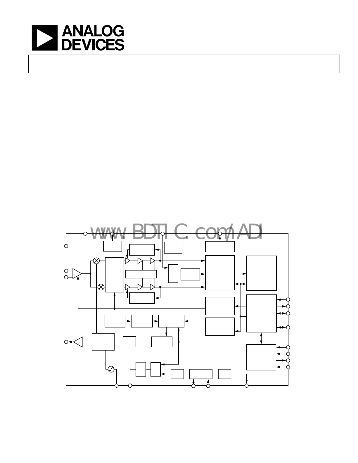
R
LNA
RFIN
RFINB
RFOUT
LNA
GAIN
LDO(1:4)
IF FILTER
FSK MOD
CONTROL
DIVIDERS/
MUXING
VCO
VCOIN CPOUT
FUNCTIONAL BLOCK DIAGRAM
DCINRSET CREG[1:4]
MODULATOR
N/N + 1DIV P
PFD
TEMP
SENSOR
MUX
Σ-Δ
DIV R
7-BIT ADC
Figure 1.
OSC1
OSC
OSC2
OFFSET
CORRECTION
RSSI
OFFSET
CORRECTION
GAUSSIAN
FILTER
CP
MUXOUT
TEST MUX
FSK/ASK
DEMODULATOR
AGC
CONTROL
AFC
CONTROL
CLK
DIV
SYNCHRONIZER
CONTROL
CLKOUT
ADF7020
DATA
Tx/Rx
SERIAL
PORT
CE
DATA CLK
DATA I/O
INT/LOCK
SLE
SDATA
SREAD
SCLK
05351-001
Rev. B
Information furnished by Analog Devices is believed to be accurate and reliable. However, no
responsibility is assumed by Anal og Devices for its use, nor for any infringements of patents or ot her
rights of third parties that may result from its use. Specifications subject to change without notice. No
license is granted by implication or otherwise under any patent or patent rights of Analog Devices.
Trademarks and registered trademarks are the property of their respective owners.
One Technology Way, P.O. Box 9106, Norwood, MA 02062-9106, U.S.A.
Tel: 781.329.4700 www.analog.com
Fax: 781.461.3113 ©2005–2007 Analog Devices, Inc. All rights reserved.

ADF7020
www.BDTIC.com/ADI
TABLE OF CONTENTS
Features.............................................................................................. 1
Applications....................................................................................... 1
Functional Block Diagram .............................................................. 1
Revision History ............................................................................... 3
General Description ......................................................................... 4
Specifications..................................................................................... 5
Timing Characteristics..................................................................... 8
Timing Diagrams.......................................................................... 8
Absolute Maximum Ratings.......................................................... 10
ESD Caution................................................................................ 10
Pin Configuration and Function Descriptions........................... 11
Typical Performance Characteristics ........................................... 13
Frequency Synthesizer ................................................................... 15
Reference Input........................................................................... 15
Choosing Channels for Best System Performance................. 17
Transmitter...................................................................................... 18
RF Output Stage.......................................................................... 18
Modulation Schemes.................................................................. 18
Receiver............................................................................................ 20
RF Front End............................................................................... 20
RSSI/AGC.................................................................................... 21
FSK Demodulators on the ADF7020....................................... 21
FSK Correlator/Demodulator................................................... 21
Linear FSK Demodulator .......................................................... 23
AFC .............................................................................................. 23
Automatic Sync Word Recognition .........................................24
Applications Information .............................................................. 25
LNA/PA Matching...................................................................... 25
Image Rejection Calibration ..................................................... 26
Transmit Protocol and Coding Considerations ..................... 27
Device Programming after Initial Power-Up ......................... 27
Interfacing to Microcontroller/DSP ........................................ 27
Power Consumption and battery lifetime calculations......... 28
Serial Interface ................................................................................ 31
Readback Format........................................................................ 31
Registers........................................................................................... 32
Register 0—N Register............................................................... 32
Register 1—Oscillator/Filter Register...................................... 33
Register 2—Transmit Modulation Register (ASK/OOK
Mode)........................................................................................... 34
Register 2—Transmit Modulation Register (FSK Mode) ..... 35
Register 2—Transmit Modulation Register (GFSK/GOOK
Mode)........................................................................................... 36
Register 3—Receiver Clock Register ....................................... 37
Register 4—Demodulator Setup Register ............................... 38
Register 5—Sync Byte Register................................................. 39
Register 6—Correlator/Demodulator Register ...................... 40
Register 7—Readback Setup Register...................................... 41
Register 8—Power-Down Test Register .................................. 42
Register 9—AGC Register......................................................... 43
Register 10—AGC 2 Register.................................................... 44
Register 11—AFC Register ....................................................... 44
Register 12—Test Register......................................................... 45
Register 13—Offset Removal and Signal Gain Register ....... 46
Outline Dimensions....................................................................... 47
Ordering Guide .......................................................................... 47
Rev. B | Page 2 of 48

ADF7020
www.BDTIC.com/ADI
REVISION HISTORY
8/07—Rev. A to Rev. B
Changes to Features..........................................................................1
Changes to General Description .....................................................4
Changes to Table 1 ............................................................................5
Changes to Table 2 ............................................................................8
Changes to Reference Input Section .............................................15
Changes to N Counter Section......................................................16
Changes to Choosing Channels for Best Performance Section 17
Changes to Table 5 ..........................................................................20
Changes to FSK Correlator Register Settings Section................22
Added Image Rejection Calibration Section ...............................26
Added Figure 41 ..............................................................................30
Changes to Readback Format Section..........................................31
Changes to Register 9—AGC Register Comments Section.......43
Added Register 12—Test Register Comments Section ..............45
4/06—Rev. 0 to Rev. A
Changes to Features..........................................................................1
Changes to Table 1 ............................................................................5
Changes to Figure 24 ......................................................................17
Changes to the Setting Up the ADF7020 for GFSK Section......19
Changes to Table 6 ..........................................................................21
Changes to Table 9 ..........................................................................23
Changes to External AFC Section.................................................23
Deleted Maximum AFC Range Section.......................................23
Added AFC Performance Section.................................................24
Changes to Internal Rx/Tx Switch Section..................................25
Changes to Figure 32 ......................................................................25
Changes to Transmit Protocol and Coding Considerations
S
ection ..............................................................................................26
Added Text Relating to Figure 37 .................................................27
Changes to Figure 41 ......................................................................31
Changes to Register 1—Oscillator/Filter Register
C
omments........................................................................................31
Changes to Figure 42 ......................................................................32
Changes to Register 2—Transmit Modulation Register
K Mode) Comments ................................................................. 33
(FS
Changes to Figure 44 ......................................................................34
Changes to Register 2—Transmit Modulation Register
(GFS
K/GOOK Mode) Comments................................................34
Changes to Register 4—Demodulator Setup Register
C
omments........................................................................................36
Changes to Figure 51 ......................................................................41
Changes to Figure 53 ......................................................................42
Changes to Ordering Guide...........................................................45
6/05—Revision 0: Initial Version
Rev. B | Page 3 of 48

ADF7020
www.BDTIC.com/ADI
GENERAL DESCRIPTION
The ADF7020 is a low power, highly integrated FSK/ASK/OOK
transceiver designed for operation in the license-free ISM bands
at 433 MHz, 868 MHz, and 915 MHz, as well as the proposed
Japanese RFID band at 950 MHz. A Gaussian data filter option
is available to allow either GFSK or G-ASK modulation, which
provides a more spectrally efficient modulation. In addition to
these modulation options, the ADF7020 can also be used to
perform both MSK and GMSK modulation, where MSK is a
special case of FSK with a modulation index of 0.5. The modulation index is calculated as twice the deviation divided by the
data rate. MSK is spectrally equivalent to O-QPSK modulation
with half-sinusoidal Tx baseband shaping, so the ADF7020 can
also support this modulation option by setting up the device in
MSK mode.
This device is suitable for circuit applications that meet the
uropean ETSI-300-220, the North American FCC (Part 15),
E
or the Chinese Short Range Device regulatory standards. A
complete transceiver can be built using a small number of
external discrete components, making the ADF7020 very
suitable for price-sensitive and area-sensitive applications.
The transmitter block on the ADF7020 contains a VCO and
l
ow noise fractional-N PLL with an output resolution of
<1 ppm. This frequency agile PLL allows the ADF7020 to be
used in frequency-hopping spread spectrum (FHSS) systems.
The VCO operates at twice the fundamental frequency to
reduce spurious emissions and frequency-pulling problems.
The transmitter output power is programmable in 0.3 dB steps
f
rom −16 dBm to +13 dBm. The transceiver RF frequency,
channel spacing, and modulation are programmable using a
simple 3-wire interface. The device operates with a power
supply range of 2.3 V to 3.6 V and can be powered down when
not in use.
A low IF architecture is used in the receiver (200 kHz),
mini
mizing power consumption and the external component
count and avoiding interference problems at low frequencies.
The ADF7020 supports a wide variety of programmable
features, including Rx linearity, sensitivity, and IF bandwidth,
allowing the user to trade off receiver sensitivity and selectivity
against current consumption, depending on the application.
The receiver also features a patent-pending automatic frequency
control (AFC) loop, allowing the PLL to track out the frequency
error in the incoming signal.
An on-chip ADC provides readback of an integrated temperat
ure sensor, an external analog input, the battery voltage, or the
RSSI signal, which provides savings on an ADC in some applications. The temperature sensor is accurate to ±10°C over the
full operating temperature range of −40°C to +85°C. This
accuracy can be improved by doing a 1-point calibration at
room temperature and storing the result in memory.
Rev. B | Page 4 of 48
ADF7020
www.BDTIC.com/ADI
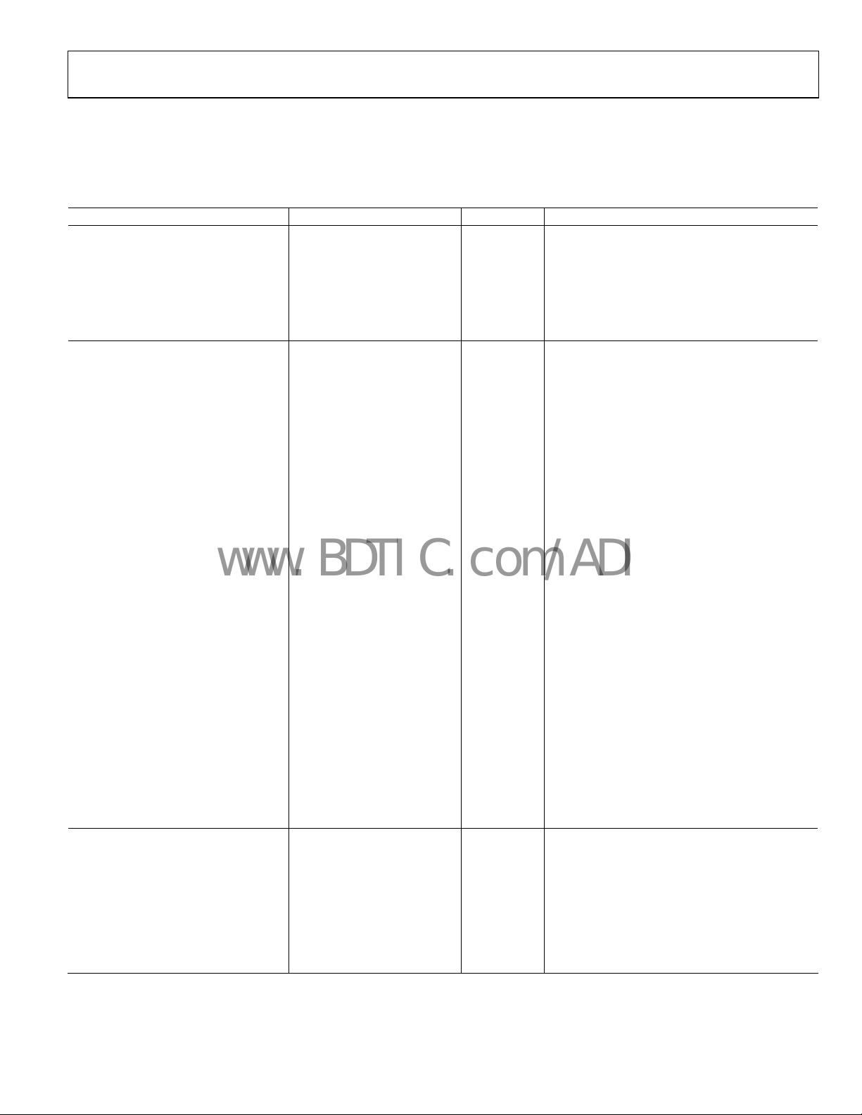
SPECIFICATIONS
VDD = 2.3 V to 3.6 V, GND = 0 V, TA = T
All measurements are performed using the EVAL-ADF7020DBZx using the PN9 data sequence, unless otherwise noted.
Table 1.
Parameter Min Typ Max Unit Test Conditions
RF CHARACTERISTICS
Frequency Ranges (Direct Output) 862 870 MHz VCO adjust = 0, VCO bias = 10
902 928 MHz VCO adjust = 3, VCO bias = 10
928 956 MHz VCO adjust = 3, VCO bias = 12, VDD = 2.7 V to 3.6 V
Frequency Ranges (Divide-by-2 Mode) 431 440 MHz VCO adjust = 0, VCO bias = 10
440 478 MHz VCO adjust = 3, VCO bias = 12
Phase Frequency Detector Frequency RF/256 24 MHz
TRANSMISSION PARAMETERS
Data Rate
FSK/GFSK 0.15 200 kbps
OOK/ASK 0.15 64
OOK/ASK 0.3 100 kbaud Using Manchester encoding
Frequency Shift Keying
GFSK/FSK Frequency Deviation
4.88 620 kHz PFD = 20 MHz
Deviation Frequency Resolution 100 Hz PFD = 3.625 MHz
Gaussian Filter BT 0.5
Amplitude Shift Keying
ASK Modulation Depth 30 dB
PA Off Feedthrough in OOK Mode −50 dBm
Transmit Power4 −20 +13 dBm VDD = 3.0 V, TA = 25°C
Transmit Power Variation vs.
Temperature
Transmit Power Variation vs. VDD ±1 dB From 2.3 V to 3.6 V at 915 MHz, TA = 25°C
Transmit Power Flatness ±1 dB From 902 MHz to 928 MHz, 3 V, TA = 25°C
Programmable Step Size
−20 dBm to +13 dBm 0.3125 dB
Integer Boundary −55 dBc 50 kHz loop BW
Reference −65 dBc
Harmonics
VCO Frequency Pulling, OOK Mode 30 kHz rms DR = 9.6 kbps
Optimum PA Load Impedance
48 + j54 Ω FRF = 868 MHz
54 + j94 Ω FRF = 433 MHz
RECEIVER PARAMETERS
FSK/GFSK Input Sensitivity At BER = 1E − 3, FRF = 915 MHz,
OOK Input Sensitivity At BER = 1E − 3, FRF = 915 MHz
Second Harmonic −27 dBc Unfiltered conductive
Third Harmonic −21 dBc
All Other Harmonics −35 dBc
Sensitivity at 1 kbps −119.2 dBm FDEV = 5 kHz, high sensitivity mode
Sensitivity at 9.6 kbps −112.8 dBm FDEV = 10 kHz, high sensitivity mode
Sensitivity at 200 kbps −100 dBm FDEV = 50 kHz, high sensitivity mode
Sensitivity at 1 kbps −116 dBm High sensitivity mode
Sensitivity at 9.6 kbps −106.5 dBm High sensitivity mode
2, 3
5
to T
MIN
1 110 kHz PFD = 3.625 MHz
±1 dB From −40°C to +85°C
39 + j61 Ω FRF = 915 MHz
, unless otherwise noted. Typical specifications are at VDD = 3 V, TA = 25°C.
MAX
1
kbps
LNA and PA matched separately
6
7
Rev. B | Page 5 of 48
ADF7020
www.BDTIC.com/ADI
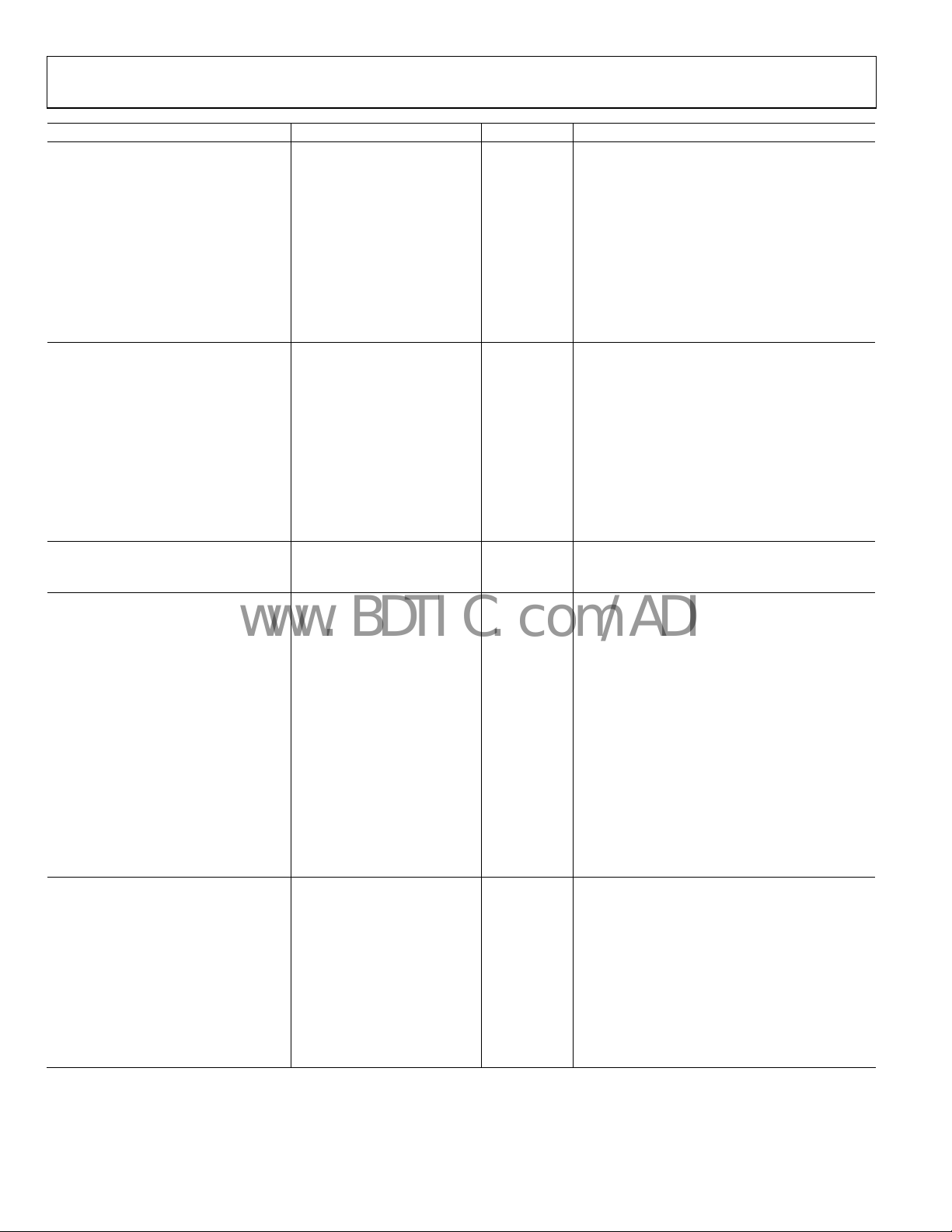
Parameter Min Typ Max Unit Test Conditions
LNA and Mixer, Input IP3
Enhanced Linearity Mode −3 dBm Pin = −20 dBm, 2 CW interferers
Low Current Mode −5 dBm FRF = 915 MHz, F1 = FRF + 3 MHz
High Sensitivity Mode −24 dBm F2 = FRF + 6 MHz, maximum gain
Rx Spurious Emissions
−47 dBm >1 GHz at antenna input
AFC
Pull-In Range at 868 MHz/915 MHz ±50 kHz IF_BW = 200 kHz
Pull-In Range at 433 MHz ±25 kHz IF_BW = 200 kHz
Response Time 48 Bits Modulation index = 0.875
Accuracy 1 kHz
CHANNEL FILTERING Desired signal 3 dB above the input sensitivity level,
Adjacent Channel Rejection
(Offset = ±1 × IF Filter BW Setting)
Second Adjacent Channel Rejection
(Offset = ±2 × IF Filter BW Setting)
Third Adjacent Channel Rejection
(Offset = ±3 × IF Filter BW Setting)
Image Channel Rejection
(Uncalibrated)
Image Channel Rejection (Calibrated) 50 dB Image at FRF = 400 kHz
CO-CHANNEL REJECTION −2 dB
Wideband Interference Rejection 70 dB Swept from 100 MHz to 2 GHz, measured as channel
BLOCKING Desired signal 3 dB above the input sensitivity level,
±1 MHz 60 dB
±5 MHz 68 dB
±10 MHz 65 dB
±10 MHz (High Linearity Mode) 72 dB
Saturation (Maximum Input Level) 12 dBm FSK mode, BER = 10−3
LNA Input Impedance 24 − j60 Ω FRF = 915 MHz, RFIN to GND
26 − j63 Ω FRF = 868 MHz
71 − j128 Ω FRF = 433 MHz
RSSI
Range at Input −110 to
Linearity ±2 dB
Absolute Accuracy ±3 dB
Response Time 150 μs
PHASE-LOCKED LOOP
VCO Gain 65 MHz/V 902 MHz to 928 MHz band,
130 MHz/V 860 MHz to 870 MHz band, VCO adjust = 0
65 MHz/V 433 MHz, VCO adjust = 0
Phase Noise (In-Band) −89 dBc/Hz PA = 0 dBm, VDD = 3.0 V, PFD = 10 MHz,
Phase Noise (Out-of-Band) −110 dBc/Hz 1 MHz offset
Residual FM 128 Hz From 200 Hz to 20 kHz, FRF = 868 MHz
PLL Settling 40 μs Measured for a 10 MHz frequency step to within
7
8
−57 dBm <1 GHz at antenna input
CW interferer power level increased until BER = 10
image channel excluded
27 dB IF filter BW settings = 100 kHz, 150 kHz, 200 kHz
50 dB IF filter BW settings = 100 kHz, 150 kHz, 200 kHz
55 dB IF filter BW settings = 100 kHz, 150 kHz, 200 kHz
30 dB Image at FRF = 400 kHz
rejection
CW interferer power level increased until BER = 10
−24
dBm
See the
VCO adjust = 0, VCO_BIAS_SETTING = 10
FRF = 915 MHz, VCO_BIAS_SETTING = 10
5 ppm accuracy, PFD = 20 MHz, LBW = 50 kHz
RSSI/AGC section
−3
−2
,
Rev. B | Page 6 of 48
ADF7020
www.BDTIC.com/ADI
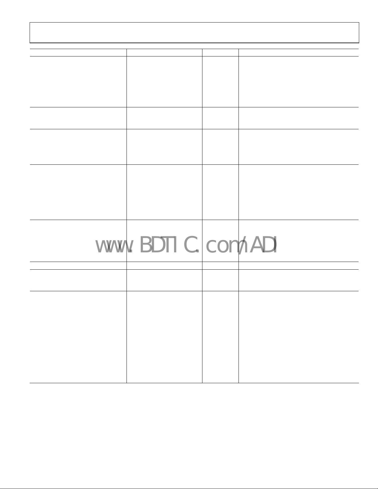
Parameter Min Typ Max Unit Test Conditions
REFERENCE INPUT
Crystal Reference 3.625 24 MHz
External Oscillator 3.625 24 MHz
Load Capacitance 33 pF See crystal manufacturer’s specification sheet
Crystal Start-Up Time 2.1 ms 11.0592 MHz crystal, using 33 pF load capacitors
1.0 ms Using 16 pF load capacitors
Input Level CMOS levels
ADC PARAMETERS
INL ±1 LSB From 2.3 V to 3.6 V, TA = 25°C
DNL ±1 LSB From 2.3 V to 3.6 V, TA = 25°C
TIMING INFORMATION
Chip Enabled to Regulator Ready 10 μs C
Chip Enabled to RSSI Ready 3.0 ms
Tx to Rx Turnaround Time 150 μs +
(5 × T
BIT
Time to synchronized data out, includes AGC settling;
)
LOGIC INPUTS
Input High Voltage, V
0.7 ×
INH
V
VDD
Input Low Voltage, V
0.2 ×
INL
V
VDD
Input Current, I
±1 μA
INH/IINL
Input Capacitance, CIN 10 pF
Control Clock Input 50 MHz
LOGIC OUTPUTS
Output High Voltage, VOH DVDD −
V IOH = 500 μA
0.4
Output Low Voltage, VOL 0.4 V IOL = 500 μA
CLK
Rise/Fall 5 ns
OUT
CLK
Load 10 pF
OUT
TEMPERATURE RANGE, TA −40 +85 °C
POWER SUPPLIES
Voltage Supply
VDD 2.3 3.6 V All VDD pins must be tied together
Transmit Current Consumption FRF = 915 MHz, VDD = 3.0 V,
−20 dBm 14.8 mA
−10 dBm 15.9 mA
0 dBm 19.1 mA
10 dBm 28.5 mA
10 dBm 26.8 mA PA matched separately with external antenna
Receive Current Consumption
Low Current Mode 19 mA
High Sensitivity Mode 21 mA
Power-Down Mode
Low Power Sleep Mode 0.1 1 μA
1
Higher data rates are achievable, depending on local regulations.
2
For the definition of frequency deviation, see the Register 2—Transmit Modulation Register (FSK Mode) section.
3
For the definition of GFSK frequency deviation, see the Register 2—Transmit Modulation Register (GFSK/GOOK Mode) section.
4
Measured as maximum unmodulated power. Output power varies with both supply and temperature.
5
For matching details, see the LNA/PA Matching section and the AN-764 Application Note.
6
Sensitivity for combined matching network case is typically 2 dB less than separate matching networks.
7
See Table 5 for a description of different receiver modes.
8
Follow the matching and layout guidelines to achieve the relevant FCC/ETSI specifications.
See the
Reference Input section
= 100 nF
REG
See
Table 11 for more details
see the
AGC Information and Timing section
PA is matched to 50 Ω
Combined PA and LNA matching network as on
EVAL-
ADF7020DBZx boards
VCO_BIAS_SETTING = 12
switch, VCO_BIAS_SETTING = 12
Rev. B | Page 7 of 48
ADF7020
www.BDTIC.com/ADI
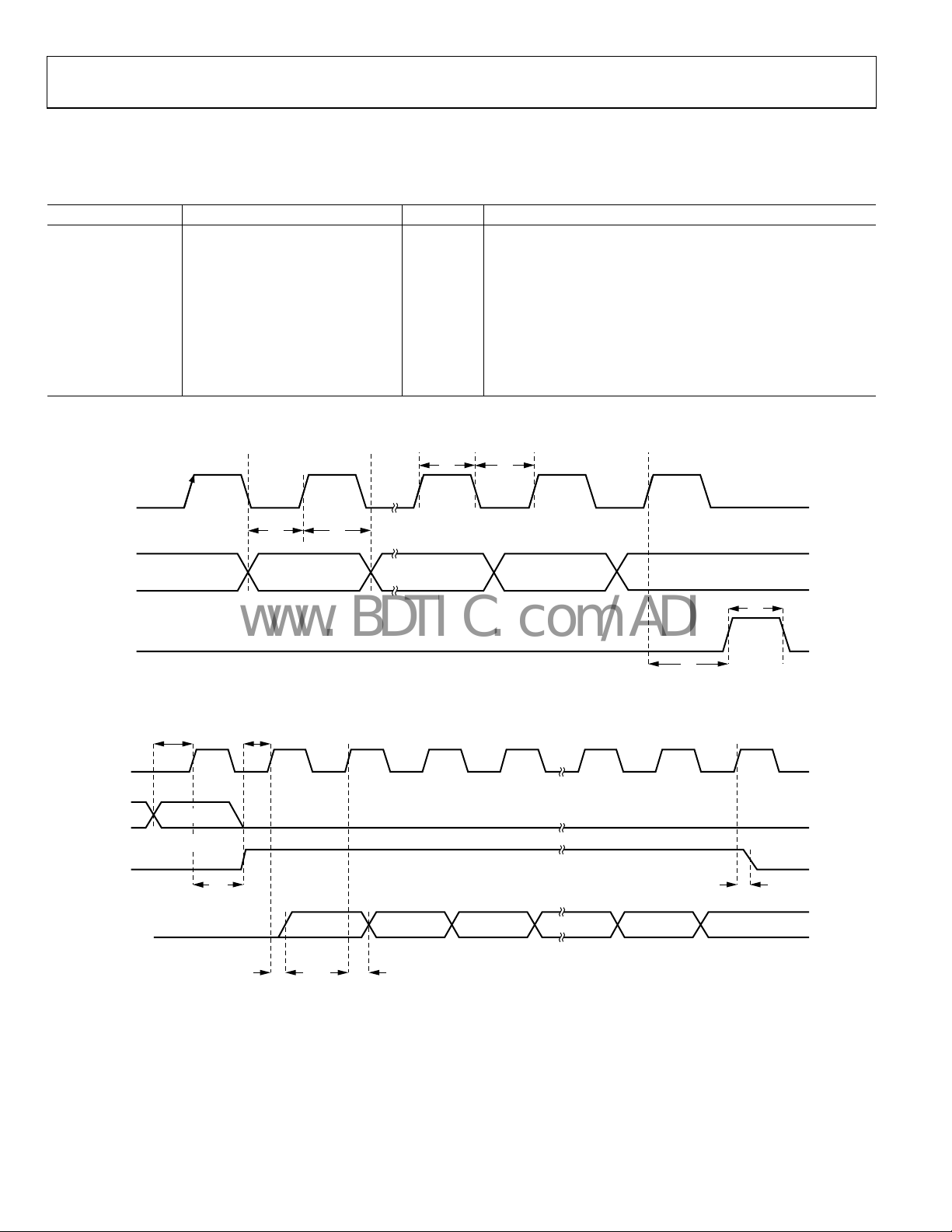
TIMING CHARACTERISTICS
VDD = 3 V ± 10%, VGND = 0 V, TA = 25°C, unless otherwise noted. Guaranteed by design, not production tested.
Table 2.
Parameter Limit at T
t
>10 ns SDATA to SCLK setup time
1
t2 >10 ns SDATA to SCLK hold time
t3 >25 ns SCLK high duration
t4 >25 ns SCLK low duration
t
>10 ns SCLK to SLE setup time
5
t
>20 ns SLE pulse width
6
t
<25 ns SCLK to SREAD data valid, readback
8
t
<25 ns SREAD hold time after SCLK, readback
9
t
>10 ns SCLK to SLE disable time, readback
10
TIMING DIAGRAMS
SCLK
MIN
to T
Unit Test Conditions/Comments
MAX
t
3
t
4
SDATA
SLE
t
1
DB31 (MSB) DB30 DB2
t
2
Figure 2. Serial Interface Timing Diagram
DB1
(CONTROL BIT C2)
DB0 (LSB)
(CONTROL BIT C1)
t
5
t
6
05351-002
SCLK
SDATA
SLE
SREAD
t
1
R7_DB0
(CONTROL BIT C1)
t
2
t
3
X RV16 RV15 RV2 RV1
t
t
8
9
Figure 3. Readback Timing Diagram
t
10
05351-003
Rev. B | Page 8 of 48
ADF7020
A
A
www.BDTIC.com/ADI
±1 × DATA RATE/32 1/DATA RAT E
RxCLK
RxDAT
DATA
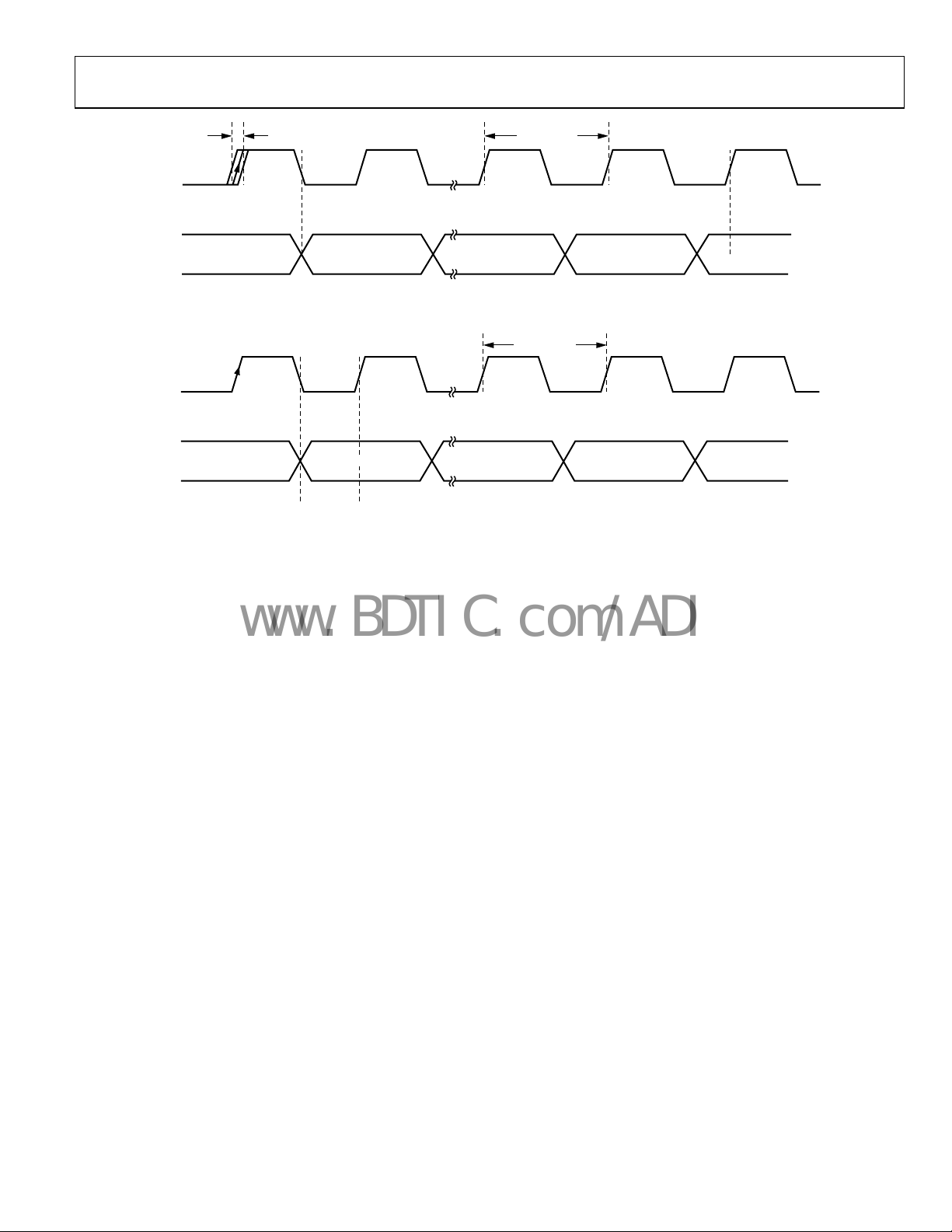
Figure 4. RxData/RxCLK Timing Diagram
05351-004
1/DATA RATE
TxCLK
TxDAT
NOTES
1. TxCLK ONLY AVAILABLE I N GFSK MODE.
SAMPLEFETCH
DATA
Figure 5. TxData/TxCLK Timing Diagram
5351-005
Rev. B | Page 9 of 48
ADF7020
www.BDTIC.com/ADI
ABSOLUTE MAXIMUM RATINGS
TA = 25°C, unless otherwise noted.
Table 3.
Parameter Rating
VDD to GND
Analog I/O Voltage to GND −0.3 V to AVDD + 0.3 V
Digital I/O Voltage to GND −0.3 V to DVDD + 0.3 V
Operating Temperature Range
Industrial (B Version) −40°C to +85°C
Storage Temperature Range −65°C to +125°C
Maximum Junction Temperature 150°C
MLF θJA Thermal Impedance 26°C/W
Reflow Soldering
Peak Temperature 260°C
Time at Peak Temperature 40 sec
1
GND = GND1 = RFGND = GND4 = VCO GND = 0 V.
1
−0.3 V to +5 V
Stresses above those listed under Absolute Maximum Ratings
may cause permanent damage to the device. This is a stress
rating only; functional operation of the device at these or any
other conditions above those indicated in the operational
section of this specification is not implied. Exposure to absolute
maximum rating conditions for extended periods may affect
device reliability.
This device is a high performance RF integrated circuit with an
D rating of <2 kV, and is ESD sensitive. Proper precautions
ES
should be taken for handling and assembly.
ESD CAUTION
Rev. B | Page 10 of 48
ADF7020
www.BDTIC.com/ADI
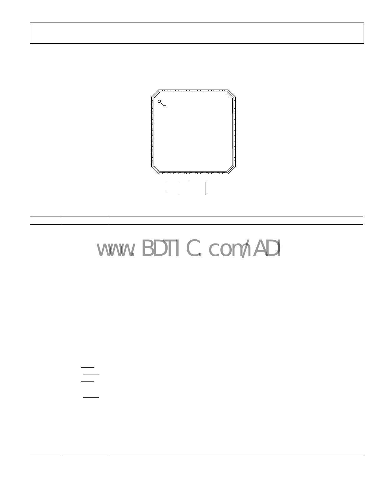
PIN CONFIGURATION AND FUNCTION DESCRIPTIONS
CVCO
GND1
GND
VCO GND
GND
VDD
CPOUT
CREG3
VDD3
OSC1
OSC2
MUXOUT
37
CLKOUT
36
DATA CLK
35
DATA I/O
34
33
INT/LOCK
VDD2
32
CREG2
31
ADCIN
30
GND2
29
SCLK
28
SREAD
27
SDATA
26
SLE
25
VCOIN
CREG1
VDD1
RFOUT
RFGND
RFIN
RFINB
R
LNA
VDD4
RSET
CREG4
GND4
4847464544434241403938
1
2
3
4
5
6
7
8
9
10
11
12
PIN 1
INDICATO R
ADF7020
TOP VIEW
(Not to Scale)
13141516171819
MIX_I
MIX_I
MIX_Q
MIX_Q
FILT_I
GND4
FILT_I
2021222324
GND4
FILT_Q
FILT_Q
TEST_A
CE
05351-006
Figure 6. Pin Configuration
Table 4. Pin Function Descriptions
Pin No. Mnemonic Description
1 VCOIN
The tuning voltage on this pin determines the output frequency of the voltage
-controlled oscillator (VCO).
The higher the tuning voltage, the higher the output frequency.
2 CREG1
3 VDD1
Regulator Voltage for PA Block. A 100 nF in parallel with a 5.1 pF capacitor should be placed between this
pin and gr
Voltage Supply for PA Block. Decoupling capacitors of 0.1 μF an
ound for regulator stability and noise rejection.
d 10 pF should be placed as close as
possible to this pin. All VDD pins should be tied together.
4 RFOUT
The modulated signal is available at this pin. Output po
wer levels are from −20 dBm to +13 dBm. The
output should be impedance matched to the desired load using suitable components. See the Transmitter
sec
tion.
5 RFGND Ground for Output Stage of Transmitter. All GND pins should be tied together.
6 RFIN
LNA Input for Receiver Section. Input matching is requi
red between the antenna and the differential LNA
input to ensure maximum power transfer. See the LNA/PA Matching section.
7 RFINB Complementary LNA Input. See the LNA/PA Matching section.
8 R
External bias resistor for LNA. Optimum resistor is 1.1 kΩ with 5% tolerance.
LNA
9 VDD4 Voltage Supply for LNA/MIXER Block. This pin should be decoupled to ground with a 10 nF capacitor.
10 RSET
External Resistor to Set Charge Pump Current and S
ome Internal Bias Currents. Use 3.6 kΩ with 5%
tolerance.
11 CREG4
Regulator Voltage for LNA/MIXER Block. A 100 nF capacitor should be placed bet
ween this pin and GND
for regulator stability and noise rejection.
12 GND4 Ground for LNA/MIXER Block.
13 to 18
MIX_I, MIX_I
MIX_Q, MIX_Q
FILT_I, FILT_I
Signal Chain Test Pins. These pins are high impedance under normal conditions and should be left
,
unconnected.
,
19, 22 GND4 Ground for LNA/MIXER Block.
20, 21, 23
FILT_Q, FILT_Q
TEST_A
24 CE
25 SLE
,
Signal Chain Test Pins. These pins are high impedance under normal conditions and should be left
unconnected.
Chip Enable. Bringing CE low puts the ADF7020 into complete power-down. Register values are lost when
w, and the part must be reprogrammed once CE is brought high.
CE is lo
Load Enable, CMOS Input. When LE goes high, the data stor
ed in the shift registers is loaded into one of
the fourteen latches. A latch is selected using the control bits.
26 SDATA
Serial Data Input. The serial da
ta is loaded MSB first with the two LSBs as the control bits. This pin is a high
impedance CMOS input.
Rev. B | Page 11 of 48
ADF7020
www.BDTIC.com/ADI
Pin No. Mnemonic Description
27 SREAD
28 SCLK
29 GND2 Ground for Digital Section.
30 ADCIN
31 CREG2
32 VDD2
33 INT/LOCK
34 DATA I/O Transmit Data Input/Received Data Output. This is a digital pin, and normal CMOS levels apply.
35 DATA CLK
36 CLKOUT
37 MUXOUT
38 OSC2
39 OSC1 The reference crystal should be connected between this pin and OSC2.
40 VDD3
41 CREG3
42 CPOUT
43 VDD Voltage Supply for VCO Tank Circuit. This pin should be decoupled to ground with a 0.01 μF capacitor.
44 to 47
48 CVCO A 22 nF capacitor should be placed between this pin and CREG1 to reduce VCO noise.
GND, GND1,
O GND
VC
Serial Data Output. This pin is used to feed readback da
SCLK input is used to clock each readback bit (AFC, ADC readback) from the SREAD pin.
Serial Clock Input. This serial clock is used to clock in the ser
the 24-bit shift register on the CLK rising edge. This pin is a digital CMOS input.
Analog-to-Digital Converter Input. The internal 7-bit ADC can be ac
to 1.9 V. Readback is made using the SREAD pin.
Regulator Voltage for Digital Block. A 100 nF in parallel with a 5.
this pin and ground for regulator stability and noise rejection.
Voltage Supply for Digital Block. A decoupling capacitor of 10 nF
this pin.
Bidirectional Pin. In output mode (in
found a match for the preamble sequence. In input mode (lock mode), the microcontroller can be used to
lock the demodulator threshold when a valid preamble has been detected. Once the threshold is locked,
NRZ data can be reliably received. In this mode, a demodulation lock can be asserted with minimum delay.
In receive mode, the pin outputs the synchronized data clock
center of the received data. In GFSK transmit mode, the pin outputs an accurate clock to latch the data
from the microcontroller into the transmit section at the exact required data rate. See the Gaussian
requency Shift Keying (GFSK) section.
F
A Divided-Down Version of the Crystal Reference with O
used to drive several other CMOS inputs, such as a microcontroller clock. The output has a 50:50 markspace ratio.
This pin provides the Lock_Detect signal, which is used t
frequency. Other signals include Regulator_Ready, which is an indicator of the status of the serial interface
regulator.
The reference crystal should be connected between this pin and OSC1. A TCXO reference can be used by
riving this pin with CMOS levels and disabling the crystal oscillator.
d
Voltage Supply for the Charge Pump and PLL Dividers. This pin should be dec
0.01 μF capacitor.
Regulator Voltage for Charge Pump and PLL Dividers. A 100 nF in parallel with a 5.1 pF capacitor should be
ed between this pin and ground for regulator stability and noise rejection.
plac
Charge Pump Output. This output generates current pul
integrated current changes the control voltage on the input to the VCO.
Grounds for VCO Block.
terrupt mode), the ADF7020 asserts the INT/ LOCK pin when it has
ta from the ADF7020 to the microcontroller. The
ial data to the registers. The data is latched into
cessed through this pin. Full scale is 0 V
1 pF capacitor should be placed between
should be placed as close as possible to
. The positive clock edge is matched to the
utput Driver. The digital clock output can be
o determine if the PLL is locked to the correct
oupled to ground with a
ses that are integrated in the loop filter. The
Rev. B | Page 12 of 48
ADF7020
–
g
V
Δ
www.BDTIC.com/ADI
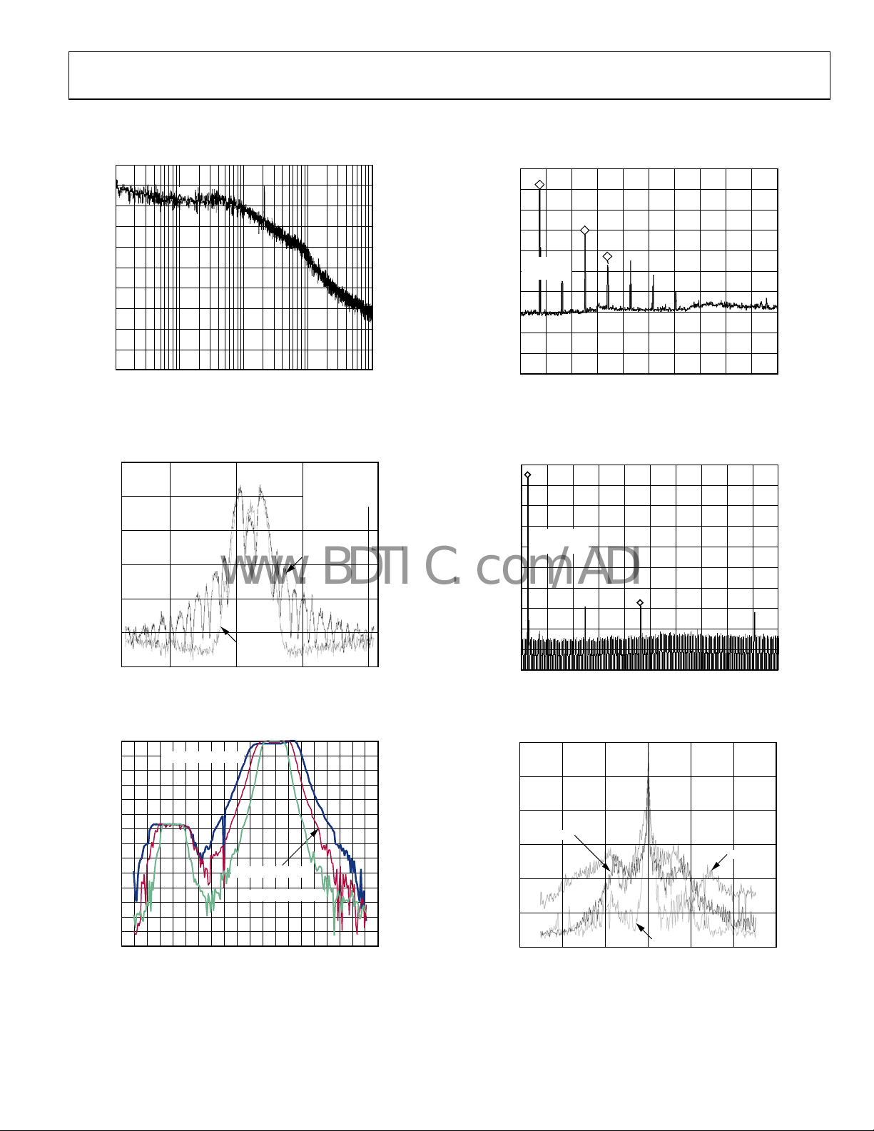
TYPICAL PERFORMANCE CHARACTERISTICS
CARRIER POWER
REF –70.00dBc/ Hz
10.00
dB/DIV
0.28dBm ATT EN 0.00dB MKR1
1
10.0000kHz
–87.80dBc/Hz
REF 10dBm
PEAK
lo
10dB/DI
1
REF LEVEL
10.00dBm
ATTEN 20dB
3
4
MKR4 3.482GHz
SWEEP 16.52ms (601pts)
1kHz FREQ UENCY OFFSET
10MHz
05351-007
Figure 7. Phase Noise Response at 868.3 MHz, VDD = 3.0 V, ICP = 1.5 mA
10
20
30
40
50
SIGNAL LE VEL (dBm)
60
70
Figure 8. Output Spectrum in
0
–5
–10
–15
–20
–25
–30
–35
–40
–45
–50
ATTENUATION LEVEL ( dB)
–55
–60
–65
–70
200kHz FILTER BW
GFSK
FREQUENCY (MHz)
150kHz FILT ER BW
IF FREQ (kHz)
Figure 9. IF Fil
FSK and GFSK Modulation
100kHz FILT ER BW
ter Response
PRBS PN9
DR = 7.1kbps
FDEV = 4.88kHz
RBW = 300kHz
FSK
913.38913.28 913.30 913. 32 913. 36
550–350 –250 –150 –50 50 150 250 350 450
05351-008
600–400 –300 –200 –100 0 100 200 300 400 500
05351-009
START 100MHz
RES BW 3MHz
Figure 10. Harmonic Response, RF
REF 15dBm ATTEN 30dB
1R
NORM
log
10dB/DIV
Δ
MARKER
1.834000000GHz
–62.57dB
LgAv
W1 S2
S3 FC
AA
£(f):
FTun
Swp
START 800MHz
#RES BW 30kHz
VBW 3MHz
OUT
1
VBW 30kHz
STOP 10.000GHz
SWEEP 16.52ms (601pts)
Matched to 50 Ω, No Filter
Mkr1 1.834GHz
–62.57dB
STOP 5. 000GHz
SWEEP 5. 627s (601pts)
05351-010
05351-011
Figure 11. Harmonic Response, Murata Dielectric Filter
10
0
–10
–20
–30
SIGNAL LEVEL (dBm)
–40
–50
Figure 12. Output Spectrum in ASK, OOK,
ASK
GOOK
FREQUENCY (MHz)
and GOOK Modes, DR = 10 kbps
OOK
900.80899.60 900.00899.80 900.20 900.40 900.60
05351-012
Rev. B | Page 13 of 48
ADF7020
R
R
R
–
www.BDTIC.com/ADI
20
15
10
5
0
–5
–10
PA OUTPUT POWE
–15
–20
–25
1 5 9 13172125293337414549535761
9µA
11µA
7µA
PA SETTING
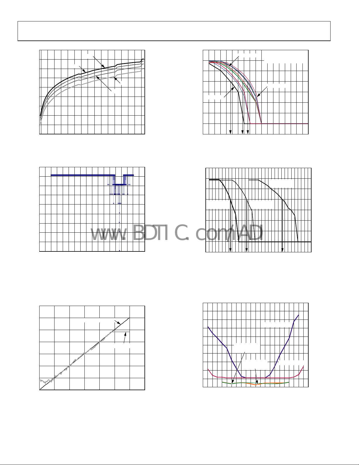
Figure 13. PA Output Power vs. Setting
5µA
05351-013
BE
0
–1
–2
–3
–4
3.6V, –40°C
–5
–6
–7
–8
–124
DATA RATE = 1kbp s FSK
IF BW = 100kHz
DEMOD BW = 0. 77kHz
2.4V, +85°C
–114
–115
–113
–116
–123
–122
3.0V, +25° C
–121
–120
–119
–118
RF INPUT LEVEL (dBm)
–117
Figure 16. BER vs. VDD and Temperature
–112
–111
–110
–109
–108
–107
–106
05351-016
80
70
60
50
40
30
20
10
LEVEL OF REJECTION (dB)
0
–10
200
250
300
350
400
450
500
550
600
650
700
750
800
850
900
FREQUENCY OF INTERFERER (MHz)
950
1000
1050
1100
Figure 14. Wideband Interference Rejection; Wanted Signal (880 MHz)
3 dB above Sensitivity Point
at
Interferer = FM Jammer (9.76 kbps, 10 kHz Deviation)
20
0
–20
–40
–60
RSSI LEVEL (dB)
–80
–100
–120
ACTUAL INPUT L EVEL
RSSI READBACK LEVEL
20–120 –100 –80 –60 –40 –20 0
RF INPUT (dB)
Figure 15. Digital RSSI Readback Linearity
0
–1
–2
–3
–4
BE
–5
–6
–7
–8
05351-014
1.002k
DATA RATE
–122
–121
–120
–119
–118
–117
–116
–115
–114
–113
–112
RF INPUT LEVEL (d Bm)
–111
–110
–109
9.760k
DATA RATE
Figure 17. BER vs. Data Rate (Comb
200.8k
DATA RATE
–108
–107
–106
–105
–104
–103
–102
–101
–100
ined Matching Network)
–99
–98
–97
–96
–90
–95
–94
–93
–92
–91
05351-017
Separate LNA and PA Matching Paths Typically
Improve Performance by 2 dB
60
–65
–70
–75
–80
–85
–90
–95
SENSITIVITY (dBm)
–100
–105
–110
–90
–110
05351-015
–100
CORRELATOR
AFC ON
CORRELATOR
–70
–50
–80
–30
–60
–40
FREQUENCY ERROR ( kHz)
AFC OFF
0
–10
–20
LINEAR AFC OFF
LINEAR AFC ON
10
30
50
20
40
60
70
90
80
110
100
05351-018
Figure 18. Sensitivity vs. Frequency Error with AFC On/Off
Rev. B | Page 14 of 48
ADF7020
P
www.BDTIC.com/ADI
FREQUENCY SYNTHESIZER
REFERENCE INPUT
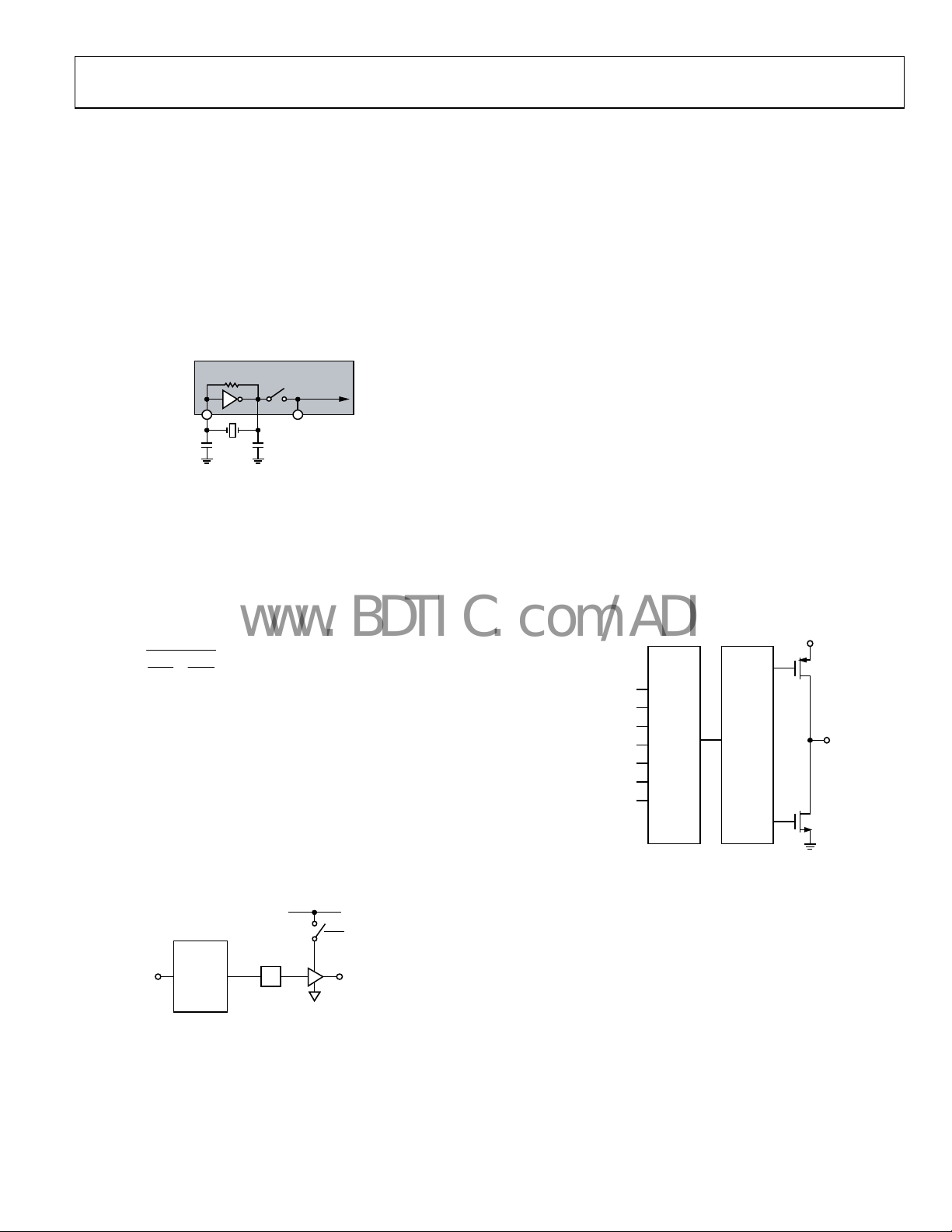
The on-board crystal oscillator circuitry (see Figure 19) can use
an inexpensive quartz crystal as the PLL reference. The oscillator circuit is enabled by setting R1_DB12 high. It is enabled by
default on power-up and is disabled by bringing CE low. Errors
in the crystal can be corrected using the automatic frequency
control (see the
f
ractional-N value (see the N Counter section). A single-ended
r
eference (TCXO, CXO) can also be used. The CMOS levels
should be applied to OSC2 with R1_DB12 set low.
Two parallel resonant capacitors are required for oscillation at
the correct frequency; their values are dependent on the crystal
specification. They should be chosen so that the series value of
capacitance added to the PCB track capacitance adds up to the
load capacitance of the crystal, usually 20 pF. PCB track
capacitance values might vary from 2 pF to 5 pF, depending on
board layout. Thus, CP1 and CP2 can be calculated using:
C +
L
Where possible, choose capacitors that have a low temperature
efficient to ensure stable frequency operation over all
co
conditions.
CLKOUT Divider and Buffer
The CLKOUT circuit takes the reference clock signal from the
oscillator section, shown in Figure 19, and supplies a divideddo
wn 50:50 mark-space signal to the CLKOUT pin. An even
divide from 2 to 30 is available. This divide number is set in
R1_DB[8:11]. On power-up, the CLKOUT defaults to
divide-by-8.
To disable CLKOUT, set the divide number to 0. The output
buffer can drive up to a 20 pF load with a 10% rise time at
4.8 MHz. Faster edges can result in some spurious feedthrough
to the output. A small series resistor (50 Ω) can be used to slow
the clock edges to reduce these spurs at f
AFC section) feature or by adjusting the
OSC1
Figure 19. Oscillator Circuit on the ADF7020
1
=
1
1
+
1
CP2C
DIVIDER
1 TO 15
Figure 20. CLKOUT Stage
OSC2
CP1CP2
C
PCB
DV
DD
÷2
CLK
.
05351-019
CLKOUT
ENABLE BIT
CLKOUTOSC1
05351-020
R Counter
The 3-bit R counter divides the reference input frequency by an
integer ranging from 1 to 7. The divided-down signal is
presented as the reference clock to the phase frequency detector
(PFD). The divide ratio is set in Register 1. Maximizing the
PFD frequency reduces the N value. Every doubling of the PFD
gives a 3 dB benefit in phase noise, as well as reducing
occurrences of spurious components. The R register defaults to
R = 1 on power-up.
PFD [Hz] = XTAL/R
MUXOUT and Lock Detect
The MUXOUT pin allows the user to access various digital
points in the ADF7020. The state of MUXOUT is controlled by
Bits R0_DB[29:31].
Regulator Ready
Regulator ready is the default setting on MUXOUT after the
transceiver has been powered up. The power-up time of the
regulator is typically 50 μs. Because the serial interface is
powered from the regulator, the regulator must be at its
nominal voltage before the ADF7020 can be programmed. The
status of the regulator can be monitored at MUXOUT. When
the regulator ready signal on MUXOUT is high, programming
of the ADF7020 can begin.
DV
DD
REGULATOR READY
DIGITAL LOCK DETECT
ANALOG LO CK DETECT
R COUNTER OUTPUT
N COUNTER OUTPUT
PLL TEST MODES
Σ-Δ TEST MODES
MUX CONTROL
Figure 21. MUXOUT Circuit
MUXOUT
DGND
Digital Lock Detect
Digital lock detect is active high. The lock detect circuit is
located at the PFD. When the phase error on five consecutive
cycles is less than 15 ns, lock detect is set high. Lock detect
remains high until 25 ns phase error is detected at the PFD.
Because no external components are needed for digital lock
detect, it is more widely used than analog lock detect.
Analog Lock Detect
This N-channel open-drain lock detect should be operated with
an external pull-up resistor of 10 kΩ nominal. When a lock has
been detected, this output is high with narrow low going pulses.
05351-021
Rev. B | Page 15 of 48
 Loading...